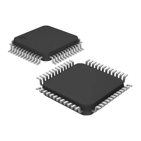
Motorola M68HC08 User manual

MOTOROLA.COM/SEMICONDUCTORS
M68HC08
Microcontrollers
DRM014/D
Rev. 0.0, 3/2003
USB and PS/2
Designer Reference
Multimedia Keyboard
Manual
Interface
Reference Design
Freescale Semiconductor, I
Freescale Semiconductor, Inc.
For More Information On This Product,
Go to: www.freescale.com
nc...

Freescale Semiconductor, I
Freescale Semiconductor, Inc.
For More Information On This Product,
Go to: www.freescale.com
nc...

DRM014 — Rev 0 Designer Reference Manual
MOTOROLA 3
USB and PS/2 Multimedia
Keyboard Interface
Reference Design
Designer Reference Manual — Rev
by: Derek Lau
Motorola Lt
Hong Kong
Freescale Semiconductor, I
Freescale Semiconductor, Inc.
For More Information On This Product,
Go to: www.freescale.com
nc...

Designer Reference Manual DRM014 — Rev 0
4MOTOROLA
Freescale Semiconductor, I
Freescale Semiconductor, Inc.
For More Information On This Product,
Go to: www.freescale.com
nc...

DRM014 — Rev 0 Designer Reference Manual
MOTOROLA Table of Contents 5
Designer Reference Manual — DRM 14
Table of Contents
Table of Contents
Section 1. USB and PS/2 Multimedia Keyboard Interface
1.1 Intro uction . . . . . . . . . . . . . . . . . . . . . . . . . . . . . . . . . . . . . . . . .7
1.2 Overview. . . . . . . . . . . . . . . . . . . . . . . . . . . . . . . . . . . . . . . . . . .7
1.3 44-pin QFP MC68HC908JB8 Features . . . . . . . . . . . . . . . . . . .8
1.4 Har ware Descriptions . . . . . . . . . . . . . . . . . . . . . . . . . . . . . . . .8
1.5 Firmware Description . . . . . . . . . . . . . . . . . . . . . . . . . . . . . . . .12
1.6 Firmware Files . . . . . . . . . . . . . . . . . . . . . . . . . . . . . . . . . . . . .29
1.7 Test Description . . . . . . . . . . . . . . . . . . . . . . . . . . . . . . . . . . . .30
1.8 Customization . . . . . . . . . . . . . . . . . . . . . . . . . . . . . . . . . . . . . .30
1.9 Extra Features . . . . . . . . . . . . . . . . . . . . . . . . . . . . . . . . . . . . .31
1.10 Further Information . . . . . . . . . . . . . . . . . . . . . . . . . . . . . . . . . .31
1.11 Schematics . . . . . . . . . . . . . . . . . . . . . . . . . . . . . . . . . . . . . . . .32
Section 2. Glossary
Freescale Semiconductor, I
Freescale Semiconductor, Inc.
For More Information On This Product,
Go to: www.freescale.com
nc...

Table of Contents
Designer Reference Manual DRM014 — Rev 0
6 Table of Contents MOTOROLA
Freescale Semiconductor, I
Freescale Semiconductor, Inc.
For More Information On This Product,
Go to: www.freescale.com
nc...

DRM014 — Rev 0 Designer Reference Manual
MOTOROLA USB an PS/2 Multime ia Keyboar Interface 7
Designer Reference Manual — DRM 14
Section 1. USB and PS/2 Multimedia Keyboard Interface
1.1 Introduction
This manual escribes a reference esign of a Universal Serial Bus an
PS/2 multime ia keyboar interface for Microsoft Win ows by using the
MC68HC908JB8.
For the full MC68HC908JB8 specification, please refer to the ata sheet,
Motorola or er number: MC68HC908JB8/D.
1.2 Overview
The Motorola MC68HC908JB8 is a member of the HC08 Family of
microcontrollers (MCUs). The features of the MC68HC908JB8 inclu e a
configure Universal Serial Bus (USB) or PS/2 interface, which makes
this MCU suite for personal computer Human Interface Devices (HID),
such as mice an keyboar s. The MC68HC908JB8 is available in
several packages to fit into various applications. A multime ia keyboar
with USB an PS/2 interface is emonstrate using the MC68HC908JB8
with a 44-pin QFP package. The main features of the keyboar inclu e:
• Fully USB specification 1.1 compliant
• USB or PS/2 interface auto etect
• Win ows 98, ME an 2000 compatible
• Power management keys (power, wake an sleep) support
• Multime ia key support
• In-circuit programming for firmware mo ification
Freescale Semiconductor, I
Freescale Semiconductor, Inc.
For More Information On This Product,
Go to: www.freescale.com
nc...

USB and PS/2 Multimedia Keyboard Interface
Designer Reference Manual DRM014 — Rev 0
8 USB an PS/2 Multime ia Keyboar Interface MOTOROLA
1.3 44-pin QFP MC68HC9 8JB8 Features
The 44-pin QFP MC68HC908JB8 is targete for USB an PS/2 interface
keyboar applications with minimum external components nee e .
Features inclu e:
• USB D+ an D– pins share with PS/2 ata an clock pins
• 27 out of 37 I/O pins with internal pull-up supports up to 8x19 key
matrix
• 10mA irect rive pins for the Num Lock, Caps Lock an Scroll
Lock LEDs
• Internal 1.5K pull-up for USB D– ata line
• Internal 5K pull-ups for PS/2 ata an clock pins
1.4 Hardware Descriptions
Figure 1-1. Block Diagram
Figure 1-2. USB and PS/2 Connections
MC68HC908JB8
8 x 18
Key Matrix
Scroll LED
Caps LED
Num LED
USB Plug
USB Plug USB to PS/2
Converter 12 4
6
5
3
PS/2 Plug
6-pin PS/2 Plug
1 – Data (USB D– pin)
2 – NC
3 – Ground (USB Ground)
4 – +5V (USB +5V)
5 – Clock (USB D+ pin)
6 – NC
Freescale Semiconductor, I
Freescale Semiconductor, Inc.
For More Information On This Product,
Go to: www.freescale.com
nc...

USB an PS/2 Multime ia Keyboar Interface
Har ware Descriptions
DRM014 — Rev 0 Designer Reference Manual
MOTOROLA USB an PS/2 Multime ia Keyboar Interface 9
Figure 1-1 shows the block iagram of the keyboar . The solution
inclu es the JB8, key button inputs an LED in icator outputs only. The
connections of the correspon ing USB an PS/2 signals are shown in
Figure 1-2. The USB to PS/2 converter stan ar connections are the
USB D– an D+ pins connecte to the PS/2 Data an Clock pins
respectively.
Figure 1-3 shows the printe circuit boar an Figure 1-16 shows the
schematic of the keyboar .
• J1 is use for USB connection
• J2 is use for PS/2 mouse connection (for future evelopment)
• J3 an J7 are use for in-circuit programming
• 8 rows x 18 columns key matrix is implemente
– 8 rows implemente in PTA[7:0]
– 18 columns implemente in PTB[7:0], PTC[7:0], PTE0 an
PTE2
• Keyboar LEDs
– Scroll Lock at PTD2
– Caps Lock at PTD3
– Num Lock at PTD4
Figure 1-4 shows the key matrix for the 107 stan ar keyboar with
power management keys (Power, Wake an Sleep). Figure 1-5 shows
the key matrix for multime ia keyboar with function key.
Freescale Semiconductor, I
Freescale Semiconductor, Inc.
For More Information On This Product,
Go to: www.freescale.com
nc...

USB and PS/2 Multimedia Keyboard Interface
Designer Reference Manual DRM014 — Rev 0
10 USB an PS/2 Multime ia Keyboar Interface MOTOROLA
Figure 1-3. Keyboard PCB
1.4.1 Key Matrix
Figure 1-4. 1 7-Key Matrix
ESC
Q
Z
5
F1
W
X
T
+
= F2
E
C
Bck
Spc
R
V
B
[ {
~
`
A
6] } TAB
2S
Y
“
‘
SPC
3D
H
<
,
N
F9
PTB PTB1 PTB2 PTB3 PTB4 PTB5 PTB6 PTB7 PTC PTC1 PTC2 PTC3 PTC4 PTC5 PTC6 PTC7 PTE
F
F3
F4
F5
F6
F7
F8
F1
F11
F12
INS DEL
Num
Lck
|
\
Prnt
Scr
Scrl
Lck Pause
App
89
UIO P
7
KL :
;
ENTM
>
.
Lctrl
J
4
9
*
4
56
7
23
+
ENT
.
/
1
Home Page
Up
Page
Down
End
RCTRL
PWR
Dwn
SLEEP
WAKE
RALT
LSFT
RSFT
LGUI
PTE2
Caps
Lck
RGUI
LALT
_
-
8
1
?
/
G
PTA
PTA1
PTA2
PTA3
PTA4
PTA5
PTA6
PTA7
Freescale Semiconductor, I
Freescale Semiconductor, Inc.
For More Information On This Product,
Go to: www.freescale.com
nc...

USB an PS/2 Multime ia Keyboar Interface
Har ware Descriptions
DRM014 — Rev 0 Designer Reference Manual
MOTOROLA USB an PS/2 Multime ia Keyboar Interface 11
Figure 1-5. Multimedia Key Matrix
ESC
QZ 5
F1
WX T +
=
F2
EC Q Bck
Spc
RV B [ {
~
`
1A 6 ] }
TAB
2S Y ‘ “
SPC
3D H$32
<
, NF9
PTA
PTA1
PTA2
PTA3
PTA4
PTA5
PTA6
PTA7
PTB PTB1 PTB2 PTB3 PTB4 PTB5 PTB6 PTB7 PTC PTC1 PTC2 PTC3PTC4 PTC5 PTC6 PTC7 PTE
F
F3
4
F4
F5
F6
F7
F8
F1
F11
F12
JPN3
INS
DEL
Num
Lck
|
\
Prnt
Scr
Scrl
Lck
Pause
$64
JPN1
$85
App
8
9
U
I
O
P
7
K
L
; :
ENT
M
>
.
Lctrl
J
8
9
*
4
5
6
7
2
3
+
ENT
.
/
1
Home
Page
Up
Page
Down
End
LCTRL
RCTRL
PWR
Dwn
SLEEP
WAKE
MK
MK6
MK1
MK4
RALT
JPN5
MK7 MK5
MK8
LSFT
RSFT
MK23
LANG
1
JPN4
MK2
LGUI
MK9
MK18
MK1
MK11
LANG
2
JPN2
PTE2
MK3
SLEEP
MK8
Caps
Lck
RGUI
Fn
LALT
_
-
Freescale Semiconductor, I
Freescale Semiconductor, Inc.
For More Information On This Product,
Go to: www.freescale.com
nc...

USB and PS/2 Multimedia Keyboard Interface
Designer Reference Manual DRM014 — Rev 0
12 USB an PS/2 Multime ia Keyboar Interface MOTOROLA
1.4.2 In-Circuit Programming
J3 an J7 contain all the signals for the MC68HC908JB8 to enter monitor
mo e for In-Circuit Programming. The ICP requires J3 an J7 to be
connecte with a cable to the ICP a aptor boar , which is plugge -into
the M68HC08 Serial Programmer (M68SPGRM08) (see Figure 1-6).
Running the MCUScribe software on the PC allows erase, programming
an verification of the firmware in the MC68HC908JB8. The
communication bau rate is etermine by the jumper setting of J3 of the
ICP a aptor boar . Connect pins 1 an 2 of J3 for 9600bps an pins 2
an 3 for 19200bps.
Figure 1-6. In-Circuit Programming Connection
1.5 Firmware Description
The firmware consists of three main parts:
• USB an PS/2 interface etection
• PS/2 main program an subroutines
• USB main program an subroutines
Freescale Semiconductor, I
Freescale Semiconductor, Inc.
For More Information On This Product,
Go to: www.freescale.com
nc...

USB an PS/2 Multime ia Keyboar Interface
Firmware Description
DRM014 — Rev 0 Designer Reference Manual
MOTOROLA USB an PS/2 Multime ia Keyboar Interface 13
Figure 1-7. USB and PS/2 Detection
DELAY 350ms (POWER ON DELAY)
INITIALIZATION
ENABLE USB D– PULLUP
D+ HIGH FOR 1ms ?
OVER 10 SECONDS ?
USB RESET?
D+ HIGH FOR 1ms ?
NO
NO
NO
YES
SETUP DETECTED ?
NO
OVER 10 SECONDS ?
NO
NO
PS/2
USB
PS/2
USB
USB
YES
YES
YES
YES
YES
Freescale Semiconductor, I
Freescale Semiconductor, Inc.
For More Information On This Product,
Go to: www.freescale.com
nc...

USB and PS/2 Multimedia Keyboard Interface
Designer Reference Manual DRM014 — Rev 0
14 USB an PS/2 Multime ia Keyboar Interface MOTOROLA
1.5.1 USB and PS/2 Detection
PTE3 an PTE4 can be configure as USB D+ an D– pins or as
open- rain I/O pins for PS/2 ata an clock lines. Figure 1-7 shows the
algorithm for istinguishing between a USB an a PS/2 interface.
After power on, the interface protocol is un etermine an can be either
a USB or a PS/2 interface. The firmware first initializes the registers an
the I/O ports. It then performs a 350ms software elay to meet the PS/2
power on elay requirement. The USB engine an the internal USB
pullup resistor are enable . PTE3 an PTE4 are configure as USB D+
an D– pins with a 1.5K internal pullup at D– pin.
For a low spee USB interface, D+ pin will not be continuously high for
more than 4µs because of the bit stuffing mechanism. The PS/2
interface is etermine by 1ms continuously high at D+ pin while the
USB interface is etermine by receiving a SETUP token.
After the interface mo e is etecte . the firmware enters either the PS/2
main routine or the USB main routine.
1.5.2 PS/2 Main Routine
In PS/2 mo e, PTE3 an PTE4 are configure as open- rain I/O pins
with 5K internal pullup resistors enable . Figure 1-8 shows the PS/2
main routine. The main functions of the PS/2 routines are:
• Receive comman s from host
• Respon to receive comman s
• Scan key matrix
• Sen make co e to host if key presse
• Sen break co e to host if key release
Freescale Semiconductor, I
Freescale Semiconductor, Inc.
For More Information On This Product,
Go to: www.freescale.com
nc...

USB an PS/2 Multime ia Keyboar Interface
Firmware Description
DRM014 — Rev 0 Designer Reference Manual
MOTOROLA USB an PS/2 Multime ia Keyboar Interface 15
Figure 1-8. PS/2 Main Routine
SEND SELF TEST
FAIL CODE ($FC)
SEND SELF TEST PASS
CODE ($AA)
PS/2 INITIALIZATION
SELF
40ms TIMER TICK ?
YES
KEYS PRESSED
TEST PASS ?
SCAN KEY MATRIX
YES
SEND MAKE CODES
NO
YES
STOP
OR RELEASED
FOR KEYS PRESSED
SEND BREAK CODES
FOR KEYS RELEASED
ACK AND
VALID COMMAND
FROM HOST ?
HANDLE COMMAND
NO
YES
GHOST KEY ?
NO
NO
YES
SEND SELF TEST PASS
CODE ($AA)
SEND SELF TEST
FAIL CODE ($FC)
Freescale Semiconductor, I
Freescale Semiconductor, Inc.
For More Information On This Product,
Go to: www.freescale.com
nc...

USB and PS/2 Multimedia Keyboard Interface
Designer Reference Manual DRM014 — Rev 0
16 USB an PS/2 Multime ia Keyboar Interface MOTOROLA
1.5.3 PS/2 Protocol
The PS/2 is a bi irectional serial interface using two signals: Clock an
Data. The ata consists of 11 bits inclu ing 1 start bit, 8 ata bits, 1 o
parity bit, an 1 stop bit. PS/2 evice generates the clock signal with a
typical cycle of 80µs in both host-to- evice or evice-to-host
communications.
Table 1-1 shows the setting of the registers for controlling the PTE3
(Clock) an the PTE4 (Data) pins. Instea of setting DDR3/DDR4 as
high to output a high signal, we set DDR3/DDR4 as an input with internal
pullup to perform the same function. In the PS/2 routines, the values of
PTE3 an PTE4 are cleare to zero an the values of PTE3P an
PTE4P are set to one. Set DDR3 or DDR4 to one to force it as output
low, or clear DDR3 or DDR4 to zero to make it high impe ance an
pulle high by the 5K internal resistor.
1.5.4 Host to Device Communications
Data sent from host to evice is rea while the clock line is high. In an
i le state, both the Clock an the Data lines are pulle high. The host
starts sen ing ata by pulling the Clock line low for a minimum of 100ms.
Figure 1-9 shows the signal iagram. Communications steps are shown
as below:
1. Host waits until no auxiliary evice transmission is in progress.
Table 1-1. Clock and Data Line Control
Register Bits Port Pins
Register POCR PTE DDRE IOCR POCR PTE DDRE PTE4
(Data) PTE3
(Clock)
Bit PTE4P PTE4 DDRE4 PTE4IE PTE3P PTE3 DDRE3 PTE4
(Data) PTE3
(Clock)
PTE4
Interrupt
Enabled
——— 1 ———
Input
High —
Release
Data/Clock
High
1—0—1—0
Input
High
Input
High
Drive
Data/Clock
Low
—0 1——0 1
Output
Low
Output
Low
Freescale Semiconductor, I
Freescale Semiconductor, Inc.
For More Information On This Product,
Go to: www.freescale.com
nc...

USB an PS/2 Multime ia Keyboar Interface
Firmware Description
DRM014 — Rev 0 Designer Reference Manual
MOTOROLA USB an PS/2 Multime ia Keyboar Interface 17
2. Host pulls the Clock line low.
3. Host pulls the Data line low as the start bit.
4. Host releases the Clock line.
5. Device pulls Clock line low.
6. Host sen s out ata.
7. Device releases the Clock line high an rea Data.
8. Device rea s the Clock line an aborts communication if the Clock
line is low.
9. Repeat steps 5 to 7 for Data 1 to Data 7 an the parity bit.
10. Device pulls the Clock line low.
11. Host releases the Data line.
12. Device releases the Clock line high.
13. Device rea s the Data line high for stop signal an sen s error if
the Data line is low.
14. Device pull the Data an the Clock lines low.
15. Device release the Clock an the Data lines.
Figure 1-9. Host to Device Communication
KBD_IN is the IRQ1 interrupt routine for receiving ata from host. The
interrupt is configure to execute when a falling e ge at the PTE4 (Data)
pin is etecte .
CLOCK
DATA
START DATA0 DATA1 DATA2 DATA3 DATA4 DATA5 DATA6 DATA7 PARITYSTOP ACK
2
36
11,13
12STEP 1 4 7,8
9
10
14
15
5
Freescale Semiconductor, I
Freescale Semiconductor, Inc.
For More Information On This Product,
Go to: www.freescale.com
nc...

USB and PS/2 Multimedia Keyboard Interface
Designer Reference Manual DRM014 — Rev 0
18 USB an PS/2 Multime ia Keyboar Interface MOTOROLA
1.5.5 Device to Host Communications
Data sent from evice to host is rea at the falling e ge of the clock. The
evice checks whether the host is rea y by etecting the clock high
before transmitting ata. Figure 1-10 shows the signal iagram.
Communications steps are shown as below:
1. Device waits for the Clock line high for a minimum of 50ms.
2. Abort if the Data line is low.
3. Device sen s out ata.
4. Device pulls the Clock line low.
5. Device releases the Clock line high.
6. Device rea s the Clock line an aborts communication if the Clock
line is low.
7. Repeat steps 4 to 6 for Data 0 to Data 7, the parity bit an the stop
bit.
8. Device releases the Clock line high.
Figure 1-1 . Device to Host Communication
KBD_OUT is the routine for transmitting ata to the host. The ata to be
transmitte is put into V_TxByte before calling this routine.
1.5.6 PS/2 Keyboard Command
Both the host an the keyboar may sen comman s to each other. The
keyboar transmits an acknowle ge ($FA) after receiving a vali
CLOCK
DATA
START DATA0 DATA1 DATA2 DATA3 DATA4 DATA5 DATA6 DATA7 PARITY STOP
3
STEP 1,2
4
5,6
8
7
Freescale Semiconductor, I
Freescale Semiconductor, Inc.
For More Information On This Product,
Go to: www.freescale.com
nc...

USB an PS/2 Multime ia Keyboar Interface
Firmware Description
DRM014 — Rev 0 Designer Reference Manual
MOTOROLA USB an PS/2 Multime ia Keyboar Interface 19
comman . When the keyboar receives an invali comman , it returns
a resent comman ($FA).
1.5.7 Host to Keyboard Commands
1.5.8 Keyboard to Host Commands
Table 1-2. Host to Keyboard Commands
Code Description Implemented
$ED Set status in icators YES
$EE Echo YES
$F0 Set alternate Scan Co e NO
$F2 Get keyboar ID YES
$F3 Set typematic repeat rate YES
$F4 Enable Scan YES
$F5 Disable Scan YES
$F6 Set efault values YES
$F7 Set all keys typematic NO
$F8 Set all keys make/break NO
$F9 Set all keys make NO
$FA Set key type typematic/make/break NO
$FB Set key type typematic NO
$FC Set key type make/break NO
$FD Set key type make NO
$FE Resent the last comman YES
$FF Reset YES
Table 1-3. Keyboard to Host Commands
Code Description Implemented
$00 Keyboar etection or overrun error YES
$AA Basic assurance test passe YES
$EE Echo YES
$FA Acknowle ge YES
$FE Resen YES
Freescale Semiconductor, I
Freescale Semiconductor, Inc.
For More Information On This Product,
Go to: www.freescale.com
nc...

USB and PS/2 Multimedia Keyboard Interface
Designer Reference Manual DRM014 — Rev 0
20 USB an PS/2 Multime ia Keyboar Interface MOTOROLA
1.5.9 PS/2 Scan Codes
There are three sets of scan co es (co e 1, 2, an 3). Most PCs support
scan co e set 2, hence this is the only scan co e the firmware supports.
Make co e or break co e is sent when any key is presse or release .
While a key is presse , its make co e is sent out repeate ly an the rate
epen s on the typematic repeat value.
In a ition to the IBM stan ar , Microsoft has publishe stan ar s for
the Win ows keys, Power Management keys (sleep, wake, an power),
an the Au io Control keys.
Table 1-4. Scan codes supported by Windows 98, ME, and 2
Description Make Code Break Code
Left Win ows $E0, $1F $E0, $F0, $1F
Right Win ows $E0, $27 $E0, $F0, $27
Applications $E0, $2F $E0, $F0, $2F
Power $E0, $37 $E0, $F0, $37
Sleep $E0, $3F $E0, $F0, $3F
Wake $E0, $5E $E0, $F0, $5E
Table 1-5. Scan codes supported by Windows ME and 2
Description Make Code Break Code
Scan next track $E0, $4D $E0, $F0, $4D
Scan previous track $E0, $15 $E0, $F0, $15
Stop $E0, $3B $E0, $F0, $3B
Play/Pause $E0, $34 $E0, $F0, $34
Mute $E0, $23 $E0, $F0, $23
Volume increase $E0, $32 $E0, $F0, $32
Volume ecrease $E0, $21 $E0, $F0, $21
AL Email Rea er $E0, $48 $E0, $F0, $48
AC search $E0, $10 $E0, $F0, $10
AC Home $E0, $3A $E0, $F0, $3A
AC Forwar $E0, $30 $E0, $F0, $30
AC Stop $E0, $28 $E0, $F0, $28
AC Reflesh $E0, $20 $E0, $F0, $20
AC Bookmarks $E0, $18 $E0, $F0, $18
Freescale Semiconductor, I
Freescale Semiconductor, Inc.
For More Information On This Product,
Go to: www.freescale.com
nc...
Other manuals for M68HC08
3
Table of contents
Other Motorola Microcontroller manuals
Motorola
Motorola MPC533 User manual
Motorola
Motorola AT Commands G24-L Manual

Motorola
Motorola DSP56824ADM User manual
Motorola
Motorola MPC860 PowerQUICC User manual

Motorola
Motorola MCU M68MPB916R3 User manual

Motorola
Motorola F3030A Instruction Manual

Motorola
Motorola MC9S12DT256 User manual

Motorola
Motorola M68MPB334 User manual
Motorola
Motorola MC68HC05T16 Instruction manual

Motorola
Motorola M68HC08 User manual