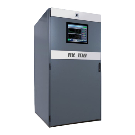
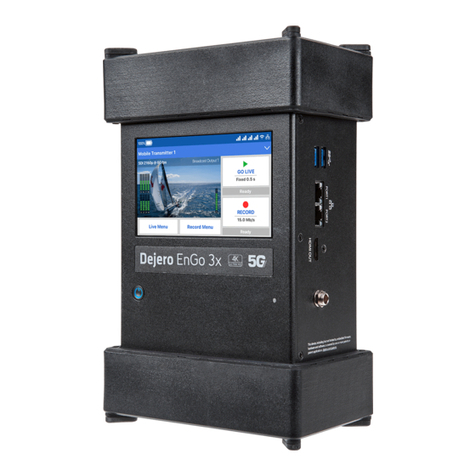
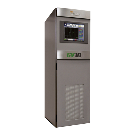
Nautel NX300 User manual

NX300 Transmitter
Operations and Maintenance
Manual
Document:NHB-NX300-OPS-3.0
Issue: 3.0 2012-11-01
Status: Standard


Nautel Limited
10089 Peggy’s Cove Road
Hackett’s Cove, NS Canada B3Z 3J4
Phone: +1.902.823.3900 or
Toll Free: +1.877.6NAUTEL (6628835) (Canada & USA only)
Fax: +1.902.823.3183
Nautel Inc.
201 Target Industrial Circle
Bangor, Maine USA 04401
Phone: +1.207.947.8200
Fax: +1.207.947.3693
Customer Service (24 hour support)
+1.877.628.8353 (Canada & USA only)
+1.902.823.5100 (International)
Email: [email protected]
Web: www.nautel.com
The comparisons and other information provided in this document
have been prepared in good faith based on publicly available
information. The reader is encouraged to consult the respective
manufacturer's most recent published data for verification.
© Copyright 2012 NAUTEL. All rights reserved.


NX300 Operations and Maintenance Manual Table of contents
Page v
Contents
Release control record vii
Description 1-1
Ac-dc power stage 1-1
Exciter stage 1-2
Control/monitor stage 1-4
RF power stage 1-5
RF output network 1-5
Operating the transmitter 2-1
Using the AUI 2-2
Home page - describing the first page 2-17
Menu page - describing transmitter operations 2-18
Viewing Transmitter Log 2-20
Instrument Panels - viewing displays 2-27
Meters page - viewing real-time meters 2-42
Presets - editing operational settings 2-48
Preset Scheduler 2-61
Status - viewing transmitter status 2-64
User Accounts 2-66
User Settings 2-71
System Settings page 2-89
Precorrection Settings page 2-97
Changeover page - changing exciter transfer settings 2-106
Factory Settings 2-107
Remote I/O page 2-116
Playlist Manager 2-121
Using the key-controlled access system 2-126

NX300 Operations and Maintenance Manual Table of contents
Page vi Issue 3.0 2012-11-01
Routine maintenance 3-1
Scheduled maintenance 3-1
Replacing a damaged air filter 3-2
Performing on-air checks 3-3
Replacing the control/interface PWB battery 3-4
Inspecting lightning protection systems 3-5
Non-standard maintenance 4-1
Upgrading software 4-1
List of terms 5-1

NX300 Operations and Maintenance Manual
Issue 3.0 2012-11-01 Page vii
Release control record
Issue Date Reason
3.0 2012-11-01 Release 3 of product (NARA54B)
Software Release NX4.0

NX300 Operations and Maintenance Manual
Page viii Issue 3.0 2012-11-01

NX300 Operations and Maintenance Manual Description
Issue 3.0 2012-11-01 Page 1-1
Section 1: Description
Refer to the functional block diagram: Figure 1.6 on page 1-11.
This section provides a high-level description of the transmitter’s key sections. The transmitter
circuitry is subdivided into five basic stages.
•Ac-dc power stage
•Exciter stage - see page 1-2
•Control/monitor stage - see page 1-4
•RF power stage - see page 1-5
•RF output network - see page 1-5 (includes combiner and filter)
NX300 electrical schematics
Some descriptions in this section refer to electrical schematics (SD-#s) . These are located at the end
of the NX300 Troubleshooting Manual.
Redundancy
The NX300 features redundancy in all key systems:
• RF power modules
• Exciters
• Cooling fans
Ac-dc power stage
See electrical schematic SD-1. The ac/dc power supply stage contains the input power transformer
that receives the main ac input to the transmitter. It also contains the transmitter’s low voltage power
supplies and rack interface PWB. The ac/dc power supply stage also include a three-phase SCR
rectifier assembly, Hall Effect current sensor, and B+ distribution assemblies. With the exception of
the power transformer, which has its own cabinet, each cabinet in the transmitter system contains its
own ac/dc power stage components.

NX300 Operations and Maintenance Manual Description
Page 1-2 Issue 3.0 2012-11-01
The secondary of the power transformer is applied to the SCR rectifier assembly to create the
transmitter’s B+ voltage. The output of the rectifier assembly is fed through the Hall Effect current
sensor, which supplies a dc current signal to the rack interface PWB. The rectifier assembly output is
applied to the B+ distribution assemblies, which then provide the B+ voltage to the RF power
modules, and a B+ sample to the rack interface PWB.
One phase of the power transformer’s secondary is also used to provide a source for the low voltage
dc power supplies and an ac sample for the rack interface PWB. The low voltage power supply
outputs (+48 V, +15 V and +12 V) are distributed throughout the transmitter via the rack interface
PWB.
Ac power transformer
The NX300’s power transformer can be set to use a range of input voltages. See Section 4,
“Connecting transformer taps/load wiring” on page 4-1 in the NX300 Installation Manual.
Exciter stage
See electrical schematic SD-2 and Figure 1.1 on page 1-3. The exciter stage consists of digital AM
exciter PWBs A (A11A2) and B (A11A3), RF drive distribution PWB (A16), and PDM distribution
PWB (A17). The dual digital AM exciter PWBs provide two independent exciter sections (A and B),
which can be selected automatically or by local or remote control. The control/interface PWB acts as
an interface point for audio inputs and RF drive and PDM outputs.
Digital AM exciter PWBs
Digital AM exciter PWBs A (A11A2) and B (A11A3) accept audio or IBOC inputs from an
integrated DRM exciter or Exgine card and generate fully digital RF drive carrier frequency sources
and interphase PDM drive signals for the power amplifiers and modulators in the RF power modules.
Audio input can be applied as as analog (balanced or AES-EBU) or digital (I/Q in AES/EBU or
CMOS format). All audio inputs are digitized, as necessary, and sample rate converted. A DSP
provides initial data conditioning, including the initial filtering and interpolation of incoming audio or
digital radio data.
An FPGA generates the digital PDM signals and synthesizes the carrier frequency RF drive signal. It
also performs digital up-conversion, reverse path demodulation and downconversion and B+ voltage
compensation.

NX300 Operations and Maintenance Manual Description
Issue 3.0 2012-11-01 Page 1-3
Figure 1.1: Exciter Stage
The digital PDM component consists of nine phased PDM signals, each separated by 40 electrical
degrees. These PDM drive signals determine the transmitter output power level as well as the output
modulation level. Three of these phases, each separated by 120 electrical degrees (e.g., 1, 4 and 7), are
applied to a given RF power module. To achieve optimal harmonic cancellation, three different
phases (e.g., 2, 5 and 8) are applied to the adjacent module, and three other phases (e.g., 3, 6 and 9) are
applied to the next module.
Samples of the RF output voltage, RF output current and RF power module temperature are
monitored. If a parameter exceeds an acceptable limit, the active exciter attempts to compensate by
decreasing its output power to restore the parameter to an acceptable level.
A sample of the B+ supply voltage is monitored. A B+ compensation circuit attempts to regulate the
regulated B+ supply in order to hold the transmitter output power constant and mimimize distortion.
An inhibit PDM input is applied from the control/display PWB to inhibit the PDM drive during
certain alarm/fault conditions.
RF drive distribution
The control/interface PWB (A11A1) accepts the RF drive (+ and -) signals from the digital AM
exciter PWBs (A and B) and splits the active exciter’s RF drive signal for application to each cabinet’s
RF drive distribution PWB (A16). The RF drive distribution PWB splits the signal from the control/
interface PWB and buffers the individual outputs that are provided to the RF power stage.
Digital AM
Exciter A
+15 V dc
-15 V dc
+5 V dc
Audio/
IBOC/
DRM
Inputs
Digital AM
Exciter B
Control/Interface
Audio/
IBOC
Inputs
Control/Interface
RF Drive (A)
RF Drive (B)
PDM (A) 1-9
PDM (B) 1-9
RF Drive 1
RF Drive 2
PDM 1-9
RF Drive
Distribution
PDM
Distribution
To RF Power Modules

NX300 Operations and Maintenance Manual Description
Page 1-4 Issue 3.0 2012-11-01
PDM distribution
The control/interface PWB (A11A1) accepts the PDM (1 through 9) signals from the digital AM
exciter PWBs (A and B) and splits the active exciter PDM signals for application to each cabinet’s
PDM distribution PWB (A17). The PDM distribution PWB accepts each signal from the control/
interface PWB and splits it into two (+ and -) opposite logic outputs that are provided to the RF
power stage.
Control/monitor stage
See electrical schematic SD-3 and Figure 1.2 on page 1-4.
The control/monitor stage monitors critical signal samples and status/alarm signals from the exciter
stage, RF power stage, and ac/dc power stage. For example, RF power monitoring and RF power
stage status information is applied to the control/monitor stage. Based on the value and status of
each input, the control/monitor stage produces the appropriate control signals for the exciter stage
and the RF power stage to ensure the proper operation and protection of the transmitter.
All analog and digital program inputs are applied to the transmitter via the control/interface PWB for
distribution to the exciter stage.
A 17-inch, colour LCD screen mounted on the front of the control cabinet provides an advanced
user interface (AUI) for the transmitter. The AUI can be controlled by touch screen and is also
available as a flash graphic on any web-interfaced PC or handheld device via the internal NX web
server. See “Advanced user interface” on page 2-2 for detailed information on AUI functionality.
The control/interface PWB contains push-button switches that provide backup control for the RF
on/off and local/remote functions.
Figure 1.2: Control/Monitor Stage
From RF Power Stage
From Ac/Dc Power Stage
AUI
To RF Power Stage
To Ac/Dc Power Stage
Control/
Interface
PWB To Exciter Stage
From Exciter Stage

NX300 Operations and Maintenance Manual Description
Issue 3.0 2012-11-01 Page 1-5
RF power stage
See electrical schematics SD-4, SD-5 and SD-6. The RF power stage includes all of the transmitter’s
10 kW RF power blocks. The NX300 contains 30 RF power blocks - ten in each of its three cabinets.
Each RF power block contains four RF power modules and associated relays, a fan tray, and
connections to the RF drive distribution PWB, PDM distribution PWB and rack interface PWB. Each
RF power module accepts RF drive, PDM and control voltages from the exciter stage. B+, +48 V
and +15 V dc voltages are input from the B+ distribution assembly and the rack interface PWB. The
output of each RF power module is applied to a primary winding of a series combining transformer.
The resultant combined output is applied to the RF output network.
To facilitate “on-air” servicing, each module has an associated relay that forces a contact closure
across the appropriate primary winding of the series combining transformer when an RF power
module is removed from the transmitter. When the transmitter is shut down, all relay contacts close,
isolating the RF power modules from the output network and improving their immunity to lightning.
RF output network
See electrical schematic SD-5 and Figure 1.3. The combined RF output is filtered through an RF
network consisting of two “T” networks with a shunt third harmonic trap, and then provided to the
antenna system. The RF output is monitored by an RF current probe, RF voltage probe and RF
sample probe. Samples from these probes are provided for control and monitoring purposes (see
“VSWR protection” on page 1-7).

NX300 Operations and Maintenance Manual Description
Page 1-6 Issue 3.0 2012-11-01
Figure 1.3: RF Output Network
NOTE: The NX300 has 120 RF power modules, which are series combined.
RF Pwr Mdl 1
RF 1 (+)
A68 Directional Coupler
RF Voltage Sample
Forward Power
RF Current Sample
RF 1 (-)
L
Shunt Capacitor Bank
A69 Static Drain
Parallel Capacitors
E1 Spark gap
RF Out
to Antenna
L
Series Combining Transformer (1-60)
Shunt Capacitor Bank
Sample
Reflected Power
Sample
A67 RF Current Probe
A66 Voltage Probe
RF Pwr Mdl 60
RF 60 (+)
RF 60 (-)
RF Pwr Mdl 61
RF 61 (+)
RF 61 (-)
RF Pwr Mdl 120
RF 120 (+)
RF 120 (-)
Series Combining Transformer (61-120)
L
A70 RF Current Probe
C
L

NX300 Operations and Maintenance Manual Description
Issue 3.0 2012-11-01 Page 1-7
VSWR protection
The transmitter uses an advanced DSP based VSWR protection system. Circuitry in the RF output
network (see Figure 1.3 on page 1-6) samples the RF voltage and RF current at the input to the
harmonic filter. These current (I) and voltage (V) samples are applied to ADCs on the digital AM
exciter PWBs. The digitized I and V signals are used to calculate the impedance (Z) at the combiner
output. An FPGA performs high-speed calculations, so there is minimal response delay.
There are several types of VSWR protection, which continuously operate:
Peak reflected power from directional coupler
Fast VSWR protection set at 1.5:1 at 300 kW plus 100% peak modulation using the reflected power
sample from the directional coupler (see Figure 1.3 on page 1-6) designed to shutback PDM (reduce
power to zero) and disable RF drive in less than 300 ns.
Calculated reflected power from I and V samples
The peak reflected power calculated by the FPGA is used to detect transient faults when the reflected
power quickly increases due to arcing, lightning or short circuits. The peak reflected power limit -
based on a VSWR of 1.5:1 at rated power plus 100% peak modulation - is 16 %. If this limit is
exceeded, the transmitter’s output power instantly reduces to 0 W. This is called a Shutback (see
description below).
Shutback:
During a single shutback event (see Figure 1.4 on page 1-8), the transmitter reduces the out-
put power to 0 W, and remains in that state for 300 ms. This allows time for an arc or tran-
sient fault to clear. After 300 ms, the output power exponentially ramps up (to the last power
set point or the current ALC value, whichever is lower.
After 30 s, the transmitter returns to full power under control of the normal ALC. When a
shutback occurs, an accumulator value is set to a normalized value of 1. This value decays at
a rate of 1/60 of a second (0.0167 s) so after 60 s, the accumulator value returns to 0 and the
shutback event is no longer in memory.
Cutback:
A cutback occurs after multiple shutback events. When three shutback events occur within a
15 s period, the shutback accumulator exceeds the cutback threshold (2.5). The transmitter
responds by limiting the output power to 85% of the previous power set point or the power
at which the shutback event occurred. When multiple cutback events occur, the output
power is reduced by 85% of the current level after each event. The minimum cutback power
level is 2% of full carrier power. Further cutbacks will not decrease the power beyond this
point. When the transmitter is recovering from a cutback event, the accumulator must first
reach 0, which takes 60 s. After that, transmitter power is gradually restored to full power
according to the curve shown in Figure 1.5 on page 1-9.

NX300 Operations and Maintenance Manual Description
Page 1-8 Issue 3.0 2012-11-01
Figure 1.4: Shutback Event

NX300 Operations and Maintenance Manual Description
Issue 3.0 2012-11-01 Page 1-9
Figure 1.5: Cutback Recovery Time
Average reflected power foldback
If the average reflected power, calculated over a nominal 5 s period, exceeds a limit of 4% of rated
power, the output power is gradually reduced in order to maintain a reflected power that is less than
this limit. This gradual reduction in power into high VSWR allows the transmitter to continue to
operate into VSWR levels as high as 1.5:1 at full carrier power and even higher VSWR levels when the
carrier power is reduced. This VSWR protection is intended to protect against short or open circuits
when the transmitter is turned on, as well as non-transient faults such as a poorly tuned antenna
system.

NX300 Operations and Maintenance Manual Description
Page 1-10 Issue 3.0 2012-11-01

NX100 Operations and Maintenance Manual
Issue 3.0 2012-11-01 Page 1-11
NX Series Transmitter Block Diagram
400 V dc
2.5kW
2.5kW
2.5kW
2.5kW
. . . .
2.5kW
2.5kW
40 Modulator/RF
Amplifiers per rack
Combiner
Dual T Output
Matching Network
Mod Drive
1-3
Mod Drive
4-6
Mod Drive
7-9
Control/Interface Card
RF Drive
DSP
Exciter DSP
Exciter
Program Inputs,
AES/EBU,
Analog L&R, I&Q
Manual
Control
Advanced User Interface
17” LCD GUI
TCP/IP
Webserver /
Remote Control
RF Driver
15 V PS
RF Driver
15 V PS
Fan
48 V PS
Fan
48 V PS
Controller
LVPS
Controller
LVPS
Mains
Transformer Phase Control
Rectifier Choke Input
Filter
Ac Input
ExGine Embedded
IBOC Generator
EtoX IP Stream

NX300 Operations and Maintenance Manual Operating the transmitter
Issue 3.0 2012-11-01 Page 2-1
Section 2: Operating the transmitter
This section provides information about operating the NX300 transmitter:
•Using the AUI - see page 2-2
•Home page - describing the first page - see page 2-17
•Menu page - describing transmitter operations on page 2-18
•Viewing Transmitter Log - see page 2-20
•Instrument Panels - viewing displays - see page 2-27
•Meters page - viewing real-time meters - see page 2-42
•Presets - editing operational settings - see page 2-48
•Preset Scheduler - see page 2-61
•Status - viewing transmitter status - see page 2-64
•User Accounts - see page 2-66
•User Settings - see page 2-71
•System Settings page - see page 2-89
•Precorrection Settings page - see page 2-97
•Changeover page - changing exciter transfer settings - see page 2-106
•Factory Settings - see page 2-107
•Remote I/O page - see page 2-116
•Playlist Manager - see page 2-121
•Using the key-controlled access system - see page 2-126
Other manuals for NX300
1
This manual suits for next models
1
Table of contents
Other Nautel Transmitter manuals

Nautel
Nautel ND500II User manual

Nautel
Nautel XR12 User manual

Nautel
Nautel XR6 User manual

Nautel
Nautel NX15 User manual

Nautel
Nautel VS1 User manual

Nautel
Nautel VS300 User manual

Nautel
Nautel J1000 Operating instructions

Nautel
Nautel NG1000 Programming manual

Nautel
Nautel NV7.5 User manual

Nautel
Nautel NX50 Programming manual

Nautel
Nautel VS300 User manual

Nautel
Nautel VX150 User manual

Nautel
Nautel NX100 User manual

Nautel
Nautel VS1 User manual

Nautel
Nautel ND500II-113-x21 User manual

Nautel
Nautel XR12 User manual

Nautel
Nautel NX200 User manual

Nautel
Nautel GV30N Programming manual

Nautel
Nautel XR6 Programming manual

Nautel
Nautel NX5 AM Manual