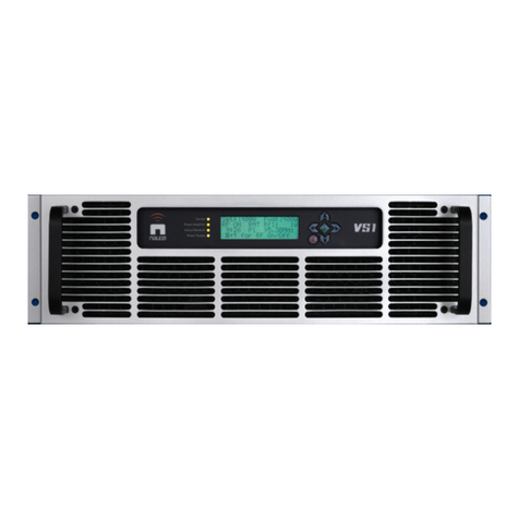
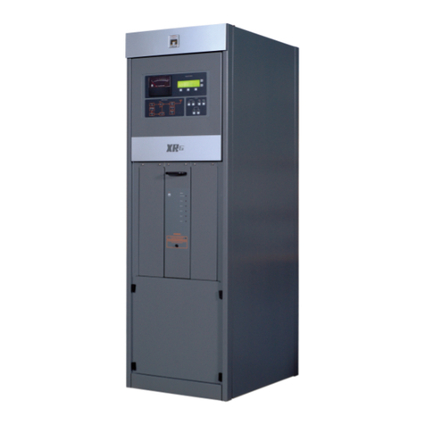
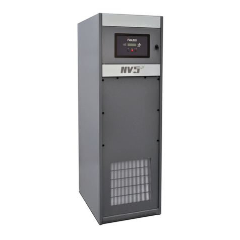
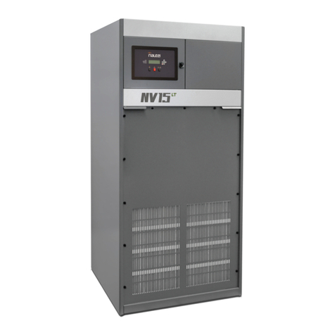
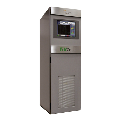
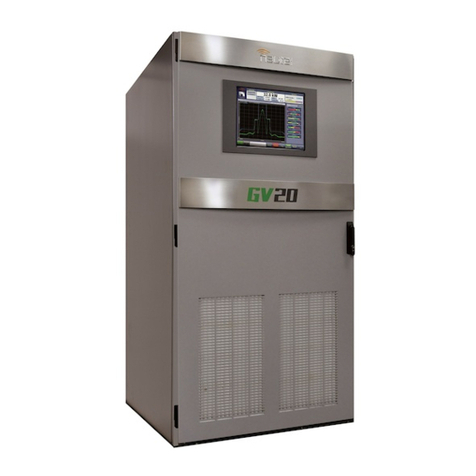
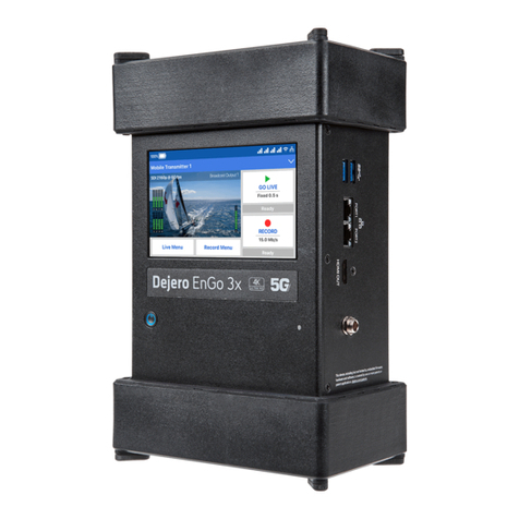
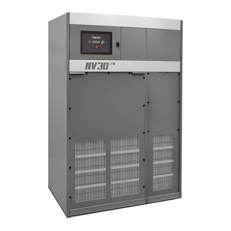
Nautel NV30 User manual

NV30/NV40 Transmitter
Operations and Maintenance
Manual
Document:NHB-NV30-NV40-OPS-3.3
Issue: 3.3 2014-12-10
Status: Standard


Nautel Limited
10089 Peggy’s Cove Road
Hackett’s Cove, NS Canada B3Z 3J4
Phone: +1.902.823.3900 or
Toll Free: +1.877.6NAUTEL (6628835) (Canada & USA only)
Fax: +1.902.823.3183
Nautel Inc.
201 Target Industrial Circle
Bangor, Maine USA 04401
Phone: +1.207.947.8200
Fax: +1.207.947.3693
Customer Service (24 hour support)
+1.877.628.8353 (Canada & USA only)
+1.902.823.5100 (International)
Email: [email protected]
Web: www.nautel.com
The comparisons and other information provided in this document
have been prepared in good faith based on publicly available
information. The reader is encouraged to consult the respective
manufacturer's most recent published data for verification.
© Copyright 2014 NAUTEL. All rights reserved.


NV30/NV40 Operations and Maintenance Manual Table of contents
Page v
Contents
Release control record vii
Description 1-1
Ac-dc power stage 1-2
Control/monitor stage 1-3
RF drive stage 1-4
RF power stage 1-6
Operating the transmitter 2-1
Using the AUI 2-2
Home page 2-14
Menu page - describing transmitter operations 2-15
Logs page - viewing transmitter log 2-16
Viewing tool menu panels 2-25
Viewing real-time meters 2-40
Presets - editing operational settings 2-44
Viewing transmitter status 2-59
Factory Settings 2-61
System Settings 2-70
User accounts 2-79
Changeover page 2-83
User settings 2-84
Remote I/O page 2-104
Routine maintenance 3-1
Scheduled maintenance 3-1
Replacing an air filter 3-3
Performing on-air checks 3-5

NV30/NV40 Operations and Maintenance Manual Table of contents
Page vi Issue 3.3 2014-12-10
Replacing the control/interface PWB battery 3-6
Replacing the NVE exciter PWB battery 3-7
Inspecting lightning protection systems 3-8
Non-standard maintenance 4-1
Upgrading software 4-1
Improving transmitter performance for IBOC presets 4-4
Changing the RF output connector 4-6
Bypassing the UPS interface option 4-11
List of terms 5-1

NV30/NV40 Operations and Maintenance Manual
Issue 3.3 2014-12-10 Page vii
Release control record
Issue Date Reason
3.0 2011-11-10 Release 3 of product (NARF50B)
3.1 2012-12-15 Section 2: updated to support software release 4.0
Section 3: expanded air filter descriptions to include
M7, MERV 7 filters as suitable replacements
3.2 2013-10-01 Added Nautel Phone Home to User Settings
3.3 2014-12-10 Section 2: updated to support software release 4.2.7
or later; changed exciter TCXO screen to show dual
exciter option

NV30/NV40 Operations and Maintenance Manual
Page viii Issue 3.3 2014-12-10

NV30/NV40 Operations and Maintenance Manual Description
Issue 3.3 2014-12-10 Page 1-1
Section 1: Description
Refer to the functional block diagram: NV Series Transmitter Block Diagram - see page 1-9.
This section provides a high-level description of the transmitter’s key sections. The transmitter
circuitry is subdivided into four basic stages:
•Ac-dc power stage
•Control/monitor stage - see page 1-3
•RF drive stage - see page 1-4
•RF power stage - see page 1-6
NV30/NV40 electrical schematics
Some descriptions in this section refer to electrical schematics (SD-#s) . These are located in Section
5 of the NV30/NV40 Troubleshooting Manual.
Redundancy
The NV30/NV40 features redundancy in all key systems:
• RF power modules
• Exciters
• Cooling fans
• Cooling fan power supplies
• Low voltage power supplies
• SBC/AUI power supplies

NV30/NV40 Operations and Maintenance Manual Description
Page 1-2 Issue 3.3 2014-12-10
Ac-dc power stage
See electrical schematics SD-1 (A, Bor C), SD-2 and SD-3.
The ac-dc power stage converts the ac power source to a positive dc voltage (PA volts) for the
transmitter's intermediate (IPA) and RF power amplifiers. The transmitter accepts a wide range of ac
input voltage options:
– 3-phase, 180 - 264 V ac (208 V ac nominal)
– 3-phase, 312 - 457 V ac (380 V ac nominal)
– 1-phase, 180 - 264 V ac (240 V ac nominal)
The ac-dc power stage provides power to operate cooling fans in the power supply modules, RF
power modules and reject load modules. It also provides power to the low voltage power supplies,
which generate the low level dc voltages (±15 V and +5 V) used throughout the transmitter, and to
the +12 V dc power supplies for the SBC (single-board computer) and AUI (advanced user interface).
The ac-dc power stage comprises ac input terminal blocks TB1, TB2 and TB3, an ac distribution
assembly (A6), a power supply distribution PWB (A7), SBC/AUI power supplies A (U1) and B (U2),
LVPS modules A (U3) and B (U4), fan power supply modules A (U7) and B (U8), IPA power supply
modules A (U9), B (U10) and C (U11), and dual PA power supply modules (U12 through U43) for
each of the 16 RF power modules. There is also a PS interface PWB associated with each power
supply module (fan, IPA and PA).
Power supply modules
See Figure SD-2. Power supply modules U9 through U43 convert the ac input voltage to a regulated
dc supply (IPA volts and PA volts) for 16 RF power modules (module contains both IPA and PA).
Each switching power supply module provides 2000 W output, at typical levels of 50 V and 40 A. The
modules regulate the output voltage based on a PA (or IPA) Volts Control input from the control/
monitor stage. Test points on the associated PS interface PWB allow monitoring of module presence
and ac input status. Each module has a built-in cooling fan and each senses out-of-regulation and
excessive temperature conditions and applies PS Fail and PS Temp alarm signals to the associated RF
power module. Both conditions cause the power supply to shut itself down, thus reducing the
transmitter's RF output.
The same modules are used for fan power supply modules U7 and U8. Their PS Fail and PS Temp
alarm signals, as well as the PS Module Present status signal, are applied to the control/monitor stage.
NV30/NV40 Operations and Maintenance Manual Description
Issue 3.3 2014-12-10 Page 1-3
LVPS modules
See Figure SD-1 (A, Bor C). LVPS modules A (U3) and B (U4) convert the ac input voltage to the
regulated low voltage dc supplies. The +5 V, +15 V and -15 V regulated outputs of the supplies are
ORed together at the control/interface PWB (A1) and applied throughout the transmitter.
+12 V power supply modules
See Figure SD-1 (A, Bor C). +12 V power supply modules A (U1) and B (U2) convert the ac input
voltage to the regulated +12 V dc supplies. The +12 V outputs are ORed together on the power
supply distribution PWB (A7) and a common +12 V supply is applied to the control/monitor stage.
Power supply distribution PWB
See Figures SD-1 (A, Bor C) and SD-3. The power supply distribution PWB (A7) interfaces between
fan power supply modules U7 and U8 and the cooling fans for RF power modules 1 through 16 and
reject loads A, B and C. The fan voltage (+48 V) is applied via power rectifiers CR1 and CR2 to the
transmitter's cooling fans. A nominal 47 V is applied as Fan V Sample A and Bto the control/monitor
stage for metering and fan PS fault detection.
The power supply distribution PWB also interfaces between SBC/AUI power supplies U1 and U2
and the control/monitor stage. +12 V is applied via power rectifiers CR3 and CR4 to the control/
monitor stage. A nominal +12 V is applied as +12V Sample A and Bto the control/monitor stage for
metering and supply fault detection.
Control/monitor stage
See electrical schematics SD-4 and SD-5 and Figure 1.1 on page 1-4. The control/monitor stage
monitors critical samples and status/alarm signals from the ac-dc power stage, RF drive stage and RF
power stage. For example, RF power monitoring and RF power stage status information is applied to
the control/monitor stage. Based on the value and status of each input, the control/monitor stage
produces the appropriate control signals for the RF power stage to ensure the proper operation and
protection of the transmitter. The control/monitor stage also provides the remote control/monitor
interface for the transmitter.
The control/monitor stage comprises a control/interface PWB (A1), a remote interface PWB (A2),
an LCD touch monitor (U5) and a single-board computer (U6).
U5 is a 17-inch, colour LCD screen that is mounted on the front of the transmitter. It provides an
advanced user interface (AUI) for the transmitter. The AUI can be controlled by touch screen and is
also available as a flash graphic on any web-interfaced PC or handheld device via the internal NV web
server. See “Using the AUI” on page 2-2 for detailed information on AUI functionality.

NV30/NV40 Operations and Maintenance Manual Description
Page 1-4 Issue 3.3 2014-12-10
The control/interface PWB contains push-button switches that provide backup control for the RF
on/off, local/remote, power increase/decrease and reset functions. It also contains LEDs that serve
as an alternate means to monitor status (local/remote and RF on/off), forward power level
(percentage indicators from 10% to 100% of maximum RF output power) and various alarms.
Figure 1.1: Control/Monitor Stage
RF drive stage
See Figure SD-6. The RF drive stage converts the exciter's RF output to the intermediate RF level
needed to drive the RF power modules. It consists of exciter A (A3), exciter B (A4, optional) and RF
drive splitter/changeover assembly (A5).
Exciter(s)
Refer to the functional block diagram: NVE300 Exciter Block Diagram - see page 1-10.
Exciters A (A3) and B (A4) are the RF drive sources for the transmitter. They accept the external
audio program and/or IBOC information (see the NV30/NV40 Installation Manual for details on
various program input types). The exciters’ main/standby operation is controlled locally using the
AUI, or remotely. The exciter outputs are applied to the RF drive splitter/changeover assembly (A5).
The exciter provides an RF drive signal of 130 W (in analog mode).
From RF Power Stage
From Ac-Dc Power Stage
AUI
To RF Power Stage
To Ac-Dc Power Stage
Control/
Interface
PWB
To RF Drive Stage
From RF Drive Stage
From Remote
Controller To Remote
Monitor
(part of)
Remote
Interface
PWB
(part of)
Remote
Interface
PWB

NV30/NV40 Operations and Maintenance Manual Description
Issue 3.3 2014-12-10 Page 1-5
RF drive splitter/changeover assembly
The RF drive splitter/changeover assembly (A5) controls the routing of the main and standby
exciters and provides the RF drive signals for the 16 RF power modules. The assembly is comprised
of the splitter/changeover PWB (A5A1), two 4-way RF drive splitter PWBs (A2 and A3), two
attenuator PWBs (A4 and A5) and eight 3 dB hybrid couplers (U1 through U8).
Exciter relay control
The RF drive outputs from exciters A and B are applied to the splitter/changeover PWB (A5A1) at
A5A1J1 and A5A1J2 respectively. The Exciter Relay Control input (A5A1J3-4) is a signal applied from
the control/monitor stage that controls relay A5A1K1.
• When exciter A is selected as the main RF drive source, the Exciter Relay Control input is open
circuit and relay A5A1K1 will be de-energized. Exciter A's output will be applied to 3 dB
hybrid coupler A5A1U1.
• When exciter B is selected as the main RF drive source, the Exciter Relay Control input is near
ground potential (0 V) and relay A5A1K1 will be energized. Exciter B's output will be
applied to 3 dB hybrid coupler A5A1U1.
Exciter drive splitter
The splitter/changeover PWB’s 3 dB hybrid coupler (A5A1U1) is connected as a splitter. The RF
drive source (A or B) selected by relay A5A1K1 is applied to A5A1U1’s input. The signal is split into
two equal amplitude signals that are 90° out-of-phase. These split signals are applied to 4-way RF
drive splitter PWBs A5A2 and A5A3.
4-way RF drive splitter
Each 4-way RF drive splitter PWB (A5A2 and A5A3) accepts an output from the exciter 3 dB hybrid
coupler and splits it into four equal amplitude signals, using three 3 dB couplers identical to A5A1U1.
The outputs of each 4-way RF drive splitter are applied to the final RF drive splitters.
Final RF drive splitters
3 dB hybrid couplers A5U1 through A5U8 (identical to A5A1U1) are connected as splitters. Each
coupler accepts an output of the 4-way RF drive splitters and splits the signal into two equal
amplitude signals that are 90° out-of-phase. These split signals are applied to attenuator PWB A5A4
and A5A5.
Attenuators
The attenuator PWBs (A5A4 and A5A5) accepts the outputs from the 4-way RF drive splitter PWBs
and attenuate each of the signals for application to the 16 RF power modules. Attenuation values are
set in order to balance the RF drive output levels.

NV30/NV40 Operations and Maintenance Manual Description
Page 1-6 Issue 3.3 2014-12-10
RF power stage
See Figures SD-7, SD-8 and SD-9. The RF power stage accepts the intermediate RF drive inputs from
the RF drive stage and generates the final RF output. It consists of 16 RF power modules, four
module backplane PWBs (A17, A32, A50 and A65), four 10 kW combiner/filters (A16, A31, A49
and A64), two 20 kW combiners (A30 and A63), a 40 kW combiner (A48), an output power probe
(A13), three reject load assemblies [A (A14, 8-input), B (A45, 4-input) and C (A46, 4-input)] and two
reject load interface PWBs [A (A15) and B (A47)].
RF power module
See Figure SD-7 (see the NV30/NV40 Troubleshooting Manual for a detailed RF power module
description) and “RF Power Module Block Diagram” on page 1-11.
Each of the 16 RF power modules provides up to 2750 W (for NV40) or 2062.5 W (for NV30) of RF
output power and is comprised of an IPA power amplifier PWB, eight power amplifier PWBs, power
module interface PWB, combiner PWB, splitter PWB and six cooling fans. The intermediate RF drive
outputs from the RF drive stage are applied to the RF power modules via module backplane PWBs 1-
4 (A17), 5-8 (A32), 9-12 (A50) and 13-16 (A65). Within each RF power module, the intermediate RF
drive signal is sampled and then drives the IPA amplifier. The IPA output is sampled then split to
drive the module's eight PAs. The IPA Volts and PA Volts inputs from the associated switching power
supply modules control the RF output of the IPA and eight PAs, respectively. The RF power module
receives alarm and status signals (PS Temp, PS Fail, PS AC Fail, and PS Module Present) from the ac-dc
power stage. The RF power module also provides a Pwr Supply Inhibit signal (one for each of the
power module’s dual supplies) to the ac-dc power stage, which, when active, inhibits the associated
switching power supply. A PA V Sample and IPA V sample from each RF power module is applied to
the control/monitor stage. The control/monitor stage supplies a PA Volts Inhibit signal, which
controls the PA outputs of the RF power module.
Module backplane PWB
See Figure SD-7. Each set of four RF power modules (1-4, 5-8, 9-12 and 13-16) has an associated
module backplane PWB which interfaces with all module inputs and outputs, except for the RF
output. It also provides the fan volts connections for the module's cooling fans. The setting of
dipswitches S1 through S4 assign a four-bit address for each specific module based on module
position. Jumper E1 is set to TERM on RF power module 16 (the last module) to terminate the RS-
485 serial communication cable.
Combiner/filters
See Figure SD-8. There are various stages of combiners used in the transmitter. All combining
follows a corporate (or binary) structure in that pairs of RF power blocks are combined throughout
the RF chain from the RF power modules to the RF output.

NV30/NV40 Operations and Maintenance Manual Description
Issue 3.3 2014-12-10 Page 1-7
10 kW combiner/filters
Each 10 kW combiner/filter (A16, A31, A49 and A64) is a 2-stage combiner that accepts the RF
outputs from four RF power modules and provides a single RF output. Each 10 kW combiner/filter
uses three 3 dB hybrid couplers - two of which are used in the initial pair of 5 kW combiners, which
each accept the outputs of two RF power modules. The equal amplitude, 90° out-of-phase
(quadrature) RF signals are combined at the 3 dB hybrid coupler outputs and applied to a third and
final, 10 kW 3 dB hybrid coupler. Again, the equal amplitude, quadrature RF signals are combined.
The combined output is applied to a 10 kW low pass filter before being applied to a 20 kW combiner.
Any amplitude or phase imbalances between 3 dB hybrid coupler inputs cause a proportional signal
to be applied to the applicable reject load assemblies. The amplitude of the 5 kW Rej Ld Pwr signals
(via J5 and J6) represents imbalance between the combined outputs of the first stage of combining.
The amplitude of the 10 kW Rej Ld Pwr signal (via J7) represents imbalance between the combined
outputs of the second stage of combining (differences in pairs of RF power modules).
20 kW combiners
The 20 kW combiners (A30 and A63), which are hybrid couplers, accept the RF outputs from the
10 kW combiner/filters. The equal amplitude, 90° out-of-phase (quadrature) RF signals are combined
at hybrid coupler outputs and applied to the 40 kW combiner.
Any amplitude and phase imbalances between the inputs of the 20 kW combiners causes a
proportional signal to be applied (via J1) to the applicable reject load assemblies. The amplitude of
the 20 kW Rej Ld Pwr signals represents imbalance between the combiner inputs.
40 kW combiner
The 40 kW combiner (A48), which is a hybrid coupler, accepts the RF outputs from the 20 kW
combiners. The equal amplitude, 90° out-of-phase (quadrature) RF signals are combined at the hybrid
coupler output and applied to the output power probe.
Any amplitude and phase imbalances between the inputs of the 40 kW combiner causes a
proportional signal to be applied (via J1) to the applicable reject load assembly. The amplitude of the
40 kW Rej Ld Pwr signal represents imbalance between the combiner inputs.
Output power probe
See Figure SD-8. The output power probe (A13) monitors the transmitter's forward and reflected
power and generates the Fwd Pwr Sample (A1J1) and Refld Pwr Sample (A2J1) signals applied to the
control/monitor stage for protection and monitoring. RF monitor PWB A3 provides a nominal 4.5 V
(NV40) or 3.7 (NV30) rms [at 40 kW (NV40) or 30 kW (NV30) signal at A3J1 for use with a

NV30/NV40 Operations and Maintenance Manual Description
Page 1-8 Issue 3.3 2014-12-10
modulation monitor or spectrum analyzer. RF sample PWBs A4 and A5 provide similar samples at
A4J1 and A5J1. These samples are applied to exciters A and B (if used) for use by the exciters'
adaptive pre-correction circuitry [for all-digital (HD) or hybrid (FM+HD) modes of operation] and
also by the AUI’s spectrum analyzer display.
Reject load assemblies
See Figure SD-9. Reject load assemblies provide a means to dissipate reject power from the outputs
of the combiner/filter's 3 dB hybrid couplers. Reject load assemblies contain power resistors to
dissipate reject power and cooling fans to regulate temperature. There are three different reject load
assemblies (A, B and C) used in the transmitter.
8-input reject load assembly ‘A’
Reject power generated by the 5 kW combining stage of any of the four 10 kW combiner/filter
assemblies is dissipated by resistors in 8-input reject load assembly ‘A’ (A14). Micro-strip transmission
lines (on 8-input reject load PWB A14A1) in close proximity to the reject load signals induce eight
true RF sample voltages of the associated reject power. These samples are peak detected and applied
to the control/monitor stage via reject load interface PWB ‘A’ (A15). The reject load interface PWB
provides an interface between the ac-dc power stage’s Fan Volts supply and the reject load assembly’s
cooling fans. It also acts as the interface between the cooling fans’ Rej Fan Tach signals and the
control/monitor stage.
4-input reject load assembly ‘B’
Reject power generated by the output combining stage of any of the four 10 kW combiner/filter
assemblies is dissipated by resistors in 4-input reject load assembly ‘B’ (A45). Micro-strip
transmission lines (on 4-input reject load PWB A45A1) in close proximity to the reject load signals
induce four true RF sample voltages of the associated reject power. These samples are peak detected
and applied to the control/monitor stage via reject load interface PWB ‘B’ (A47). The reject load
interface PWB provides an interface between the ac-dc power stage’s Fan Volts supply and the reject
load assembly’s cooling fans. It also acts as the interface between the cooling fans’ Rej Fan Tach signals
and the control/monitor stage.
4-input reject load assembly ‘C’
Reject power generated by the output combining stage of either of the two 20 kW combiners or the
40 kW combiner is dissipated by resistors in 4-input reject load assembly ‘C’ (A46). Micro-strip
transmission lines (on 4-input reject load PWB A46A1) in close proximity to the reject load signals
induce three true RF sample voltages of the associated reject power. These samples are peak detected
and applied to the control/monitor stage via reject load interface PWB ‘B’ (A47). The reject load
interface PWB provides an interface between the ac-dc power stage’s Fan Volts supply and the reject
load assembly’s cooling fans. It also acts as the interface between the cooling fans’ Rej Fan Tach signals
and the control/monitor stage.
NV30/NV40 Operations and Maintenance Manual
Issue 3.3 2014-12-10 Page 1-9
Figure 1.2: NV Series Transmitter Block Diagram
FAN
PWR
IPA
C1
A1
PA4
PA3
PA2
PA1
C2
A2
PWR
REJ
PWR
REJ
PWR
PWR IPA
FWD
D1
B1
PA8
PA5
PA6
PA7
D2
B2
FWD
AUI
PWR
REMOTE CONTROL/
AC POWER
240VAC
AC POWER
208VAC
OR
3 PHASE
AC POWER
B
A
B
IPA
PWR
EXCTR
SUPPLY
SUPPLY
SBC/AUI
SUPPLY
PWR SUPPLY
MODULE C
MODULE A
PWR
REJ
PWR
PWR
FILTER
REJ
PWR
PWR
PROBE
POWER
MONITORING
1 PHASE
OR
3 PHASE
400VAC
A
SUPPLY
LV PWR
IPA
C
LV PWR
IPA
A
FWD
LV PWR
IPA PWR SUPPLY
PWR SUPPLY
PWR SUPPLY
PWR SUPPLY
SPLITTER
MODULE D
MODULE B
COMBINER
REFLD
SBC
REJ
REJ
OUTPUT
B2060004 VE
FAN PWR SUPPLY
EXCITER B IPA PWR SUPPLY
EXCITER A
INTEGRAL EXCITER
FAN PWR SUPPLY
(OPTIONAL)
SUPPLY B
(OPTIONAL)
SBC/AUI PWR
SUPPLY B
(OPTIONAL)
PWR SUPPLY
PWR SUPPLY
SBC/AUI PWR SUPPLY
10KW POWER BLOCK
10KW POWER BLOCK
10KW POWER BLOCK
PWR SUPPLY
10KW POWER BLOCK
RF OUTPUT
(OPTIONAL)
IPA PWR SUPPLY
FAN PWR SUPPLY
16 WAY
SPLITTER
IPA PWR SUPPLY
FAN PWR SUPPLY
FAN SUPPLY
FAN SUPPLY
IPA PWR SUPPLY
SBC/AUI PWR
PWR SUPPLY
SUPPLY A
LV PWR SUPPLY
SYSTEM CONTROL
PWR SUPPLY
PWR SUPPLY
PWR SUPPLY
LOW PASS

NV30/NV40 Operations and Maintenance Manual
Issue 3.3 2014-12-10 Page 1-10
Figure 1.3: NVE300 Exciter Block Diagram
DAC
ADC
ADC
I/O
ADC
SUPPLY
PILOT/MPX SAMPLE
REMOTE INTERFACE
CONSOLE
COMPOSITE SCA
MPX
L/R
SCA GENERATOR
2 x AES/EBU
TOSLINK OPTICAL
EXTERNAL 10MHz REFERENCE
FPGA
TCXO OR
OCXO
EXCITER PWB
RF DAC
PLL & VCSO
FILTER &
PREAMP
BIAS
DAC
BIAS
POWER
VSWR
PROTECTION
FILTER
(OPTIONAL)
RF OUT
B2060001 VA
AC/DC
DSP
LINEAR
REGULATOR
PROBES
HARMONIC
SUPPLY
RS232
RF SAMPLE (-30dBc)
TEMP SENSE
POWER AMPLIFIER
85-264VAC DC/DC
REGULATED
ASRC

NV30/NV40 Operations and Maintenance Manual
Issue 3.3 2014-12-10 Page 1-11
Figure 1.4: RF Power Module Block Diagram
FWD FWD
6
4
1
4-WAY
PWR PWR
7
8
5
2
3
4-WAY
SPLITTER
4-WAY COMBINER
FWD
PWR
OUTPUT
B2060005 VB
IPA 4-WAY
SPLITTER COMBINER
PWR SUPPLY 1
IPA PWR SUPPLY
PWR SUPPLY 2
RF DRIVE

NV30/NV40 Operations and Maintenance Manual Operating the transmitter
Issue 3.3 2014-12-10 Page 2-1
Section 2: Operating the transmitter
This section provides information about operating the NV30/NV40 transmitter:
•Using the AUI - see page 2-2
•Home page - see page 2-14
•Menu page - describing transmitter operations - see page 2-15
•Logs page - viewing transmitter log - see page 2-16
•Viewing tool menu panels - see page 2-25
•Viewing real-time meters - see page 2-40
•Presets - editing operational settings - see page 2-44
•Viewing transmitter status - see page 2-59
•Factory Settings - see page 2-61
•System Settings - see page 2-70
•User accounts - see page 2-79
•Changeover page - see page 2-83
•User settings - see page 2-84
•Remote I/O page - see page 2-104
This manual suits for next models
3
Table of contents
Other Nautel Transmitter manuals

Nautel
Nautel NX200 User manual

Nautel
Nautel XR6 User manual

Nautel
Nautel VX150 User manual

Nautel
Nautel NV40 Programming manual

Nautel
Nautel VS300 User manual

Nautel
Nautel XL12 Owner's manual

Nautel
Nautel XR12 Programming manual

Nautel
Nautel VS2.5 User manual

Nautel
Nautel FM10011 User manual

Nautel
Nautel NV10LT User manual
Popular Transmitter manuals by other brands

MSA
MSA General Monitors S4100T instruction manual

Emerson
Emerson Rosemount 2088 Reference manual

SUTO
SUTO S217 Instruction and operation manual

Extron electronics
Extron electronics PowerCage FOX 4G Tx VGA user manual

Honeywell
Honeywell 5804 - Ademco Wireless Key installation guide

COBHAM
COBHAM M2TE-S Operation manual