Nokia HSU-1 - Cell Phone Car Handset Guide

After Sales Technical Documentation
Original 50/96 NMP Part No. 0275276
Handset HSU–1

After Sales
Technical Documentation
Handset HSU–1
Page – 2 Original 50/96
CONTENTS
Handset HSU–1 – 3. . . . . . . . . . . . . . . . . . . . . . . . . . . . . . . . . . . . . . . .
Introduction – 3. . . . . . . . . . . . . . . . . . . . . . . . . . . . . . . . . . . . . . . . . .
Technical Summary – 3. . . . . . . . . . . . . . . . . . . . . . . . . . . . . . . .
Use of Handset – 3. . . . . . . . . . . . . . . . . . . . . . . . . . . . . . . . . . . .
Technical Specifications – 4. . . . . . . . . . . . . . . . . . . . . . . . . . . . . . .
Modes of Operation – 4. . . . . . . . . . . . . . . . . . . . . . . . . . . . . . . .
Maximum Ratings – 4. . . . . . . . . . . . . . . . . . . . . . . . . . . . . . . . . .
DC Characteristics – 4. . . . . . . . . . . . . . . . . . . . . . . . . . . . . . . . .
AC Characteristics – 4. . . . . . . . . . . . . . . . . . . . . . . . . . . . . . . . .
Microphone Side – 4. . . . . . . . . . . . . . . . . . . . . . . . . . . . . . . . .
Earphone Side – 4. . . . . . . . . . . . . . . . . . . . . . . . . . . . . . . . . .
Sidetone – 4. . . . . . . . . . . . . . . . . . . . . . . . . . . . . . . . . . . . . . . .
External Signals and Connections – 5. . . . . . . . . . . . . . . . . .
External Connections – 5. . . . . . . . . . . . . . . . . . . . . . . . . . . . . . .
Functional Description – 5. . . . . . . . . . . . . . . . . . . . . . . . . . . . . . . .
Circuit Description – 5. . . . . . . . . . . . . . . . . . . . . . . . . . . . . . . . . .
Earphone Amplifier – 6. . . . . . . . . . . . . . . . . . . . . . . . . . . . . . .
Microphone Amplifier – 6. . . . . . . . . . . . . . . . . . . . . . . . . . . . .
HOOK Operation – 6. . . . . . . . . . . . . . . . . . . . . . . . . . . . . . . .
Voltage Regulator – 7. . . . . . . . . . . . . . . . . . . . . . . . . . . . . . . .
Block Diagram – 7. . . . . . . . . . . . . . . . . . . . . . . . . . . . . . . . . . . . . . .
Circuit Diagram version 6.0 – 8. . . . . . . . . . . . . . . . . . . . . . . . . . . .
Layout Diagrams – 9. . . . . . . . . . . . . . . . . . . . . . . . . . . . . . . . . . . . .
Parts List of DG1 (Version 1.1) Code 0200221 – 10. . . . . . . . .
Exploded view – 12. . . . . . . . . . . . . . . . . . . . . . . . . . . . . . . . . . . . . . .
Assembly parts – 12. . . . . . . . . . . . . . . . . . . . . . . . . . . . . . . . . . . . . . .

After Sales
Technical Documentation Handset HSU–1
Page – 3
Original 50/96
Handset HSU–1
Introduction
Main function of the HSU–1 Audio Handset is to form an electroacoustic
interface between the user and the phone environment.
Technical Summary
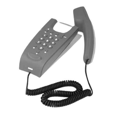
The HSU–1 Audio Handset consists of handset with coil cord and of
cradle. In the handset there is earphone and microphone with corre-
sponding amplifiers. There is also a simply interface for controlling these
functions. Electronics consist of DG–1 handset module. Mechanical di-
mensions are small and mechanics consists of A–cover, B– cover and coil
cord with the cradle. The HSU–1 Audio Handset has a volume potentiom-
eter.
Use of Handset
The HSU–1 Audio Handset is designed to be a dummy handset with no
display and no keyboard. Its use is to form an electroacouistical connec-
tion between the user and DCT – environment. When not in use the
handset is on the cradle. During the use the handset is lifted from the
cradle and audio paths are opened.

After Sales
Technical Documentation
Handset HSU–1
Page – 4 Original 50/96
Technical Specifications
Modes of Operation
DG–1 module has only one mode of operation. Audio paths will become
active when the handset is lifted from the cradle. Otherwise muting is on.
Maximum Ratings
–supply voltage: 16.0 V
–operation temperature range, specification: – 25 ––– + 55 C
–operation temperature range, operational: – 25 ––– + 85 C
–storage temperature range: – 40 ––– + 85 C
DC Characteristics
Symbol Parameter Minimum Typical/ Maximum
Nominal
VBS Supply voltage for electronics 9.0 V 13.2 V 16.0 V
Ihs Handset current consumption 6.0 mA 8.0 mA 12.0 mA
Vaudio Regulated audio voltage 7.7 V 8.3 V 8.7 V
Iaudio Audio current consumption 6.0 mA 8.0 mA 12.0 mA
AC Characteristics
Microphone Side
Microphone amplifier gain for nominal signal is approx. 30 dB. Max output
level is 1 Vrms. Idle noise of microphone amplifier should be less than
–64 dBmOp (220 uV). Output impedance is < 300 ohms.
Earphone Side
Earphone amplifier input level is max. 503 mVrms. Acoustic idle noise of
earphone is under –60 dBPa. Input impedance of earphone amplifier is >
10 kohm.
Sidetone
To be defined later.

After Sales
Technical Documentation Handset HSU–1
Page – 5
Original 50/96
External Signals and Connections
The HSU–1 Audio Handset has an 8 pin modular connector at the end of
the coil cord to the junction box. There are only five lines in use in the coil
cord.
External Connections
Functional Description
Main function of The HSU–1 Audio Handset is to form an electroacoustic
interface between the user and the phone environment. The HSU–1 Au-
dio Handset consists of handset with coil cord and of cradle. In the hand-
set there is earphone and microphone with corresponding ampli-
fiers.There is also a simply interface for controlling these functions. Elec-
tronics consist of DG1 handset module. Mechanical dimensions are small
and mechanics consists of A–cover, B–cover and coil cord with the
cradle. The HSU–1 Audio Handset has a volume potentiometer.
Circuit Description
HSU–1 Audio Handset consists of the following functional blocks:
– Earphone amplifier
– Microphone amplifier

After Sales
Technical Documentation
Handset HSU–1
Page – 6 Original 50/96
– HOOK switch ( REED relay )
– Voltage regulator
Earphone and microphone paths are controlled by Hook switch, which is
opened automatically, when the handset is lifted from the cradle. In the
cradle there is a magnet and in the handset there is a reed relay. Reed
relay controls audio switches. The earphone amplifier is differential type
and output is symmetrical. Volume is user controllable. Microphone is an
electret microphone (condensator type) with field effect transistor. It re-
quires a bias voltage above 2.0 Volts for normal operation. Bias voltage is
generated with suitable deviding resistors and transistor from regulated
8.5 V.
Earphone Amplifier
Earphone amplifier is of differential type. N2A and N2B are used to form a
differential amplifier with total amplification of 26 dB. Ear signal is fed to
DG–1 module via connector X1 pin 8. L2 and C3 are used to improve
EMI characteristics. Capacitor C5 blocks DC of the signal analog switch
N3A ( 74HC4066 ) switches Ear signal during ON HOOK state. Capacitor
C24 is used to modificate frequency characteristics of Ear signal at higher
frequencies. The gain of ear piece amplifier is set by resistors R14, R15,
R16 and R17, R18. R19 is used to form side tone. Ear piece capsule is
connected to the PC–board via connector X2. Resistors R20, R23, R26
and trimmer R22 attenuates Ear signal. Attenuation is about 20 dB when
the trimmer is at minimum position.
Microphone Amplifier
Transistor V1 supplies bias voltage to Microphone. Bias voltage is filtered
by C20, C11,C12, C14 and resistors R12, R13. Bias voltage is fed to mi-
crophone connector X3 via resistor R11. Bias voltage at connector X3 pin
1 is about 3.4 volt. Capacitor C10 blocks DC voltage of the Mic signal. Mic
signal is amplified by N2D ( TL074ID ) Resistors R5, R7, R8, R9, R10 and
capacitor C7, C9, C15 are used to filter Mic signal. Capacitor C8, C16,
C23 are used to improve EMI characteristics. Gain of Mic amplifier is set
by R7 and R24. Mic signal is fed to Ear amplifier via resistor R19 to form
side tone signal. Mic signal is fed to connector X1 pin 7 via analog switch
N3B ( 74HC4066 ). Capacitor C19 blocks DC voltage of the signal.
HOOK Operation
Both Mic signal and Ear signal are controlled by analog switches
74HC4066. Audio channels are open when Reed relay S1 is not acti-
vated. S1 is connected to Enable inputs of analog switches and R5 is a
pull– up resistor to open analog switches when S1 is open. When S1 is
activated ( is closed ) analog switches are opened. Resistor R21 and ca-
pacitor C21 forms a filter to improve EMI characteristics.
After Sales
Technical Documentation Handset HSU–1
Page – 7
Original 50/96
Voltage Regulator
Supply voltage to DG–1 module is fed via connector X1 pin 1. Voltage is
regulated with regulator N1 ( LP2951 ACM ). Capacitors C4 and C1 are
used to improve filtering. Bias voltage for Mic and Ear signals and amplifi-
ers is made byamplifier N2C (TL074ID). Regulated voltage 5 volts is de-
vided by resistors R1 and R2 and the amplified by N2C. Capacitor C18
filters regulated voltage.
Block Diagram

After Sales
Technical Documentation
Handset HSU–1
Page – 8 Original 50/96
Circuit Diagram version 6.0

After Sales
Technical Documentation Handset HSU–1
Page – 9
Original 50/96
Layout Diagrams

After Sales
Technical Documentation
Handset HSU–1
Page – 10 Original 50/96
Parts List of DG1 (Version 1.1) Code 0200221
ITEM CODE DESCRIPTION VALUE TYPE
R001 1414036 Chip resistor 8.2 k 5 % 0.1 W 0805
R002 1412430 Chip resistor 10 k 5 % 0.1 W 0805
R003 1413635 Chip resistor 100 k 5 % 0.1 W 0805
R004 1413635 Chip resistor 100 k 5 % 0.1 W 0805
R005 1414029 Chip resistor 3.3 k 5 % 0.1 W 0805
R006 1412261 Chip resistor 100 5 % 0.1 W 0805
R007 1414109 Chip resistor 15 k 5 % 0.1 W 0805
R008 1414109 Chip resistor 15 k 5 % 0.1 W 0805
R009 1414109 Chip resistor 15 k 5 % 0.1 W 0805
R010 1414109 Chip resistor 15 k 5 % 0.1 W 0805
R011 1414029 Chip resistor 3.3 k 5 % 0.1 W 0805
R012 1412729 Chip resistor 33 k 5 % 0.1 W 0805
R013 1412609 Chip resistor 27 k 5 % 0.1 W 0805
R015 1413723 Chip resistor 470 k 5 % 0.1 W 0805
R016 1414029 Chip resistor 3.3 k 5 % 0.1 W 0805
R018 1413723 Chip resistor 470 k 5 % 0.1 W 0805
R019 1413723 Chip resistor 470 k 5 % 0.1 W 0805
R020 1412254 Chip resistor 270 5 % 0.1 W 0805
R021 1414029 Chip resistor 3.3 k 5 % 0.1 W 0805
R022 1703319 Tpmet 0w5 2k2 m
R024 1414004 Chip resistor 680 5 % 0.1 W 0805
R025 1413635 Chip resistor 100 k 5 % 0.1 W 0805
R026 1412409 Chip resistor 1.5 k 5 % 0.1 W 0805
R027 1414406 Chip resistor 5.6 k 5 % 0.1 W 0805
R028 1412729 Chip resistor 33 k 5 % 0.1 W 0805
R029 1412536 Chip resistor 22 k 5 % 0.1 W 0805
R030 1412261 Chip resistor 100 5 % 0.1 W 0805
R031 1412261 Chip resistor 100 5 % 0.1 W 0805
R032 1412173 Chip resistor 33 5 % 0.1 W 0805
C001 2307816 Ceramic cap. 47 n 20 % 25 V 0805
C002 2307816 Ceramic cap. 47 n 20 % 25 V 0805
C003 2310336 Ceramic cap. 18 p 5 % 50 V 0805
C004 2310336 Ceramic cap. 18 p 5 % 50 V 0805
C005 2310784 Ceramic cap. 100 n 10 % 25 V 0805
C006 2310336 Ceramic cap. 18 p 5 % 50 V 0805
C007 2310738 Ceramic cap. 4.7 n 20 % 50 V 0805
C008 2310336 Ceramic cap. 18 p 5 % 50 V 0805
C009 2310752 Ceramic cap. 10 n 20 % 50 V 0805
C010 2307816 Ceramic cap. 47 n 20 % 25 V 0805
C011 2310336 Ceramic cap. 18 p 5 % 50 V 0805
C012 2310336 Ceramic cap. 18 p 5 % 50 V 0805
C013 2310512 Ceramic cap. 560 p 5 % 50 V 0805
C014 2310512 Ceramic cap. 560 p 5 % 50 V 0805

After Sales
Technical Documentation Handset HSU–1
Page – 11
Original 50/96
C015 2310544 Ceramic cap. 1.0 n 5 % 50 V 0805
C016 2310336 Ceramic cap. 18 p 5 % 50 V 0805
C017 2604431 Tantalum cap. 10 u 20 % 16 V 6.0x3.2x2.5
C018 2604209 Tantalum cap. 1.0 u 20 % 16 V 3.2x1.6x1.6
C019 2604431 Tantalum cap. 10 u 20 % 16 V 6.0x3.2x2.5
C020 2604209 Tantalum cap. 1.0 u 20 % 16 V 3.2x1.6x1.6
C021 2307816 Ceramic cap. 47 n 20 % 25 V 0805
C022 2604431 Tantalum cap. 10 u 20 % 16 V 6.0x3.2x2.5
C023 2310336 Ceramic cap. 18 p 5 % 50 V 0805
C024 2310512 Ceramic cap. 560 p 5 % 50 V 0805
C025 2310752 Ceramic cap. 10 n 20 % 50 V 0805
C026 2310336 Ceramic cap. 18 p 5 % 50 V 0805
C027 2310784 Ceramic cap. 100 n 10 % 25 V 0805
C028 2310336 Ceramic cap. 18 p 5 % 50 V 0805
C029 2310336 Ceramic cap. 18 p 5 % 50 V 0805
C030 2310512 Ceramic cap. 560 p 5 % 50 V 0805
C031 2310336 Ceramic cap. 18 p 5 % 50 V 0805
C032 2310512 Ceramic cap. 560 p 5 % 50 V 0805
C033 2310512 Ceramic cap. 560 p 5 % 50 V 0805
C034 2310512 Ceramic cap. 560 p 5 % 50 V 0805
C035 2310512 Ceramic cap. 560 p 5 % 50 V 0805
C036 2310512 Ceramic cap. 560 p 5 % 50 V 0805
C037 2310512 Ceramic cap. 560 p 5 % 50 V 0805
L001 3608502 Chip coil 5 % Q=28/35 MHz 1206
L002 3608502 Chip coil 5 % Q=28/35 MHz 1206
V001 4200917 Transistor BC848B/BCW32 npn 30 V 100 mA SOT23
V002 4110140 Zener diode BZX84 5 % 6.8 V 0.3 W SOT23
V003 4110140 Zener diode BZX84 5 % 6.8 V 0.3 W SOT23
V004 4110140 Zener diode BZX84 5 % 6.8 V 0.3 W SOT23
N001 4301062 IC, regulator LP2951AC SO8S
N002 4306494 IC, 2 x op.amp. TL074ID SO14
N003 4309488 IC, 4 x bi.switch 74HC4066 SO14S
S001 5304759 Reed relay 10at 0.5a 2x15 smd
X001 5416638 Connector 8–pole right angle 1.5 1.5
X002 5416640 Pin header m1x2 p1.5 90deg 1a0r02 1A0R02
9854017 PCB DG1 30.0X72.0X1.0 M2 6/PA
9854017 PC board DG1 30.0x72.0x1.0 m2 6/pa

After Sales
Technical Documentation
Handset HSU–1
Page – 12 Original 50/96
Exploded view
Assembly parts
ITEM Q’TY CODE DESCRIPTION VALUE, TYPE
1 9450302 Front cover 2D 23151 HSU–1
2 9459393 Bottom cover 2D 23152 HSU–1
3 9450132 Mic spacer 4D 21588 NHE–2
4 9450133 Earphone spacer 4D 21596 NHE–2
5 9450304 Cradle cover 2D 23153 HSU–1
6 9450305 Cradle bottom 2D 23154 HSU–1
8 9460098 Latch 3D 23155 HSU–1
9 9780086 Coil cord 4C 22857 HSU–1
10 6490220 Magnet 4D 21413 CRE–1
11 7313054 Magnet pad 4D 21422 CRE–1
12 9560015 Spring 4D 23498 HSU–1
13 9560001 Spindle 4D 21412 CRE–1
14 2 9480171 D shape sealing 4D 24417
15 6 6154430 PT screw KB25x8 FeZn clr
16 9380154 Label blank 4D 22419 23.8x17.5
16 9380154 Label HSU–1 4D 23481
16 9380154 Label HSU–1A 4D 24526
16 9380154 Label HSU–1P 4D 24591
17 9450075 Rubber pad 4D 21562

After Sales
Technical Documentation Handset HSU–1
Page – 13
Original 50/96
18 5140379 Cond. microphone 62 ±3 dB 2.2 kΩ6x5
19 5140578 Receiver capsule 103 ±2 dB
20 9510193 Earpiece clip 4D 24147
21 6291917 PT screw KB25x5 FeZn clr
H1 0200221 Handset module DG–1

After Sales
Technical Documentation
Handset HSU–1
Page – 14 Original 50/96
[This page intentionally left blank]
Table of contents
Other Nokia Telephone manuals

Nokia
Nokia 6610i - Cell Phone 4 MB User manual

Nokia
Nokia 6300 4G User manual

Nokia
Nokia 515 RM-953 User manual

Nokia
Nokia 1208 User manual

Nokia
Nokia 5310 XpressMusic User manual

Nokia
Nokia 2780 Flip User manual

Nokia
Nokia N97 User manual

Nokia
Nokia 2780 Flip User manual

Nokia
Nokia HF-510 User manual

Nokia
Nokia 1110 User manual