Portwell PEB-1431V User manual

PEB-1431V
Embedded System Board
User’s Manual
P/N: B8980770 Version 1.0
Copyright © Portwell, Inc., 2002. All rights reserved.
All other brand names are registered trademarks of their respective owners.

Preface
EC Declaration of Conformity
(To Be Added)
For the following equipment:
Product Name:
Model Name:
Trade Name:
is herewith confirmed to comply with the requirements set out in the Council
Directive on the Approximation of the Laws of the Member States relating to
Electromagnetic Compatibility Directive (89/336/EEC). The equipment was
evaluated and passed the test, the following standards were applied :
EMC : EN 55022 (1994/A1:1995 Class A)
EN 50082-2 (1991)
EN 61000-4-2 (1995)
EN 61000-4-3 (1996)
EN 61000-4-4 (1995)
EN 61000-3-2 (1995)
EN 61000-3-3 (1995)
The following manufacturer is responsible for this declaration :
Portwell, Inc.
(Company Name)
3F, No.88, Sec.1, Nei-Hu Rd., Taipei, Taiwan, R.O.C.
(Company Address)
Taipei, R.O.C.
Place Date Legal Signature of
Authorized Person

Preface
Table of Contents
How to Use This Manual
Chapter 1 System Overview.......................................................................................................1-1
1.1 Introduction................................................................................................................................. 1-1
1.2 Check List .................................................................................................................................... 1-2
1.3 Product Specifications................................................................................................................ 1-2
1.3.1 Mechanical and Environmental ...................................................................................... 1-4
1.3.2 Mechanical Drawing......................................................................................................... 1-4
1.4 System Architecture ................................................................................................................... 1-5
1.4.1 TPC Atlas............................................................................................................................ 1-5
1.4.2 STPC Atlas Integrated Graphics...................................................................................... 1-5
1.4.3 PC/104 Interface................................................................................................................ 1-5
1.4.4 SDRAM Interface............................................................................................................... 1-5
1.4.5 IDE Interface ...................................................................................................................... 1-5
1.4.6 STPC Atlas and Winbond W83977F-A........................................................................... 1-6
1.4.7 Compact Flash Interface...................................................................................................1-6
Chapter 2 Hardware Configuration ...........................................................................................2-1
2.1 Jumper Setting............................................................................................................................. 2-1
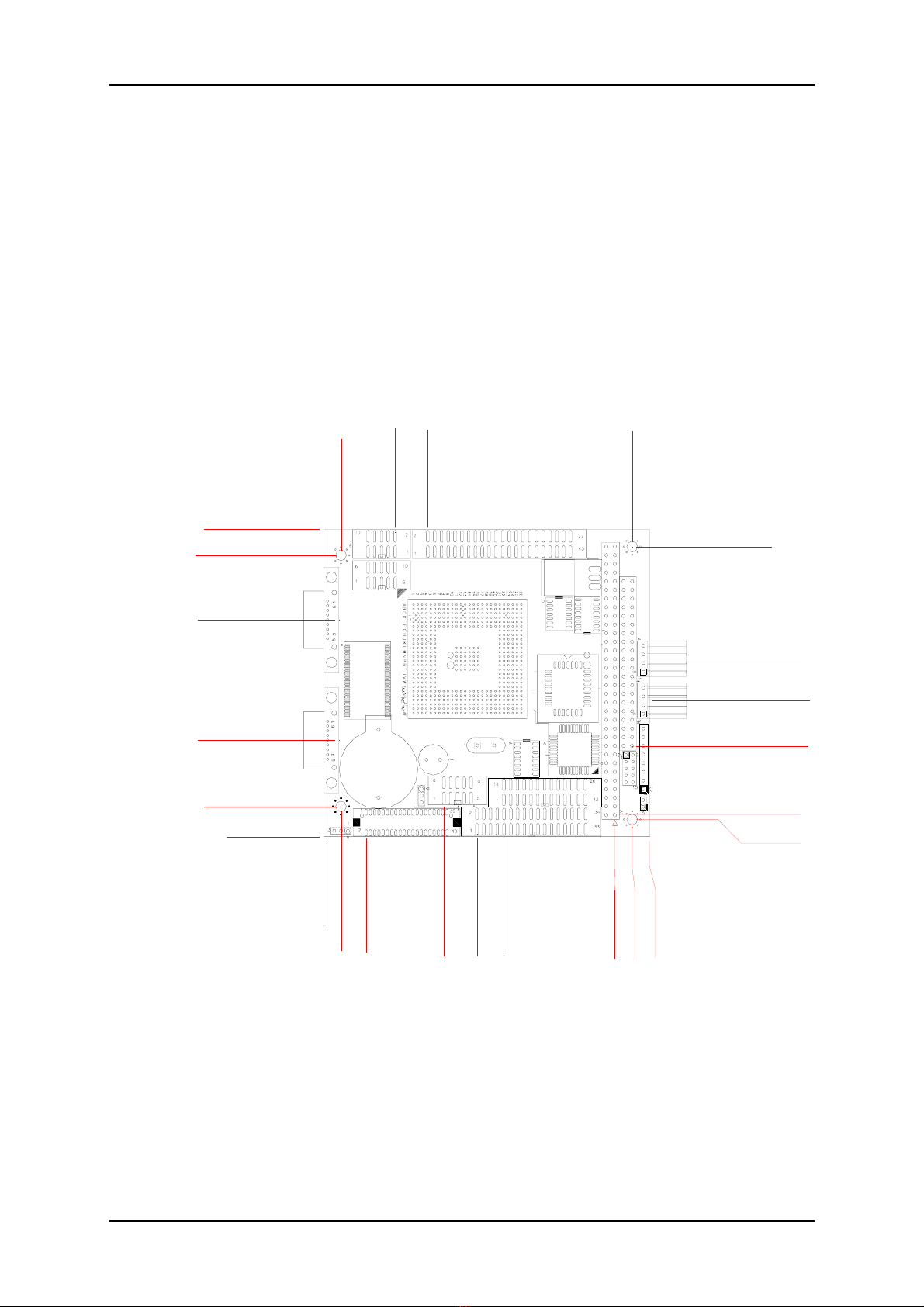
2.2 Connector Allocation ................................................................................................................. 2-2
Chapter 3 System Installation....................................................................................................3-1
3.1 Graphic Driver installation for STPC Atlas integrated GRAPHICS................................................. 3-1
3.2 IDE Interface................................................................................................................................ 3-1
3.3 SDRAM Interface........................................................................................................................ 3-1
3.4 Compact Flash interface ............................................................................................................ 3-2
3.5 Watch Dog Timer Programming .............................................................................................. 3-2
Chapter 4 BIOS Setup Information............................................................................................4-1
4.1 Entering Setup............................................................................................................................. 4-1
4.2 Main Menu .................................................................................................................................. 4-2
4.3 Standard CMOS Features Setup ............................................................................................... 4-3
4.4 IDE Adaptors Setup Menu ........................................................................................................ 4-4
4.5 Advanced BIOS Features Setup................................................................................................4-6
4.6 Advanced Chipset Features Setup ........................................................................................... 4-8
4.7 Integrated Peripherals.............................................................................................................. 4-10
4.8 Power Management Setup ......................................................................................................4-12
4.9 PnP/PCI Configuration Setup ................................................................................................ 4-14
4.10 Default Menu .......................................................................................................................... 4-16
4.11 Setup Password....................................................................................................................... 4-16
4.12 Exiting Seleting ....................................................................................................................... 4-17
4.13 POST Messages ....................................................................................................................... 4-17
4.14 BIOS POST Check Point List .................................................................................................4-22
4.15 Flash BIOS Utility ................................................................................................................... 4-28
Appendix A
Appendix B

Preface
How to Use This Manual
The manual describes how to configure your PEB-1431V system to meet various
operating requirements. It is divided into four chapters, with each chapter
addressing a basic concept and operation of Single Board Computer.
Chapter 1 : System Overview. Presents what you have in the box and give you an
overview of the product specifications and basic system architecture for this model
of single board computer.
Chapter 2 : Hardware Configuration. Shows the definitions and locations of
Jumpers and Connectors that you can easily configure your system.
Chapter 3 : System Installation. Describes how to properly mount the CPU, main
memory and CF flash disk to get a safe installation and provides a guide of Watch
Dog Timer function.
Chapter 4 : BIOS Setup Information. Specifies the meaning of each setup
parameters, how to get advanced BIOS performance and update new BIOS. In
addition, POST checkpoint list will give users some guidelines of trouble-shooting.
The content of this manual and EC declaration document is subject to change
without prior notice. These changes will be incorporated in new editions of the
document. Portwell may make supplement or change in the products described in
this document at any time.
Updates to this manual, technical clarification, and answers to frequently asked
questions will be shown on the following web site : http://www.portwell.com/.

System Overview
PEB-1431V User’s Manual 1-1
Chapter 1
System Overview
This manual describes in detail the Portwell PEB-1431V PC/104 Embedded System
Board. This manual aims to provide all necessary information to users who may
interest in using all PEB-1431V’s functions.
Please be aware that it is possible to create configurations within the CMOS RAM
that make booting impossible. If this should happen, clear the CMOS settings, (see
the description of the Jumper Settings for details).
We strongly recommend that you study this manual carefully before attempting to
alter PEB-1431V’s configurations. In the case, something in this manual is not clear
or users have any suggestion on this manual. Contact our Customer Service
department with the relevant details. Portwell Technical Service Group’s web site
is http://www.portwell.com/.
1.1 Introduction
The PEB-1431V is a compact PC/104 CPU Module that equips with STPC Atlas low-
power processor and integrated VGA.
This model is incredibly compact with flexible extension. There is a PC/104
interface, which is cable to add extra devices. For an embedded system, Watch Dog
Timer is also one standard feature. It helps to free the system from undesired
hanging without human interface. This is unique for many Embedded System
applications.
Other features include a built-in TFT LCD interface, a compact Flash socket for type
II Compact Flash storage card, two serial ports, one parallel port, and on board
16MB of SDRAM.

System Overview
PEB-1431V User’s Manual 1-2
1.2 Check List
The PEB-1431V package includes the following basic items accompany with this
manual.
1 PEB-1431V All-in-One STPC Atlas Computing Module
1 User’s Manual
1 CD-ROM contains the followings:
- VGA drivers and utilities
- Other driver and utilities (if have)
Cable set includes the followings:
- 1 PS/2 keyboard and mouse Y cable (10-pin, Mini-DIN)
- 1 IDE 2.5” HDD cable (44-pin, pitch 2.0mm, connect two IDE devices)
- 1 FDD cable (34-pin, pitch 2.0mm)
- 1 bracket with one Printer port cable (26-pin, pitch 2.0mm)
If any of these items is damaged or missed, please contact your vendor and save all
packing materials for future replacement and maintenance.
1.3 Product Specifications
Main processor
Onboard STPC Atlas 133MHz, BGA package
BIOS
AMI 256KB Flash BIOS
Chipset
STPC Atlas integrated
I/O chipset
Winbond W83977F-A
Memory
Onboard 16 Mbytes SDRAM
Enhanced IDE
Supports two IDE devices. Supports PIO mode 3 & 4 with data transfer rate up to
22MB/sec.
FDD interface
Supports up to two floppy disk drives, 5.25" (360KB and 1.2MB) and/or 3.5"
(720KB, 1.44MB, and 2.88MB)
Parallel port
Interface for bi-directional parallel port x 1. Supports SPP, ECP, and EPP modes

System Overview
PEB-1431V User’s Manual 1-3
Serial port
One external D-SUB 9 connector supports RS-232
One external D-SUB 9 connector supports RS-422/485
KB/Mouse connector
Internal header PS2 Keyboard/Mouse connector x 1
Watchdog timer
Support watchdog timer from 0.5 to 64 sec by hardware count & software trigger
DMA
7 DMA channels (8237 equivalent)
Interrupt
15 interrupt levels (8259 equivalent)
Power management
I/O peripheral devices support power saving and doze/standby/suspend modes
APM 1.2 compliant
Display chipset
STPC Atlas integrated
Display memory
Shared display memory up to 4MB
Display type
Supports interlaced or non-interlaced CRT
Support for VGA and SVGA active matrix TFT flat panels with 9,12,18-bit
interface
Resolution
Up to 1280x1024x75Hz CRT display
Programmable panel size up to 1024 by 1024 pixels
SSD interface
One CF socket supports Type II Compact Flash Card (Support 8-320MB Compact
flash)
Expansion interface
One 8-bit 104-pin connector onboard
Power connectors
4-pin FDD x 2

System Overview
PEB-1431V User’s Manual 1-4
1.3.1 Mechanical and Environmental
Power supply voltage: ±5V, ±12V
Typical power requirement: +5V @ 1.6A
Operating temperature: 32 to 131°F (0 to 55°C)
Board size: 96mm x 90mm
1.3.2 Mechanical Drawing
0
8.89
28.32
63.63
82.55
5.08
21.02
30.66
90.82
85.09
52.2
39.88
26.67
6.35
5.08
90.82
95.89
85.74
53.02
45.09
35.37
12.5
5.08
0
90.17

System Overview
PEB-1431V User’s Manual 1-5
1.4 System Architecture
1.4.1 TPC Atlas
The STPC Atlas system on chip provide the basic functionality and buses of the
system:
Interface to SDRAM, 64-bit data bus. PCI interface provided by STPC Atlas.
VGA controller with video memory shared with system memory (UMA).
IDE interface support Ultra DMA. Tow connectors are provided: A 44 pin pitch
2.0mm standard IDE interface on the primary controller and a Compact Flash
connector on the secondary controller.
1.4.2 STPC Atlas Integrated Graphics
The STPC Atlas integrated Graphics is very cost efficient since almost no additional
components are required. This is achieved by using the SDRAM as frame-buffer and
by integrating the graphics engine. It provides both CRT and Panel display
interfaces.
1.4.3 PC/104 Interface
The STPC Atlas system on chip provides an ISA Bus that may operate in master or
slave mode. The bus master has the ability to generate bus cycles and thereby
transfer data without involvement of the CPU or DMA (Direct memory access). A
104-pin PC/104 connector is equipped onboard for future expansion.
1.4.4 SDRAM Interface
This on board 16 MB SDRAM are recommended to use.
1.4.5 IDE Interface
A primary as well as a secondary IDE controller is provided by the STPC Atlas
which supports Ultra DMA mode and PCI bus mastering for the data transfer.
Access to these controllers is provided by a standard IDE 44-pin connector and a
Compact Flash type II connector on the solder side of this board.

System Overview
PEB-1431V User’s Manual 1-6
1.4.6 STPC Atlas and Winbond W83977F-A
The STPC Atlas integrated Super I/O chip provides most input / output interfaces
of the system as the following:
COM 1. A RS-232 driver is used whereby RS-232 are provided. Driver uses charge
pumps whereby only +5V is required
COM 2. A RS-422/485 driver is used whereby RS-422/485 are provided.
Selection of the mode is made by hardware jumper
LPT. Support for SPP, EPP and ECP modes
Floppy interface
Keyboard interface
PS/2 Mouse interface
Provision of buffered ISA data bus for BIOS
NVRAM with battery backup for BIOS configuration and real time clock
1.4.7 Compact Flash Interface
A Compact Flash type II connector is connected to the secondary IDE controller. The
Compact Flash storage card is IDE compatible. It is an ideal replacement for
standard IDE hard drives. The solid-state design offers no seek errors even under
extreme shock and vibration conditions. The Compact Flash storage card is
extremely small and highly suitable for rugged environments, thus providing an
excellent solution for mobile applications with space limitations. It is fully
compatible with all consumer applications designed for data storage PC card, PDA,
and Smart Cellular Phones, allowing simple use for the end user. The Compact Flash
storage card is O/S independent, thus offering an optimal solution for embedded
systems operating in non-standard computing environments. The Compact Flash
storage card is IDE compatible and offers various capacities.
The following block diagram shows the architecture and main components of PEB-
1431V.

System Overview
PEB-1431V User’s Manual 1-7
MEMORY (16MB Onboard)
STPC
Atlas
(516BGA)
ISA BUS
BIOS
Super I/O
W83977F-A
(128 PQFD)
Parallel Port
Floppy
TFT
Serial Port
COM 1/2
VGA EIDE
USB (Optional)
PS/2 Keyboard
Mouse
Figure 1-1 PEB-1431V System Block Diagram
The two key components on board are the STPC Atlas and the Windbond Super I/O
chip. These two devices provide the ISA and PCI bus to which all the major
components are attached.

Hardware Configuration
PEB-1431V User’s Manual 2-1
Chapter 2
Hardware Configuration
This chapter indicates jumpers’, headers’ and connectors’ location. Users may find
useful information related to hardware settings in this chapter. The default settings
are indicated with a star sign (Ì).
2.1 Jumper Setting
The jumper settings are used to select options for different features. The adjustment
made aims to let users customize PEB-1431V’s features. In the following sections,
short means covering a jumper cap over jumper pins; open or NC (Not Connected)
means removing a jumper cap from jumper pins.
Figure 2-1 Jumper Location Diagram
JP1: Watch Dog Time Function
JP1 Function
1-2 Short Disable WDT FunctionÌ
1-2 Open Enable WDT Function
3-4 Short Allocate I/O port 543/343
3-4 Open Allocate I/O port 533/033Ì
JP3
1

Hardware Configuration
PEB-1431V User’s Manual 2-2
5-6 7-8 9-10 Time-out Interval
Short Short Short 0.5 Sec
Short Short NC 1 SecÌ
Short NC Short 2 Sec
Short NC NC 4 Sec
NC Short Short 8 Sec
NC Short NC 16 Sec
NC NC Short 32 Sec
NC NC NC 64 Sec
JP2: CMOS Clear
JP2 Function
1-2 Short Normal Ì
2-3 Short Clear CMOS
JP3: COM2 RS-422/485 Selection Jumper
JP3 Function
1-2 Short COM2 RS-422Enable Ì
2-3 Short COM2 RS-485Enable
2.2 Connector Allocation
Figure 2-2 Connector Location Diagram

Hardware Configuration
PEB-1431V User’s Manual 2-3
Connector’s Function List
Connector Location Description
J1 Two USB Connector
J2 PS/2 Keyboard& Mouse connector
J3 IDE Interface Connector
J4 D-SUB 9 pin connector (COM1)
J5 +5V, +12V Power Connector
J6 -5V, -12V power connector
J7 D-SUB 9 pin connector (COM2)
J8 VGA Connector
J9 Parallel Port Connector
J10 CPLD 8-pin connector
J11 TFT LCD Panel Connector
J12 Floppy disk interface
J13 Reset Header
J14 Compact Flash Socket
Pin Assignments of Connectors
J1: Two-port USB Interface Connector (2 x 5 shrouded header)
PIN No. Signal Description PIN No. Signal Description
1 +5V 2 GND
3 USBD0- 4 GND
5 USBD0+ 6 USBD1+
7 GND 8 USBD1+
9 GND 10 +5V
J2: PS/2 Keyboard/Mouse Connector (2 x 5 shrouded header)
PIN No. Signal Description
1 Mouse Data
2 NC
3 GND
4 +5V
5 Mouse Clock
6 Keyboard Data
7 NC
8 GND
9 +5V
10 Keyboard Clock

Hardware Configuration
PEB-1431V User’s Manual 2-4
J3: IDE Interface Connector (44 pin)
PIN No. Signal Description PIN No. Signal Description
1 RESET# 2 Ground
3 Data 7 4 Data 8
5 Data 6 6 Data 9
7 Data 5 8 Data 10
9 Data 4 10 Data 11
11 Data 3 12 Data 12
13 Data 2 14 Data 13
15 Data 1 16 Data 14
17 Data 0 18 Data 15
19 Ground 20 N/C
21 DMA REQ 22 Ground
23 IOW# 24 Ground
25 IOR# 26 Ground
27 IOCHRDY 28 Pull-down
29 DMA ACK# 30 Ground
31 INT REQ 32 N/C
33 SA1 34 CBLID#
35 SA0 36 SA2
37 HDC CS0# 38 HDC CS1#
39 HDD Active# 40 Ground
41 +5V 42 +5V
43 Ground 44 Ground
J4: Serial Port-1 D-SUB 9 pin Connector
PIN No. Signal Description
1 Data Carrier Detect (DCD)
2 ReceiveData(RXD)
3 Transmit Data (TXD)
4 Data Terminal Ready (DTR)
5 Ground(GND)
6 Data Set Ready (DSR)
7 RequesttoSend(RTS)
8 Clear to Send (CTS)
9 Ring Indicator (RI)

Hardware Configuration
PEB-1431V User’s Manual 2-5
J5: +5V, +12V Power Connector
PIN No. Signal Description
1 +12V
2 GND
3 GND
4 +5V
J6: -5V, -12V Power Connector
PIN No. Signal Description
1 -12V
2 GND
3 GND
4 -5V
J7: Serial Port-2 D-SUB 9 pin Connector
PIN No. Signal Description
1 RS-422 TX- / RS-485 TX-
2 RS-422 RX+
3 RS-422 TX+/ RS-485 TX+
4 RS-422 RX-
5 Ground(GND)
6 N/C
7 N/C
8 N/C
9 N/C
J8: VGA Connector (2 x 5 shrouded header)
PIN No. Signal Description
1 R
2 G
3 B
4 VSYNC
5 HSYNC
6 VGA_I2CSCL
7 Ground
8 VGA_I2CSDA
9 Ground
10 N/C

Hardware Configuration
PEB-1431V User’s Manual 2-6
J9: Parallel Port Connector
PIN No. Signal Description PIN No. Signal Description
1 Strobe# 14 Auto Form Feed#
2 Data 0 15 Error#
3 Data 1 16 Initialization#
4 Data 2 17 Printer Select IN#
5 Data 3 18 Ground
6 Data 4 19 Ground
7 Data 5 20 Ground
8 Data 6 21 Ground
9 Data 7 22 Ground
10 Acknowledge# 23 Ground
11 Busy 24 Ground
12 Paper Empty 25 Ground
13 Printer Select 26 N/C
J10: CPLD 8-pin Connector
PIN No. Signal Description
1 +5V
2 TDO
3 TDI
4 N/C
5 N/C
6 TMS
7 Ground
8 TCK
J11: TFT LCD Connector
PIN No. Signal Description PIN No. Signal Description
1 GND 2 GND
3 R0 4 R1
5 R2 6 R3
7 R4 8 R5
9 GND 10 GND
11 G0 12 G1
13 G2 14 G3
15 G4 16 G5
17 GND 18 GND
19 B0 20 B1
21 B2 22 B3

Hardware Configuration
PEB-1431V User’s Manual 2-7
23 B4 24 B5
25 GND 26 GND
27 FPLINE 28 FPFRAME
29 DE 30 DCLK
31 N/C 32 N/C
33 TFT PWM 34 N/C
35 VCC 36 +12V
37 VCC 38 +12V
39 TFT_ENVCC 40 TFT_ENVDD
J12: FDC Interface Connector
PIN No. Signal Description PIN No. Signal Description
1 Ground 2 Density Select 0
3 Ground 4 N/C
5 Ground 6 Density Select 1
7 Ground 8 Index#
9 Ground 10 Motor ENA#
11 Ground 12 Drive Select B#
13 Ground 14 Drive Select A#
15 Ground 16 Motor ENB#
17 Ground 18 Direction#
19 Ground 20 Step#
21 Ground 22 Write Data#
23 Ground 24 Write Gate#
25 Ground 26 Track 0#
27 Ground 28 Write Protect#
29 Ground 30 Read Data#
31 Ground 32 Head Select#
33 Ground 34 Disk Change#
J13: Reset Header
PIN No. Signal Description
1 RESET
2 GND

System Installation
PEB-1431V User’s Manual 3-1
Chapter 3
System Installation
This chapter provides you with instructions on how to set up your computer system
using PEB-1431V Embedded System Board. The additional information shows you
how to install graphic in Operating System.
3.1 Graphic Driver installation for STPC Atlas integrated GRAPHICS
The STPC Atlas integrated Graphics is very cost efficient since almost no additional
components are required. This is achieved by using the SDRAM as frame-buffer and
by integrating the graphics engine and display interface. This controller provides
both CRT and Panel display interfaces.
Driver Support
PEB-1431V provides one CD-Title to support on-board VGA device drivers in
various operating systems. Before installing the device driver, please see the
reference files in each sub-directory. If you have problems to install drivers directly
from CDROM, please copy the files into your hard drive before you proceed with
the driver installation.
VGA: This driver supports Windows-4.0, Windows-9X, Linux and QNX.
3.2 IDE Interface
A primary IDE controller is provided by the STPC Atlas system on chip, which
supports Ultra DMA mode and PCI bus mastering for the data transfer.
Access to these controllers is provided by a standard IDC 44-pin connector and a
Compact Flash type II connector on the solder side of this board.
3.3 SDRAM Interface
This board 16MB SDRAM are recommended to use.

System Installation
PEB-1431V User’s Manual 3-2
3.4 Compact Flash interface
A Compact Flash type II connector is connected to the secondary IDE controller. The
Compact Flash storage card is IDE compatible. It is an ideal replacement for
standard IDE hard drives. The solid-state design offers no seek errors even under
extreme shock and vibration conditions. The Compact Flash storage card is
extremely small and highly suitable for rugged environments, thus providing an
excellent solution for mobile applications with space limitations. It is fully
compatible with all consumer applications designed for data storage PC card, PDA,
and Smart Cellular Phones, allowing simple use for the end user. The Compact Flash
storage card is O/S independent, thus offering an optimal solution for embedded
systems operating in non-standard computing environments. The Compact Flash
storage card is IDE compatible and offers various capacities.
3.5 Watch Dog Timer Programming
There are one manners to activate the Watch-Dog Timer (WDT) function. You can
utilize hardware jumper setting and programmed by software command. After this
feature is enabled, a system reset will be generated unless an application triggers the
timer periodically within time-out period. This allows the system to restart in an
orderly way in case of any abnormal condition is found.
This WDT comes with 8 possible ranges of time intervals from 0.5 s to 64 sec., which
can be adjusted by setting jumper positions. It could be enabled and programmed by
reading I/O port 0533H or 0543H to issue trigger continuously, and disabled by
reading I/O port 0033H or 0343H. A tolerance of 30% timer limit must be
considered. For instance, if the time-out interval is set to 1second, the WDT trigger
command must be issued within 700ms at least.
The below example gives you a reference algorithm for WDT programming via I/O
port 0533H and 0033H in your application program:
Enable WDT
MOV DX, 0533H
IN AL, DX
Re-trigger WDT
MOV DX, 0533H
IN AL, DX
Disable WDT
MOV DX, 0033H
IN AL, DX
Table of contents
Other Portwell Industrial PC manuals
Popular Industrial PC manuals by other brands

Psion Teklogix
Psion Teklogix 8525 user manual

Neousys Technology
Neousys Technology SEMIL-1300GC Series user manual

Aplex
Aplex NV-266 C Series user manual

Bartec
Bartec Agile S Series Faq

AXIOMTEK
AXIOMTEK tBOX322-882-FL Quick installation guide

Neousys Technology
Neousys Technology SEMIL-1700GC Series Quick installation guide

Digital Electronics Corporation
Digital Electronics Corporation PL-3900T Series installation guide

Moxa Technologies
Moxa Technologies IA241-LX Quick installation guide

KEBCO
KEBCO C6 P34 BOX Series Instructions for use

Pro-face
Pro-face PL-B910 Series user manual

Delta
Delta DIAVH-PPC153100 user manual

JHCTech
JHCTech KMDA-3601 user manual