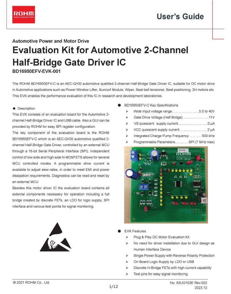
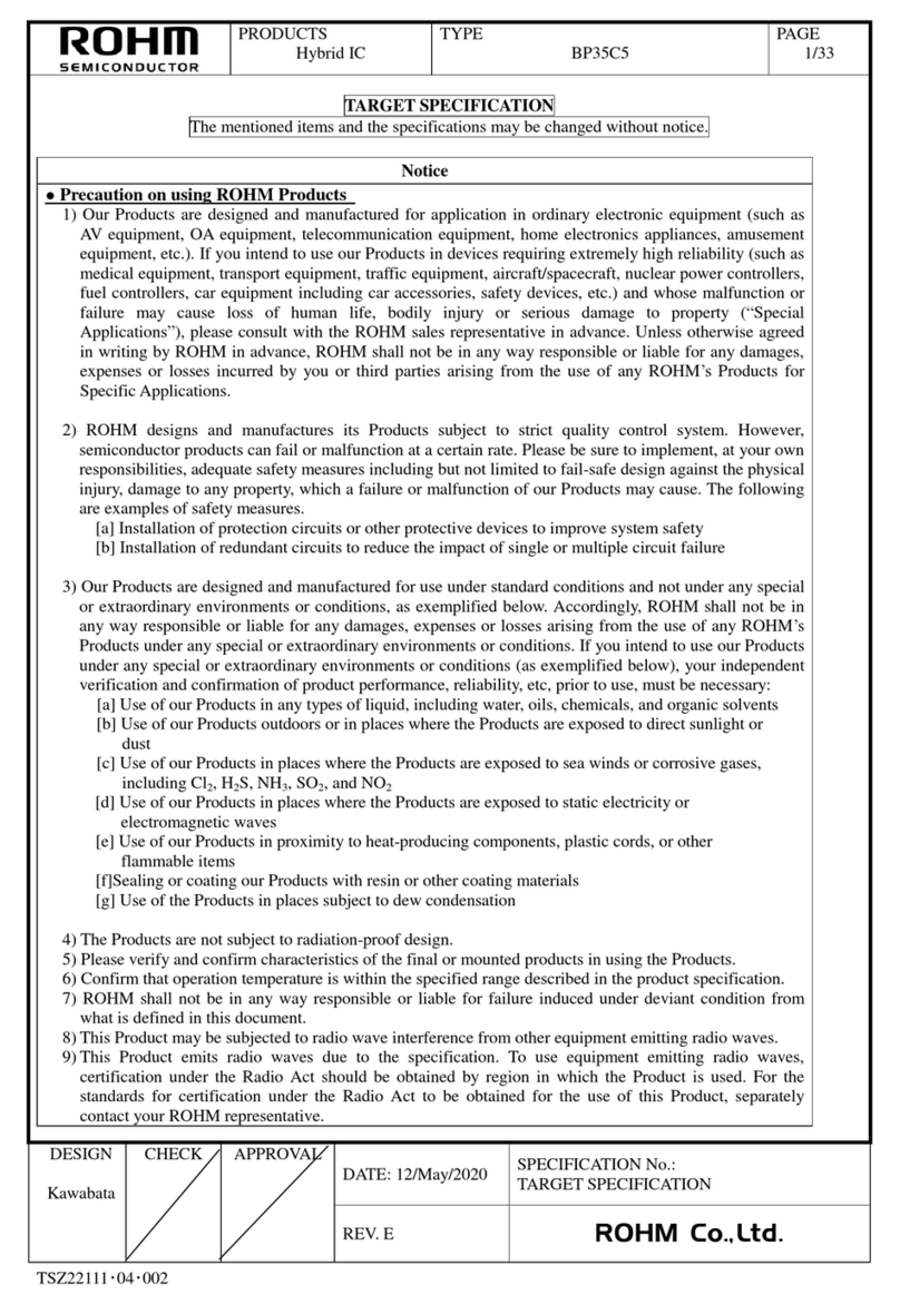
Rohm BD9P208MUF-TSB-001 User manual

© 2022 ROHM Co., Ltd.
66UG052E Rev.001
Jul.2023
User’s Guide
Primary Buck DC/DC Converter
Single 2.2 MHz Buck DC/DC Converter
For Automotive
BD9P208MUF-C Evaluation Board
BD9P208MUF-TSB-001 (3.5 to 40V Input, 2.0A)
Introduction
This user’s guide will provide the necessary steps to operate the Evaluation Board of ROHM’s BD9P208MUF-C Buck DC/DC
converter. This includes the external parts, operating procedures and application data.
Description
This Evaluation Board was developed for ROHM’s single 2.2 MHz buck DC/DC converter BD9P208MUF-C. BD9P208MUF-
C is a current mode synchronous buck DC/DC converter with integrated POWER MOSFETs. The BD9P208MUF-C accepts a
power supply input range of 3.5 V to 40 V and generates a maximum output current of 2 A. BD9P208MUF-C generates an
output voltage range of 0.8 V to 8.5 V using external resistors.
Application
Automotive Powered Supplies
Consumer Powered Supplies
Recommended Operating Conditions
Table 1. Recommended Operating Conditions
Parameter
Min
Typ
Max
Units
Conditions
Input Voltage
3.5
-
40
V
Initial startup is 4.0 V or more
Output Voltage (Note1)
0.8
-
8.5
V
Output Current Range
-
-
2.0
A
OCP_SEL = H : 1.5 A (Max)
OCP_SEL = L : 2.0 A (Max)
Switching Frequency
-
2.2
-
MHz
Maximum Efficiency
-
86.1
-
%
VO = 3.3 V, Io = 0.8 A, Ta = 25 °C
Maximum Efficiency
-
91.3
-
%
VO = 5.0 V, Io = 1.1 A, Ta = 25 °C
(Note1) Although the minimum output voltage is configurable up to 0.8 V, it may be limited by the SW min ON pulse width. For
the same reason, although the maximum output voltage is configurable up to 8.5 V, it may be limited by the SW minimum OFF
pulse width.

2/8
© 2022 ROHM Co., Ltd.
66UG052E Rev.001
Jul.2023
User’s Guide
BD9P208MUF-C
Evaluation Board
Figure 1. Evaluation Board Top View
Evaluation Board Schematic
Figure 2. Circuit Diagram
Operating Procedure
1. Turn off EN and connect the GND terminal of the power supply to the GND terminal of Evaluation Board.
2. Connect VCC pin of power supply to the VBAT pin of the Evaluation Board.
3. Connect the load to the Evaluation Board’s VOUT and GND terminals. When using an electronic load, connect with the
load turned off.
4. Connect a voltmeter to the Evaluation Board's VOUT and GND terminals.
5. Turn on the Power supply of VBAT. Turn ON the switch of EN terminal.
6. Make sure that the voltmeter is set to measure voltage.
7. Turn on the electronic load.
(Caution) This Evaluation Board does not support hot plug. Do not perform hot plug test.
(Note) If EN = High (EN short to VIN) before Power ON, the turn ON and turn OFF is controlled by VBAT only.

3/8
© 2022 ROHM Co., Ltd.
66UG052E Rev.001
Jul.2023
User’s Guide
BD9P208MUF-C
Operation Mode Settings
Below is a table of BD9P208MUF-C operation modes selectable using OCP_SEL, MODE and SSCG terminals.
Table 2. Mode Settings
Terminal
Setting
Operation Mode
Function
OCP_SEL
HIGH
OCP threshold selection
OCP threshold is set to 2.250 A (Typ.)
Output Current maximum is 1.5 A.
LOW
OCP threshold is set to 3.0 A (Typ.)
Output Current maximum is 2.0 A.
MODE
HIGH
FPWM
Forced PWM mode
LOW or OPEN
AUTO
Automatically switched between PWM
and LLM mode.
Apply a clock to this pin
SYNC
Activate synchronization mode
SSCG
ON (HIGH)
Select Spread Spectrum
function
Enable Spread Spectrum
OFF (LOW)
Disable Spread Spectrum
(Note) If setting is High, the terminal is shorted to VREG, and if setting is Low, the terminal is shorted to GND.

4/8
© 2022 ROHM Co., Ltd.
66UG052E Rev.001
Jul.2023
User’s Guide
BD9P208MUF-C
Pin Configuration
Figure 3. Pin Configuration (Top View)
Parts List (BD9P208MUF-C)
Table 3. Parts list (3.3 V, 2.0 A)
Part No
Value
PKG(inch)
PKG(mm)
Manufacturer
Part Name(Series)
π type filter
CF1
4.7μF
1210
3225
Murata
GCM32ER71H475K
CF3
Open
-
-
-
-
LF1
2.2μH
2524h18
6360h45
TDK
CLF6045NIT-2R2N-D
CF2
0.1μF
0402
1005
Murata
GCM155R71H104K
CBLK
220μF
0404h04
1010h10
Nichicon
UWD1V221MCL1GS
Basic
CIN2
4.7μF
1210
3225
Murata
GCM32ER71H475K
CIN1
0.1μF
0402
1005
Murata
GCM155R71H104K
CIN1B
Open
-
-
-
-
CVREG
1μF
0805
2012
Murata
GCM21BR71C105K
CBST
0.1μF
0402
1005
Murata
GCM155R71H104K
RBST
0Ω
0402
1005
ROHM
MCR01 Series
RSNB
Open
-
-
-
-
CSNB
Open
-
-
-
-
RRST
10kΩ
0402
1005
ROHM
MCR01 Series
RRST2 (Note 3)
Open
-
-
-
-
Application
L1
3.3μH
2524h18
6360h45
TDK
CLF6045NIT-3R3N-D
COUT1 (Note 1)
22μF
1210
3225
Murata
GCM32ER71A226K
COUT2 (Note 1)
22μF
1210
3225
Murata
GCM32ER71A226K
COUT3 (Note 1)
Open
-
-
-
-
COUT4 (Note 1)
Open
-
-
-
-
RFB0
0Ω
0402
1005
ROHM
MCR01 Series
RFB1
75kΩ
0402
1005
ROHM
MCR01 Series
RFB2
24kΩ
0402
1005
ROHM
MCR01 Series
CFB1 (Note 4)
Open
-
-
-
-
CFB2 (Note 4)
Open
-
-
-
-
RDIS
0Ω
0402
1005
ROHM
MCR01 Series
RDISN
Open
-
-
-
-
REX (Note 2)
0Ω
0402
1005
ROHM
MCR01 Series
REXN (Note 2)
Open
-
-
-
-

5/8
© 2022 ROHM Co., Ltd.
66UG052E Rev.001
Jul.2023
User’s Guide
BD9P208MUF-C
Table 4. Parts list (5.0 V, 2.0 A)
Part No
Value
PKG(inch)
PKG(mm)
Manufacturer
Part Name(Series)
π type filter
CF1
4.7μF
1210
3225
Murata
GCM32ER71H475K
CF3
Open
-
-
-
-
LF1
2.2μH
2524h18
6360h45
TDK
CLF6045NIT-2R2N-D
CF2
0.1μF
0402
1005
Murata
GCM155R71H104K
CBLK
220μF
0404h04
1010h10
Nichicon
UWD1V221MCL1GS
Basic
CIN2
4.7μF
1210
3225
Murata
GCM32ER71H475K
CIN1
0.1μF
0402
1005
Murata
GCM155R71H104K
CIN1B
Open
-
-
-
-
CVREG
1μF
0805
2012
Murata
GCM21BR71C105K
CBST
0.1μF
0402
1005
Murata
GCM155R71H104K
RBST
0Ω
0402
1005
ROHM
MCR01 Series
RSNB
Open
-
-
-
-
CSNB
Open
-
-
-
-
RRST
10kΩ
0402
1005
ROHM
MCR01 Series
RRST2 (Note 3)
Open
-
-
-
-
Application
L1
3.3μH
2524h18
6360h45
TDK
CLF6045NIT-3R3N-D
COUT1 (Note 1)
22μF
1210
3225
Murata
GCM32ER71A226K
COUT2 (Note 1)
22μF
1210
3225
Murata
GCM32ER71A226K
COUT3 (Note 1)
Open
-
-
-
-
COUT4 (Note 1)
Open
-
-
-
-
RFB0
0Ω
0402
1005
ROHM
MCR01 Series
RFB1
68kΩ
0402
1005
ROHM
MCR01 Series
RFB2
13kΩ
0402
1005
ROHM
MCR01 Series
CFB1 (Note 4)
Open
-
-
-
-
CFB2 (Note 4)
Open
-
-
-
-
RDIS
0Ω
0402
1005
ROHM
MCR01 Series
RDISN
Open
-
-
-
-
REX (Note 2)
0Ω
0402
1005
ROHM
MCR01 Series
REXN (Note 2)
Open
-
-
-
-
(Note 1)
Max
Output
Current
VOUT
OCP_SEL
Recommended L
Value
Recommended COUT
Value
Minimum COUT Value
(Note1-1,2)
2.0 A
≥ 3.3 V
L
3.3 μH
COUT ≥ 44 μF
COUT_WORST ≥ 30 μF
> 1.1 V
< 3.3 V
3.3 μH
COUT ≥ 145.2
𝑉𝑂𝑈𝑇 μF (*)
COUT_WORST ≥ 99.0
𝑉𝑂𝑈𝑇 μF (*)
≤ 1.1 V
4.7 μH
COUT ≥ 217.8
𝑉𝑂𝑈𝑇 μF (*)
COUT_WORST ≥ 148.5
𝑉𝑂𝑈𝑇 μF (*)
1.5 A
≥ 3.3 V
H
4.7 μH
COUT ≥ 32 μF
COUT_WORST ≥ 20 μF
> 1.1 V
< 3.3 V
4.7 μH
COUT ≥ 105.6
𝑉𝑂𝑈𝑇 μF (*)
COUT_WORST ≥ 66.0
𝑉𝑂𝑈𝑇 μF (*)
≤ 1.1 V
6.8 μH
COUT ≥ 126.7
𝑉𝑂𝑈𝑇 μF (*)
COUT_WORST ≥ 100.0
𝑉𝑂𝑈𝑇 μF (*)
* VOUT is the output voltage [V]
(Note 1-1) When selecting the output capacitor, ensure that the capacitance, COUT_WORST, of the above equation is maintained
at the characteristics of DC Bias, AC Voltage, temperature, and tolerance.
(Note 1-2) If the capacitance falls below this value, oscillation may happen. When using electrolytic capacitor and conductive
polymer hybrid aluminum electrolytic capacitor, please place it in addition to the ceramic capacitors with the capacity described
above. The changes in the frequency characteristic are greatly affected by the type and the condition (temperature, etc.) of parts
that are used, the wire routing and the layout of the PCB. Please confirm stability and responsiveness in actual application.

6/8
© 2022 ROHM Co., Ltd.
66UG052E Rev.001
Jul.2023
User’s Guide
BD9P208MUF-C
(Note 2) VCC_EX is power supply input for internal circuit. VREG voltage is supplied from VCC_EX when voltage between 3.2V
(VTEXH, Max) and 5.65 V (VEXOVPL, Min) is connected to this pin. Connecting this pin to VOUT improves efficiency. In case of
not use this function, connect this pin to GND.
Output Voltage
REX setting
REXN setting
VCC_EX State
3.2 V ≤ VOUT ≤ 5.65 V
0 Ω
Open
Connected to VOUT
VOUT < 3.2 V or
VOUT > 5.65 V
Open
0 Ω
Connected to GND
(Note 3) RESET terminal should be pulled-up to VREG via RRST2 when the output setting is over 6.5 V because RESET pin’s
absolute maximum rating is 7.0 V. If RESET is not pulled-up to VOUT, it can be pulled-up to VREG via RRST2 by default.
(Note 4) Please use CFB1 and CFB2 PCB patterns to improve the frequency characteristics. Set these values by following
the guide in page 31 of datasheet.
(Note 5) If the recommended parts on tables 3 to 7 are not available anymore due to end of production, different parts will be
used on the test board because the end of production parts are deprecated.

7/8
© 2022 ROHM Co., Ltd.
66UG052E Rev.001
Jul.2023
User’s Guide
BD9P208MUF-C
Board Layout
Evaluation Board PCB information
Number of Layers
Material
Board Size
Copper Thickness
4
FR-4 High Tg
100mm x 75mm x 1.6mm
2oz(70μm) / 1oz (35μm) / 1oz (35μm) / 2oz(70μm)
The layout is shown below.
Figure 4. Top Layer Layout
(Top View)
Figure 5. Middle1 Layer Layout
(Top View)
Figure 6. Middle2 Layer Layout
(Top View)
Figure 7. Bottom Layer Layout
(Top View)

8/8
© 2022 ROHM Co., Ltd.
66UG052E Rev.001
Jul.2023
User’s Guide
BD9P208MUF-C
Revision History
Date
Revision
Number
Description
7. Jul. 2023
001
New release

www.rohm.com
Notice
ROHM Customer Support System
R2043A
The information contained in this document is intended to introduce ROHM Group (hereafter
referred to asROHM) products. When using ROHM products, please verify the latest specifications
or datasheets before use.
ROHM products are designed and manufactured for use in general electronic equipment and
applications (such as Audio Visual equipment, Office Automation equipment, telecommunication
equipment, home appliances, amusement devices, etc.) or specified in the datasheets. Therefore,
please contact the ROHM sales representative before using ROHM products in equipment or
devices requiring extremely high reliability and whose failure or malfunction may cause danger or
injury to human life or body or other serious damage (such as medical equipment, transportation,
traffic, aircraft, spacecraft, nuclear power controllers, fuel control, automotive equipment including
car accessories, etc. hereafter referred to as Specific Applications). Unless otherwise agreed in
writing by ROHM in advance, ROHM shall not be in any way responsible or liable for any damages,
expenses, or losses incurred by you or third parties arising from the use of ROHM Products for
Specific Applications.
Electronic components, including semiconductors, can fail or malfunction at a certain rate. Please
be sure to implement, at your own responsibilities, adequate safety measures including but not
limited to fail-safe design against physical injury, and damage to any property, which a failure or
malfunction of products may cause.
The information contained in this document, including application circuit examples and their
constants, is intended to explain the standard operation and usage of ROHM products, and is not
intended to guarantee, either explicitly or implicitly, the operation of the product in the actual
equipment it will be used. As a result, you are solely responsible for it, and you must exercise your
own independent verification and judgment in the use of such information contained in this
document. ROHM shall not be in any way responsible or liable for any damages, expenses, or
losses incurred by you or third parties arising from the use of such information.
When exporting ROHM products or technologies described in this document to other countries, you
must abide by the procedures and provisions stipulated in all applicable export laws and regulations,
such as the Foreign Exchange and Foreign Trade Act and the US Export Administration
Regulations, and follow the necessary procedures in accordance with these provisions.
The technical information and data described in this document, including typical application circuits,
are examples only and are not intended to guarantee to be free from infringement of third parties
intellectual property or other rights. ROHM does not grant any license, express or implied, to
implement, use, or exploit any intellectual property or other rights owned or controlled by ROHM or
any third parties with respect to the information contained herein.
No part of this document may be reprinted or reproduced in any form by any means without the
prior written consent of ROHM.
All information contained in this document is current as of the date of publication and subject to
change without notice. Before purchasing or using ROHM products, please confirm the latest
information with the ROHM sales representative.
ROHM does not warrant that the information contained herein is error-free. ROHM shall not be in
any way responsible or liable for any damages, expenses, or losses incurred by you or third parties
resulting from errors contained in this document.
Thank you for your accessing to ROHM product informations.
More detail product informations and catalogs are available, please contact us.
Notice
© 2023 ROHM Co., Ltd. All rights reserved.
https://www.rohm.com/contactus
1)
2)
3)
4)
5)
6)
7)
8)
9)
Table of contents
Other Rohm Computer Hardware manuals

Rohm
Rohm BD9P108MUF-TSB-001 User manual

Rohm
Rohm PMIC BD96801 User manual

Rohm
Rohm BU1570KN Specification sheet

Rohm
Rohm BP35C5 User manual

Rohm
Rohm BD16950EFV-EVK-001 User manual

Rohm
Rohm LAPIS Semiconductor ML62Q1739 User manual

Rohm
Rohm LAPIS Semiconductor ML22660 User manual

Rohm
Rohm LAPIS Semiconductor ML7404 Series Guide

Rohm
Rohm BD71805MWV Guide

Rohm
Rohm BD7682FJ-EVK-301 User manual