Sharp ER-A220 User manual

ELECTRONIC
CASH REGISTER
MODEL ER-A220
(For"V"version)
SRV Key:LKGIM7113RCZZ
PRINTER:LTP-1245
CAUTION
EXTREMECAUTIONMUSTBETAKEN WHEN SERVICINGTHISMACHINE. EVENTHOUGH
THEMODESWITCH IS INTHE OFF POSITION,VOLTAGE IS STILL SUPPLIEDTO THEEN-
TIREMACHINE.
WHEN WORKING ON THIS MACHINE MAKE SURE THAT THE POWER CORDIS REMOVED
FROMTHEWALLOUTLET.
CHAPTER 1. SPECIFICATIONS.................................................................1 - 1
CHAPTER 2. OPTIONS...............................................................................2 - 1
CHAPTER 3. SERVICE (SRV) MODE.........................................................3 - 1
CHAPTER 4. HARDWARE DESCRIPTION ................................................4 - 1
CHAPTER 5. TEST FUNCTION ..................................................................5 - 1
CHAPTER 6. DOWN LOAD FUNCTION.....................................................6 - 1
CHAPTER 7. SERVICE PRECAUTION.......................................................7 - 1
CHAPTER 8. IPL (Initial Program Loading) FUNCTION .............................8 - 1
CHAPTER 9. INSTALLATION OF OPTIONS..............................................9 - 1
CHAPTER 10. CIRCUIT DIAGRAM & PWB LAYOUT ...............................10 - 1
PARTS GUIDE
CONTENTS
Parts marked with " " is important for maintaining the safety of the set. Be sure to replace these parts with specified
ones for maintaining the safety and performance of the set.
SHARP CORPORATION This document has been published to be used
for after sales service only.
The contents are subject to change without notice.
SERVICE MANUAL

CHAPTER 1. SPECIFICATIONS
1. Appearance/Rating
1) Rating
Power source AC local voltage( 10%), 50/60Hz
Power consumption Max. 45W, Stand-by : 20W
Operating temperature 0°C~40°C
Operating humidity 10%~90%
Physical dimensions,
including the drawer 330(W) x 363(D) x 238(H)mm
Weight 8.9 kg
2. Keyboard
1) Standard keyboard layout (15 Departments)
Fig. 2-1
2) Option keyboard layout
There are following Department keylayout selections by PGM pro-
gramming (JOB#61-A)
3) Key top name
Standard Key Top
KEY TOP DESCRIPTION
0 to 9,00 Numeric keys
Decimal point key
CL Clear key
Multiplication key
1 to 15 Department 1 to 15 keys
Paper feed key
CASH # Cashier code entry key
RA Received on Account key
Void key
AUTO 1, 2 Automatically Entry key 1, 2
EX Currency conversion key
PLU PLU/Subdept code entry key
AMT Amount Entry key
%1, 2 % key 1, 2
(–) Discount key
SHIFT Department shift key for DEPT. 16 – 30 key
CH Check key
CR Credit key
TL/NS Total and No sale key
RCPT/PO After receipt issue & Paid out key
RF Refund key
#/TM/ST Non-add code entry, Time display and Tax
included subtotal key
Optional Key Top
KEY TOP DESCRIPTION
16-30 Department key 16-30
3. Mode switch
Fig. 3-1
The key can be removed in the REG or position.
In the SRV’ mode, key inputs are prohibited and no display is made.
With the key in the off position power is not supplied to the main
PWB.
000
123
11
12
456
789
13
14
15
WYPL2
WYPL2
WYPL2
AMTPLU
CL
ESC
SHIFT
AUTO
2
AUTO
1
%1 %2
CR
CH
#/TM/ST
TL/NS
CASH
#
RF
VAT
RCPT
PO
EX
16
27
38
49
510
RA
11
12
13
14
15
WYPL2
AMTPLU
VAT
1. 15 Departments 2. 30 Departments
16
27
38
49
510
SHIFT
11
12
13
14
15
WYPL2
AMTPLU
VAT
16
27
38
49
510
SHIFT
2520 30
2419 29
2318 28
2217 27
2116 26
X2/Z2
X1/Z1
MGR
REG
OP,X/Z
PGM
(SRV)
(SRV')
MA
SRV
OP

[Functions]
Function for each key position
SRV ’ : System reset
SRV : Service mode (SRV/PGM programming)
PGM : Allows programming of an item that is not changed fre-
quently, in addition to the PGM mode programming.
OP, X/Z : Allows X or Z operation by cashiers.
REG : Allows registrations.
MGR : Allows the operations, by authorized person such as a
manager (e.g. correction after transaction finished or
cancellation of entry limits), which are not permitted to
ordinary cashiers.
X1/Z1 : Allows reading and resetting of a day’s sales total.
X2/Z2 : Allows reading or resetting sales totals in a specified
period.
: Switching off the display to prevent key board entries.
(The setting turn off the AC power.)
: After-transaction voiding (void mode)
4. Display
1) Layout
Operator display
Fig. 4-1
7 segment display (LED)
No. of positions 10
Color of display Yellow Green
Character size 14.2 (H) ✕8.0 (W) mm
Customer display (Pop-up type)
Fig. 4-2
7 segment display (LED)
No. of positions 7
Color of display Yellow Green
Character size 14.2 (H) ✕8.0 (W) mm
Display contents
<Segment>
Display
Position Description
Amount 1-8
Minus sign 4-10 – : Floating
Display
Position Description
Error 8-10 Exx : xx = Error code
PGM Mode 10
TL/NS
CH, CR 10 : Lights up when a registration is
finalized by depressing TL/NS,
CH, CR key
SUB TOTAL/
short tender 10 : Light up when the subtotal is
displayed or when the amount
tendered is smaller
Change 10 : Light up when the change due
amount appears in the display.
Department 9-10 No zero-suppressed
PLU 8-10 No zero-suppressed
Repeat 8 Endless count, starting from 2.
Cashier No. 2 –x– : Cashie No.
Receipt OFF 9 _
CCD
compulsory 10 : Light up when CCD is compulsory
EJ full 8 - 10 : Light up when EJ memory is FULL
at the timming of key entry (by
PGM selection).
currency
conversion 10 : Light up when the EX key is
pressed to calculate a subtotal in
foreign currency.
<Decimal Point>
Display
Position Description
Decimal point 4-1
TAB 4-1
EJ near full 8, 9 (at the timing of finalization of a
transaction) (by PGM selection)
Power save
mode 10 Power save mode
Error code list
No. Description
01 Registration error
02 Misoperation error
03 Desired code is not programmed yet
04-06 ( not used )
07 Memory is full
08-10 ( not used )
11 Compulsory of pushing the SBTL key
12 Compulsory of tendering
13-21 ( Not used )
22 Over lapped cashier error
23 Cashier resetting over error
24-31 ( Not used )
32 The cashier is not assigned
33 ( Not used )
34 Overflow limitation
35 The open price entry is inhibited
36 The unit price entry is inhibited
37 The direct non-tendering finalization after previous
tender entry is inhibited.
38-66 ( Not used )
67 REG Buffer full (ST VOID is inhidited)
68-85 ( not used )
86 Communication error (ECR data copy)
87 Data error (ECR data copy)
88 Time out error (ECR data copy)
RCPT
OFF
DEPT REPEAT
PLU/SUB

5. Specifications
1) Printer (LTP-1245)
No. of station: 1: Receipt or Journal
Validation: No
Printing system: Line thermal
No. of dot: 384 dots
Dot pitch: Horizontal: 0.125 mm
Vertical: 0.125 mm
Font: 10 dots (W) x 24 dots (H)
Printing capacity: Max. 30 characters
Character size: 1.125 mm (W) x 3 mm (H):
At 10 x 24 dots
Print pitch: Column distance :1.5 mm
Row distance :3.75 mm
Print speed: Approximate 40 mm/s
Paper feed speed
(Manual feed): Approximate 40 mm/s
Approximate 30 mm/s
Reliability: Mechanism MCBF 4 million lines
used to high-quality thermal paper
Paper end sensor: Yes
Cutter: No
Near end sensor: No
Printing area:
2) Paper
Item Description
Name High-quality thermal paper
Roll dimension 57.5 0.5 mm in width
Max. 70 mm in diameter
Thickness 0.06 mm to 0.08 mm
3) Cutter
Method : Manual
6. Drawer: Not standard equipment
1) Drawer box
Item Description
Model name SK-360
Size 329(W) x 363(D) x 106(H)
Color Gray 368
Material Metal
Bell No
Release lever Standard equipment: Situated at the bottom
Drawer open sensor No
2) Money case
3) Lock
Item Description
Location of the lock Front
Method of locking To lock, inset the drawer lock key into the lock
and turn it 90 degrees counterclockwise.
To unlock, insert the drawer lock key
and turn it 90 degrees clockwise.
Key No. SK1-1
(Units : mm)
Number of thermal head heater elements 384 dots
0.125
57.5±0.5
(384 dots)
(358 dots max. 30 characters)
print ares
44.75
CCCCC
B
B
C
C
B
Bill separator

CHAPTER 2. OPTIONS
1. Options
No. NAME MODEL DESCRIPTION
1 REMOTE DRAWER ER-05DW/06DW
2
KEY TOP KIT ER-11KT7 1 x 1 KYE TOP UNIT
ER-12KT7 1 x 2 KYE TOP UNIT
ER-22KT7 2 x 2 KYE TOP UNIT
ER-11DK7G 1 x 1 DUMMY KYE KIT
ER-51DK7G 5 x 1 DUMMY KYE KIT
2. Service options
No. NAME PARTS CODE PRICE RANK DESCRIPTION
1 SERVICE KEY AF
2 MODE KEY GRIP COVER AL OP key only
3 DRIP-PROOF KEYBOARD COVER BD Include the switch cover
3. Service tools
No. NAME PARTS CODE PRICE RANK DESCRIPTION
1 RS-232 LOOP BACK CONNECTOR BU
2 KEY TOP REMOVER AX
3 2 x 2 KEY TOP INSTALLING JIG BP
4. Supplies
No. NAME PARTS CODE PRICE RANK DESCRIPTION
1 ROLL PAPER AY 5 roll/pack

CHAPTER 3. SERVICE (SRV) MODE
CAUTION
Before turning the mode switch from the (SRV’) to (SRV), make
sure the AC power cord is connected to the wall outlet;
otherwise, the data on memory might be destroyed.
The SRV key is used for operating in the SRV mode.
1. SRV. reset (Program Loop Reset)
Used to return the machine back to its operational state after a
lock-up has occurred.
Procedure
1) Unplug the AC cord from the wall outlet.
2) Set the mode switch to (SRV’) position.
3) Plugin the AC cord to the wall outlet.
4) Turn to (SRV) position from (SRV’) position.
PROGRAM RESET
2. Master reset (All memory clear)
Used to clear all memory contents and return machine back to its
initial settings. return keyboard back to default. for default keyboard
layout.
Procedure
1) Unplug the AC cord from the wall outlet.
2) Set the MODE switch to the (SRV’) position.
3) Plugin the AC cord to the wall outlet.
4) While holding down JOURNAL FEED key, turn to (SRV) posi-
tion from (SRV’) position.
MASTER RESET

CHAPTER 4. HARDWARE DESCRIPTION
1. Hard ware block diagram
CPU
M30624
ROM : 256K Byte
RAM : 20K Byte
DRIVER , SENSOR
PRINTER
LP1245A
PAPER TAKE
UP MOTOR
ROM
256K Byte
RAM
128K Byte
Data bus
74HC374 Seg. DRIVER
Dig. DRIVER
REAR
FRONT
LED
KEY RETURN SIGNAL
KEY SCAN SIGNAL
RS232
DRIVER
MAX211
RS232
1port
OPTION
REMOTE DRAWWER
ER-05DW/06DW
74HC138
4 to 6
DECORDER
KEYBOARD
MODE SWITCH
HEAD UP SENSOR
RECEIPT NEAR END SENSOR
RS232 /CI SIGNAL
STANDARD
DRAWER.
POWER SUPPLY
Address
bus

2. Description of main LSI’s
2-1. CPU (M30624FGFP)
1) Pin configuration
2) Pin description
Pin
No. SYMBOL SIGNAL
NAME In/Out Function
1 SOUT4 P96 In Key return :6
2 CLK4 P95 In Key return :5
3 TB4IN P94 In Key return :4
4 TB3IN P93 In Key return :3
5 SOUT3 P92 In Key return :2
6SIN3 P91 InKey return :1 and Master reset
SW
7 CLK3 P90 In Key return :Mode SW
8 BYTE VDD In VDD
9 CNVss CNVss In Normal : L Booting : H
10 XCIN XCIN In Calender clock :32.768KHz
11 XCOUT XCOUT In Calender clock :32.768KHz
12 /RESET /RESET In Reset
13 XOUT XOUT Out System clock :12MHz
14 Vss GND In GND
15 XIN XIN In System clock :12MHz
16 Vcc VDD In VDD
17 NMI VDD In VDD
18 INT2 CTCRL Out Paper feed motor current control
19 INT1 /FRDY In FMC :Ready
20 INT0 P-OFF In Power off
21 TA4IN/U MOTOR Out Paper take up motor drive
22 TA4OUT/U BUZ1 Out Buzzer drive
23 TB3IN P77 In RS232 :DR
24 TBEOUT P76 In RS232 :CS
25 TA2INW P75 In RS232 :CD
26 TA2OUTW P74 Out RS232 :ES
27 TA1IN/V P73 Out Printer head rank check On/Off
28 TA1OUT/V CLK Out Printer data clock
29 TB5IN P71 Out /HOLD control
30 TB5OUT DAT Out Print data
31 TXD1 P67 Out RS232 :SD
32 RXD1 P66 In RS232 :RD
33 CLK1 /FRES Out FMC :Reset
34 CLKS1 P64 Out RS232 :RS
35 TXD0 FSD Out FMC :Send data
36 RXD0 FRD In FMC :Receive data
37 CLK0 FSCK Out FMC :Shift clock
38 /RTS0 DR1 Out Drawer drive
+24V : 24V
VLED : 5.7V
VDD : 5V
VCC : 5V
VH : 7.7V
Drawer
Display
Circuit
RAM
Printer
TRANSFORMER LM2574HVM
MC34063
HI-MH
BATTERY
MC34063
F1
F2
F3
1
2
3
4
5
6
7
8
9
10
11
12
13
14
15
16
17
18
19
20
21
22
23
24
25
P96
P95
P94
P93
P92
P91
P90
VDD
GND
XCIN
XCOUT
/RESET
XOUT
GND
XIN
VDD
VDD
CTCRL
/FRDY
P-OFF
MOTOR
BUZ1
P77
P76
P75
TA2OUTW
TA1IN/V
TA1OUT/V
TB5IN
TB5OUT
TXD1
RXD1
CLK1
CLKS1
TXD0
RXD0
CLK0
/RTS0
/RDY
ALE
/HOLD
/HLDA
CBCLK
/RD
/BHE
/WR
/CS3
/CS2
/CS1
/CS0
P74
P73
CLK
P71
DAT
P67
P66
/FRES
P64
FSD
FRD
FSCK
DR1
/RDY
/HOLD
VCC
NC
NC
/RD
NC
/WR
/CS3
/RAS1
BUSY
/ROS1
SOUT4
CLK4
TB4IN
TB3IN
SOUT3
SIN3
CLK3
BYTE
CNVss
XCIN
XCOUT
/RESET
XOUT
Vss
XIN
Vcc
NMI
INT2
INT1
INT0
TA4IN/U
TA4OUT/U
TB3IN
TBEOUT
TA2INW
75
74
73
72
71
70
69
68
67
66
65
64
63
62
61
60
50
58
57
56
55
54
53
52
51
26
27
28
29
30
31
32
33
34
35
36
37
38
39
40
41
42
43
44
45
46
47
48
49
50
100
99
98
97
96
95
94
93
92
91
90
89
88
87
86
85
84
83
82
81
80
79
78
77
76
NC
NC
A17
A16
A15
A14
A13
A12
A11
A10
A9
VDD
A8
GND
A7
A6
A5
A4
A3
A2
A1
A0
PH4
PH3
PH2
A19
A18
A17
A16
A15
A14
A13
A12
A11
A10
A9
VCC
A8
VSS
A7
A6
A5
A4
A3
A2
A1
A0
D15
D14
D13
PH1
P13
P12
P11
P10
D7
D6
D5
D4
D3
D2
D1
D0
DTS
LATCH
P105
P104
P103
Vref
P101
GND
TH
VDD
VDD
P97
D12
D11
D10
D9
D8
D7
D6
D5
D4
D3
D2
D1
D0
AN7
AN6
AN5
AN4
AN3
AN2
AN1
AVSS
AN0
VREF
AVCC
SIN4
M30624FGFP

Pin
No. SYMBOL SIGNAL
NAME In/Out Function
39 CLKOUT /RDY In VCC
40 ALE NC Out NOT USE
41 /HOLD /HOLD In Controled by P71
42 /HLDA NC Out NOT USE
43 CBCLK NC Out NOT USE
44 /RD /RD Out Read
45 /BHE NC Out NOT USE
46 /WR /WR Out Write
47 /CS3 CS3 Out Display segment latch
48 /CS2 /RAS1 Out Chip select :for RAM
49 /CS1 BUSY In FMC :Busy
50 /CS0 /ROS1 Out Chip select :for ROM
51 A19 NC Out NOT USE
52 A18 NC Out NOT USE
53 A17 A17 Out Address bus :17
54 A16 A16 Out Address bus :16
55 A15 A15 Out Address bus :15
56 A14 A14 Out Address bus :14
57 A13 A13 Out Address bus :13
58 A12 A12 Out Address bus :12
59 A11 A11 Out Address bus :11
60 A10 A10 Out Address bus :10
61 A9 A9 Out Address bus :9
62 VCC VDD In VDD
63 A8 A8 Out Address bus :8
64 VSS GND In GND
65 A7 A7 Out Address bus :7
66 A6 A6 Out Address bus :6
67 A5 A5 Out Address bus :5
68 A4 A4 Out Address bus :4
69 A3 A3 Out Address bus :3
70 A2 A2 Out Address bus :2
71 A1 A1 Out Address bus :1
72 A0 A0 Out Address bus :0
73 D15 PH4 Out Paper feed motor :Phalse4
74 D14 PH3 Out Paper feed motor :Phalse3
75 D13 PH2 Out Paper feed motor :Phalse2
76 D12 PH1 Out Paper feed motor :Phalse1
77 D11 P13 Out Key/Display :Strobe3
78 D10 P12 Out Key/Display :Strobe2
79 D9 P11 Out Key/Display :Strobe1
80 D8 P10 Out Key/Display :Strobe0
81 D7 D7 InOut Data bus :7
82 D6 D6 InOut Data bus :6
83 D5 D5 InOut Data bus :5
84 D4 D4 InOut Data bus :4
85 D3 D3 InOut Data bus :3
86 D2 D2 InOut Data bus :2
87 D1 D1 InOut Data bus :1
88 D0 D0 InOut Data bus :0
89 AN7 DTS Out Printer head drive
90 AN6 LATCH Out Printer data latch
91 AN5 P105 Out Printer head voltage ON
92 AN4 P104 Out CG ROM Bank
93 AN3 P103 In Head rank
94 AN2 Vref In Base voltage :2.495V
95 AN1 P101 In Printer head voltage check
96 AVSS GND In GND
97 AN0 TH In Print head temperature check
98 VREF VDD In VDD
99 AVCC VDD In VDD
100 SIN4 P97 In Key return :7
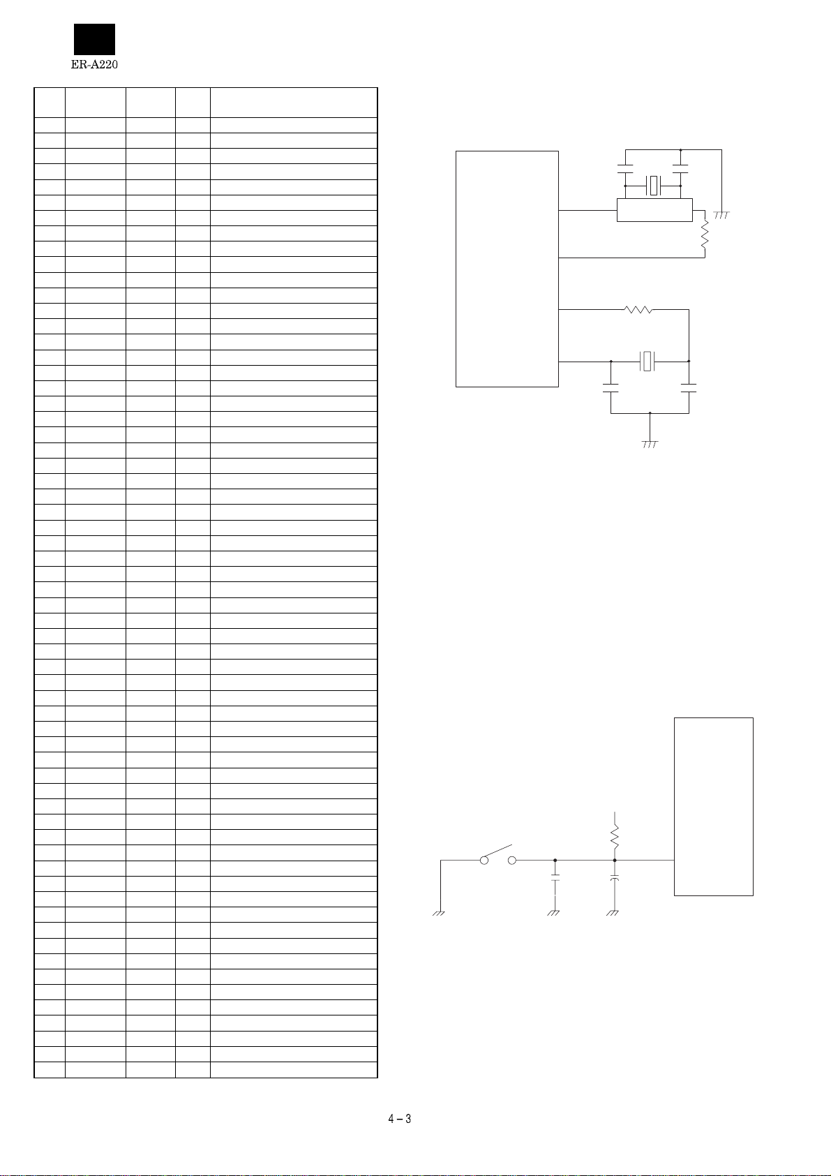
3. Clock generator
1) CPU
Two oscillators are connected to the CPU.
The basic clock X3 is supplied from a 12MHz oscillator.
The 12Mhz basic clocks are formed by X3 and W42C21 and inputted
to the Xin pin of the CPU.
If the CPU was not operating properly, the signal does not appear on
this line in most cases.
The sub-clock X1 generates 32.768KHz which is primarily used to
update the internal RTC (real time clock).
During the standby mode, it keeps oscillating to update the clock and
monitoring the power recov-ery.
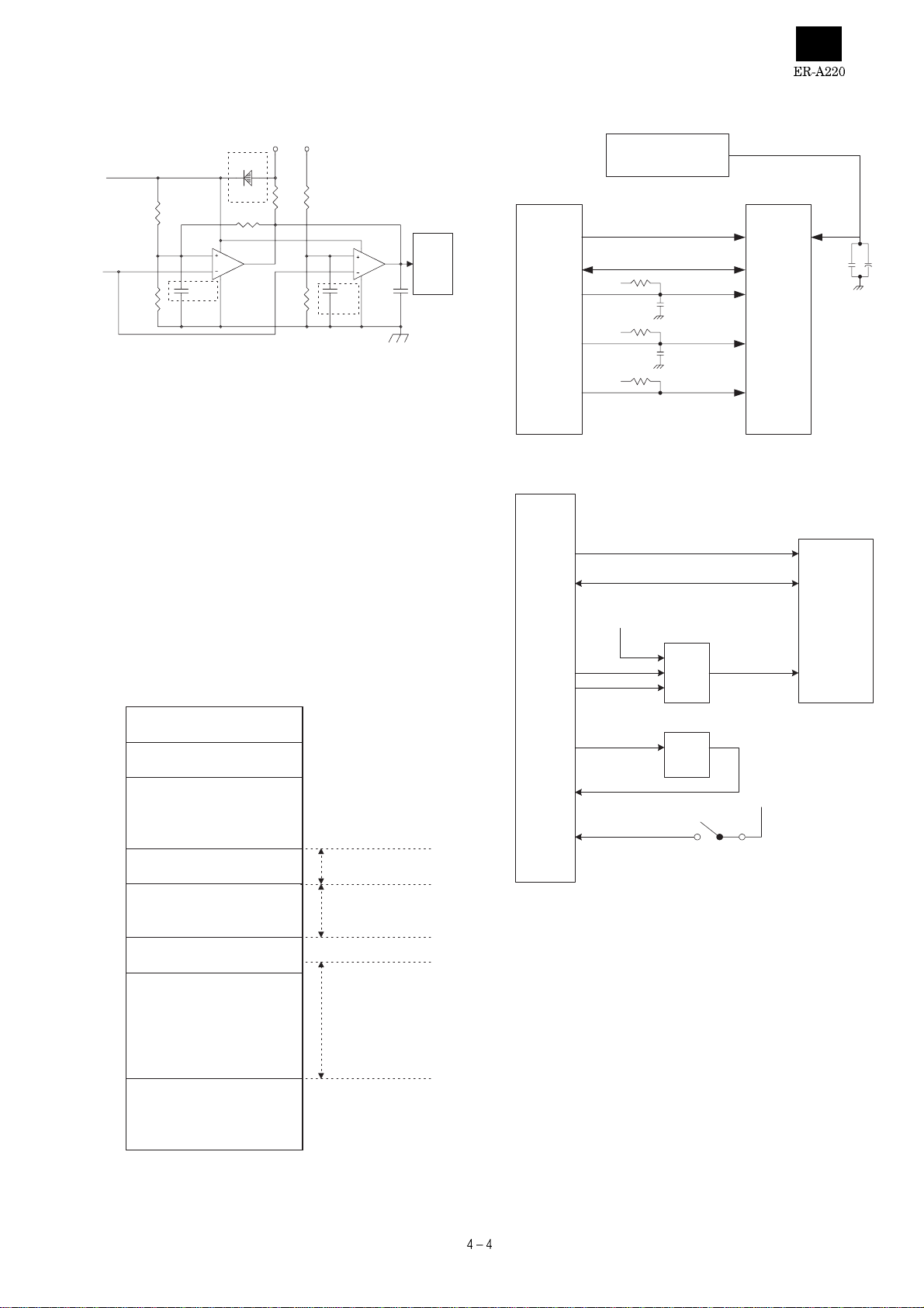
4. Reset circuit
When the mode switch is placed in the "SRV" position, the reset signal
is sent to the CPU to reset the hardware.
11
10
27P
C135
CPU
XIN
X3
12MHz
X1
32.768KHz
12
18P
C134
14
XOUT
XCOUT
XCIN
R110
330
W42C3103G
IC9 R109
0
CPU
R47
/RESET
C14C104
MODE SWITCH
SRV' position
VDD
11
+

5. P-OFF circuit
The P-OFF signal detects two signals by two comparators and sent to
the CPU.
+24V signal : When the mode switch is placed in the OFF position,
the P-OFF output from the comparator: IC10A becomes
low to turn the power off.
When the mode switch is in positions other than OFF,
the P-OFF output from the comparator:IC10A becomes
high to turn the power on.
VCC signal : Though the MODE switch is at ON position, if the logic
power voltage Vcc falls below the specified level, the
P-OFF signal is driven to LOW by the comparator
IC10B.
6. Memory circuit
1) Address map
EP-ROM : Not available as standard equipment. The EP-ROM
socket is provided for rewriting the program for the CPU
internal FLASH-ROM.
2) RAM control
3) EP-ROM (IPL ROM) control
IC2 : EP-ROM (IPL ROM) is used to write data onto the CPU internal
FLASH-ROM.
+24V
VCC
+24V
VCC
R119
56K
R128
2.7K
3
2 1
8
4
IC10A
BA10393
5
6 7
8
4
IC10B
BA10393
R121
2.4KF
R122
13KF
D101
1SS353
P-OFF
C137
0.47uF C138
0.47uF C147
0.1uF
R120
3KF
R123
2.7KF
VREF
(2.495V)
P-OFF
19
Segment latch address
00000h
00400h
05400h
06000h
08000h
40000h
28000h
C0000h
FFFFFh
CPU internal RAM
20kbytes
External S-RAM : 128kbytes
(128kbytes area)
EP-ROM(For IPL) : 256k bytes
(512kbytes area)
CPU internal FLASH-ROM
256kbytes
/CS0 area
30000h - BFFFFh
*30000h - 3FFFFh :
Not used
/CS2 area
08000h - 27FFFh
/CS3 area
06000h - 07FFFh
CPU S-RAM
128K byte
IC3B
A0-A16
D0-7
A0-A16 A0-A16
D0-7 I/O0-7
/CS2
/CS2 /CE
/RD
/RD
/WR /WE
/WR
/OE
Power supply circuit
or
NI-MH battery
VDD
VCC
VDD
VCC
VCC
CPU
IC5B
P71
/HOLD
IC5B
VCC
/CS0 /OE
D0-D7
A0-A17
VCC
SHORT PIN
CNVss SP1
IC2
EP-ROM
(IPL ROM)
D0-D7
A0-A17
/RD

7. Printer control circuit
1) Paper feed motor circuit
A pulse motor is used as the paper feed motor.
Drive sequence of the pulse motor is as follows:
SEQUENCE SIGNAL
A/AB/B
STEP1 High Low Low High
STEP2 High Low High Low
STEP3 Low High High Low
STEP4 Low High Low High
2) Print circuit
Thermal head configuration
As shown in the equivalent circuit in the figure, thermal head con-
sists of heating elements and head drivers which drives and con-
trols those heating elements.
The serial print data input through the DATA IN (D1) is transferred
to the shift register synchronizing with the CLOCK (CP) and stored
in the latch register by the LATCH (LA) signal.
The head conduction signals (print commands 1 ~ 6) turn the gate
on to conduct the heating element corresponding to the print data.
Equivalent circuit of thermal head
Head splitting
The thermal head has 6 strobes so that it is possible to print
dividing up to 6 times. The relationship between the strobes and
heating elements is shown below.
Strobe terminals and conduction heating elements
STB No. Heating element No. Number of dots/STB
11~64 64
2 65 ~ 128 64
3129~192 64
4193~256 64
5257~320 64
6321~384 64
Print data and printing position
384-bit data No.1 ~ 384 transferred by the DTA IN (DI) are printed
in the position shown in the figure.
CPU 74HC32
VH-
VH-
/A
A
B
PH1
PH3
PH2
PH4
/B
To Papper feed motor
LB1843V
74HC123D
LB1843V
STB6 23
VH 1,2,3,26,27,28 dot 384
L-GND 18
P-GND 13,14,15,16,17
STB5 22
STB4 21
STB3 10
STB2 9
STB1 8
/LATCH 5
DATA IN 25
CLOCK 6
DATA OUT 4
VDD 7
NC 19,20,21
TM 11
TM 12
dot 1
654321
Heating element
Latch register
Shift register
Thermister
STB terminal is pulled down inside the IC.
DATA IN
1 2 3 4 ..........................383 384
Paper feed direction
Record paper
Print surface
Data
Printer mechanism
Motor
Print data and printing position

8. Paper take up motor drive circuit
When the MOTOR signal from the CPU is HIGH, Q1 is turned on to
operate the motor.
9. Drawer drive circuit
When the P60 signal from the CPU is HIGH, Q9 is turned on to
operate the solenoid.
10. Buzzer drive circuit
When the BUZ1 signal from the CPU is HIGH, Q6 is turned on to
operate the buzzer.
11. Keyboard circuit
Four P10-13 signals from the CPU are converted into 16 strobe signals by two 74HC138 for use in various functions.
CPU
TA4IN/U
VLED
MOTOR
M
Q1
R46
R45 CN3
D115
CPU
/RST0
+24V
P60 Q9
R164
R163
CN6
C161
ICP103
1.0A
Micro Switch
Drawer
solenoid
C162
CPU
TA4OUT/U
VCC
BUZ1
BZ1
BZ
D7
Q3
CPU
P10-13
P92-97
Key
Matrix Head up
sensor
HC138
P10-13 P10-13
/S8-9
/S0-7
/S0-9
P92-97
Mode
Switch
/S0-7
/S0-9
P91
Paper
feed key
/S1
Receipt
near end
sensor
/S3 /S4
RS232
/CI
signal
/S9
P91
Front
display
74HC374 a,b,c,d,e,f,g,dp
/CS3 Pop-up
display
G1',G2',
G3'G4',G5',
G6',PDSG7
(PDSG7:G7')
/S0 - 9
A',B',C',D',E',F',G',DP'
D0-7 D0-7
/CS3
P90
HC138

1) Keyboard
Scan signal : 10 /S0-9 signals
Return signal : 6 P92-97 signals
The keys are read by the key matrix following the above signals.
2) Mode switch
Scan signal : 8 /S0-7 signals
Return signal : 1 P90 signal
The positions are read by the above signals.
Scan signal /S0 /S1 /S2 /S3 /S4 /S5 /S6 /S7
Mode switch
position SRV PGM (OFF) TIME REG MGR X1/Z1 X2/Z2
3) Paper feed key
Scan signal : 1 /S1 signal
Return signal : 1 P91 signal
The paper feed key is read by the above signals.
4) Head up sensor
Scan signal : 1 /S3 signal
Return signal : 1 P91 signal
The Head up sensor state is read by the above signals.
Head up sensor Head up detected Head up not detected
P91 Low High
5) Receipt near end sensor
Scan signal : 1 /S4 signal
Return signal : 1 P91 signal
The receipt near end sensor state is read by the above signals.
Receipt near end sensor Near end detected Near end not detected
P91 Low High
6) RS232/CI signal detection
Scan signal : 1 /S9 signal
Return signal : 1 P91 signal
The RS232/CI signal is detected by the above signals.
RS232 /CI signal /CI signal detected /CI signal not detected (+5V output)
P91 Low High
7) Display
Scan signal : 10 /S0-9 signals
The above 10 scan signals are used as the following digit signals.
Digit signal :
Scan signal /S0 /S1 /S2 /S3 /S4 /S5 /S6 /S7 /S8 /S9
Digit signal:
Front G1’ G2’ G3’ G4’ G5’ G6’ G7’ G8’ G9’ G10’
Digit signal:
Pop-up G1’ G2’ G3’ G4’ G5’ G6’ G7’
Segment signal :Segment signals: a, b, c, d, e, f, g, and DP are output
by the IC:74HC374, using the data bus signal:D0-7
from the CPU as an input signal and the chip select
signal:/CS3 as a latch signal.
12. RS232 circuit
The signals from the CPU are converted by the MAX211 into the RS232 level to input and output them.
The CI signal allows the output of VCC(+5V) by switching.
CPU MAX211
1
D-SUB 9pin connector
2
3
4
5
6
7
8
9
CD
RD
SD
ER
GND
DR
RS
CS
CI OR VCC(+5V)
R1IN
R2IN
T3OUT
T2OUT
R4IN
R5IN
T1OUT
R3IN
R1OUT
R2OUT
T3IN
R4OUT
T2IN
T1IN
R5OUT
R3OUT
P75
P66
P77
P67
P74
P64
P91
P76
ICP 0.5A
VCC(+5V)
/CD
RD
/SD
/ER
/DR
/RS
/CI
/S5

13. SHORT PIN setting
The ER-A220 has two SHORT PIN settings.
SHORT PIN No. FUNCTION DEFAULT
SP1 Switching between Normal mode/IPL mode Normal mode
SP2 Switching RS232C No.9 pin and Cl/+5V Cl signal
SP1 : Normal mode / IPL mode
VCC
SP1
Normal mode
IPL mode
SP2 : +5V / CI
VCC
/CI
+5V
CI
VCC/CI
VCC
SP1

CHAPTER 5. TEST FUNCTION
1. General
1) This diagnostic program has been developed for diagnosing ma-
chine functions in the field. The program is contained within the
ER-A220.
The diagnostic program is stored in the CPU internal Flash mem-
ory which will be executed by the CPU (M30624FGFP) which re-
quires the following diagnostic operations :
a) Proper power supply voltages are mandatory for logic circuits
(+5V, VDD, POFF, +24V, 5.7V, 7.7V).
b) CPU input/output pins, CPU internal logic, system bus and
RAM must be working properly.
2. Operational procedure
To start the diagnostic program, you must enter the following com-
mand.
3-digit test item number key in the SRV mode
The RAM must be operating properly to go into this mode. This is
necessary because the control jumps to the program area in the SRV
mode. A master reset must be performed before operating the ECR for
the first time. After any option is installed, a program reset is required.
When the master reset or program reset is performed, be sure to
check the printout on the journal paper.
Master reset : Turn power on in the SRV’ mode and change it to
the SRV mode with the PAPER FEED key
pressed.
print : MASTER RESET ***
Program reset : Turn power on in the SRV’ mode and change it to
the SRV mode.
print : PRG. RESET ***
3. Test command list
With the SRV mode and the following test code entry, the test start.
CODE DESCRIPTION
100 Display & Buzzer test
101 Key code test
102 Printer test
104 Keyboard test
105 Mode switch test
106 Printer sensor test
110 Drawer open test
120 External RAM test
121 CPU internal RAM test
130 CPU internal ROM test
140 CPU internal Flash ROM test
500 RS-232 loop back test
550 Sleep mode test
4. Test contents
[1] Display & Buzzer test
1) Key operation
2) Functional description
Display the following message on the front and the rear display
boards.
Front display
Pop-up display
A decimal point shifts from lower number of digit by one digit (per
200m sec.).
Next, display the following segments (for approx. 1 sec.).
Front display
Pop-up display
Repeat the above two kinds of displays.
Sound a buzzer continuously during test.
3) Check items
a) The display must be correctly shown at each position.
b) The luminosity of displays must be uniform and even at each posi-
tion.
c) Abnormal buzzer sound is not allowed.
4) Test termination
Press any key. The test terminates with the test and message printed
[2] Key code test
1) Key operation
100 #/TM/ST
1. 2. 3. 4. 5. 6. 7. 8. 9. 0.
4. 5. 6. 7. 8. 9. 0.
8. 8. 8. 8. 8. 8. 8. 8. 8. 8.
8. 8. 8. 8. 8. 8. 8.
1 0 0
101 #/TM/ST

2) Functional description
Key code, MRS switch (not used in ER-A220) state and Cashier code
are displayed.
3) Check items
a) Key code
HARDWARE CODE" of the following keys will be displayed
ever time the keys are pressed.
"---" indicates that a key is struck twice and also that input data
is not accepted.
[KEY POSITION CODE]
4) Test termination
Change the mode switch position other than SRV position to terminate
the test.
The test terminates with the test and message printed
[3] R/J printer test
1) Key operation
2) Functional description
Display the following message.
Print the following characters.
3) Check items
a) Printed characters must be free of stain and blur.
4) Test termination
This check is terminated automatically.
[4] Keyboard test
1) Key operation
Standard keyboard layout sumcheck data
ER-A220 3383
2) Functional description
Keyboard test is performed with the sumcheck data of key code.
For sumcheck data, data are inputted to the upper four digits befor the
diagnostics code.
The data are compared with the added data which are added until the
final key (TL) is pressed. if the data agree with the added data, the end
print is made. If not, the error print is made.
The sumcheck data is obtained by totalizing all key hardware codes.
MRS switch state (Not used)
Key code
067 051 035 019 003
068 052 036 020 004
066 050 034 018 002
069 053 037 021 005
065 049 033 001
064 048 032 000
017
016
115 099 083
116 100 084
114 098 082
117 101 085
113 097 081
117 096 080
148 132
144 147 131
145 146 130
<ALL KEY>
<ER-A220 STANDARD KEY BOARD LAYOUT>
051 035 019 003
068 052 036 020 004
066 050 034 002
069 053 037 005
065 049 033 001
064 048 032 000
116 100 084
114 098 082
117 101 085
113 097 081
096 080
148 132
144 147 131
145 146 130
1 0 1
102 #/TM/ST
1 2 3 4 5 6 7 8 9 0
3 lines of Z(30 characters) are printed
ZZZZZ • • • • • • ZZZZZZ
3383 104 #/TM/ST
Sumcheck data
1 0 4
Key code

[ALL KEY LAYOUT]
Display the following message on the front display.
3) Check items
a) Check of the display in the test and the content of end print.
4) Test termination
This check is terminated automatically.
The test terminates with the test and message printed
[5] Mode switch test
1) Key operation
2) Functional description
Display the following message on the front display.
When the Mode Switch is switched over in the following order, a
numerical value corresponding to each position of mode switch is
displayed at X.
1 In the OFF mode, the number 9 appears momentarily and then
the power turns off.
2 Turn the mode switch from the X2/Z2 mode to the SRV mode to
finish the test.
The number x should be read in correct order. (When the contacts are
open, the number 9 is displayed.)
3) Check items
a) Check of the display in the test and the content of end print.
4) Test termination
The test terminates with the test and message printed
[6] Printer sensor test
1) Key operation
2) Functional description
State of the paper near end sensor is sensed and displayed.
3) Check items
Displayed Description
XC paper : existed
O paper : Not existed
4) Test termination
Press any key. The test terminates with the test and message printed
[7] Drawer open test (For standard test)
1) Key operation
<ALL KEY>
SUMCHECK DATA = 148 + 132 + 144 + 147 + ········· = 3383
<ER-A220 STANDARD KEY BOARD LAYOUT>
067 051 035 019 003
068 052 036 020 004
066 050 034 018 002
069 053 037 021 005
065 049 033 001
064 048 032 000
017
016
115 099 083
116 100 084
114 098 082
117 101 085
113 097 081
117 096 080
148 132
144 147 131
145 146 130
051 035 019 003
068 052 036 020 004
066 050 034 002
069 053 037 005
065 049 033 001
064 048 032 000
116 100 084
114 098 082
117 101 085
113 097 081
096 080
148 132
144 147 131
145 146 130
Normal end
Error
1 0 4
1 0 4E-----
XXXX
XXXX
Added key code
Added key code
105 #/TM/ST
1 0 5 X
Mode:
x : PGM OFF OP X/ZSRV
0( )
12(9)3
X2/Z2 MGR REGSRV
0X1/Z1
7654
*
1
*
2
Normal end
Error
1 0 5
1 0 5E-----
106 #/TM/ST
1 0 6 X
1 0 6
110 #/TM/ST

2) Functional description
State of the drawer open sensor is sensed and displayed.
3) Check items
X Description
O Drawer open sensor detected. (Drawer opend)
C Drawer open sensor not detected. (Drawer closed)
The ER-A220 is not provided with the open sensor and thus the
letter "C" stays on the display.
a) Check opening of the specified drawer.
4) Test termination
Press any key. The test terminates with the test and message printed
[8] External RAM test
1) Key operation
2) Functional description
Perform the following check for the external RAM 128 KByte SRAM.
Perform the following processes for memory address to be checked
(080000H~27FFFH).
PASS1 : Save memory data.
PASS2 : Write data "00H."
PASS3 : Read and compare data "00H," write data "55H."
PASS4 : Read and compare data "55H," write data "AAH."
PASS5 : Read and compare data "AAH."
PASS6 : Restore the memory data.
If a compare error occurs in the check sequence PASS1-PASS6, an
error print is made. If no error occurs through all address, the check
ends normally.
The following address check is performed further.
Check point address =
10000H , 10001H , 10002H , 10004H , 10008H
10010H , 10020H , 10040H , 10080H ,
10100H , 10200H , 10400H , 10800H ,
11000H , 12000H , 14000H , 18000H ,
20000H
3) Check the following items:
Check the termination printout.
4) Test termination
The test terminates after printing the termination printout.
Termination printout:
Normal termination 120
Abnormal termination Ex – – – – – 120
X = 1: Data check error
2: Address check error
Note: When an error occurs, the error print is performed and the
check is terminated. The error occurrence address is shown in
hexadecimal at positions shown with .
[9] CPU internal RAM test
1) Key operation
2) Functional description
Perform the following check for the CPU internal RAM 20 KByte.
Perform the following processes for memory address to be checked
(00400H~053FFH).
PASS1 : Save memory data.
PASS2 : Write data "00H."
PASS3 : Read and compare data "00H," write data "55H."
PASS4 : Read and compare data "55H," write data "AAH."
PASS5 : Read and compare data "AAH."
PASS6 : Restore the memory data.
If a compare error occurs in the check sequence PASS1-PASS6, an
error print is made. If no error occurs through all address, the check
ends normally. The following address check is performed further.
Check point address =
01000H , 01001H , 01002H , 01004H , 01008H
01010H , 01020H , 01040H , 01080H ,
01100H , 01200H , 01400H , 01800H ,
02000H , 04000HE
3) Check the following items :
Check the termination printout.
4) Test termination
The test terminates after printing the termination printout.
Termination printout:
Normal termination 121
Abnormal termination Ex – – – – 121
X = 1: Data check error
2: Address check error
Note : When an error occurs, the error print is performed and the
check is terminated. The error occurrence address is shown in
hexadecimal at positions shown with .
[10] External ROM (IPL) test
1) Key operation
1 1 0 X
1 1 0
120 #/TM/ST
121 #/TM/ST
130 #/TM/ST

2) Functional description
Sum check of the external ROM for IPL (40000H - 7FFFFH) is per-
formed. If the lower two digits of SUM is 10H, it is normal.
3) Check the following items:
Check the printout after the test.
4) Test termination
The test automatically terminates with termination message.
Normal termination print 130
ROM 27020
Error termination print E – – – – 130
ROM 27020
Note: " " means the ROM version number.
[11] CPU internal FLASH ROM test
1) Key operation
2) Functional description
Sum check of the ROM (C0000H - FFFFFH) is performed. If the lower
two digits of SUM is 10H, it is normal.
3) Check the following items:
Check the printout after the test.
4) Test termination
The test automatically terminates with termination message.
Normal termination print 140
ROM 27020
Error termination print E – – – – 130
ROM 27020
Note : " " means the ROM version number.
[12] RS-232 loop back test
Connect the loop back connector(UKOG-6705RCZZ) to RS232 con-
nector.
1) Key operation
2) Functional description
Control signal check
OUT PUT INPUT
/ER /RS /DR /CI /CD /CS
OFF OFF OFF OFF OFF OFF
OFF ON OFF OFF ON ON
ON OFF ON ON OFF OFF
ON ON ON ON ON ON
Data communication check
Perform 256-byte branch loop back test between SD and RD.
DATA : $00 - $FF
BAUD RATE : 9600 BPS
Display :
3) Test termination
This check is terminated automatically.
The test terminates with the test and message printed
XX: Error code Description
01 ER-DR error
02 ER-CI error
03 RS-CD error
04 RS-CS error
05 SD-RD error (DATA error)
06 SD-RD error (DATA error/Flaming error)
[13] SLEEP MODE test
1) Key operation
2) Functional description
Check the state of SLEEP MODE (Numeric of display: OFF/Decimal
point of display: ON)
And waiting for cancel of SLEEP MODE (Input the any key, Input the
signal of RS232 port)
3) Check item
a) Check the state of SLEEP MODE: Numeric of display:
OFF/Decimal point of display: ON
b) Cancel of SLEEP MODE by input the any key.
4) Test termination
This check is terminated automatically.
The test terminates with the test and message printed
10
7-SEGMENT DISPLAY:
3
140 #/TM/ST
500 #/TM/ST
5 0 0
Normal end
Error
NGRS TEST ER XX
RS TEST OK
550 #/TM/ST
5 5 0

CHAPTER 6. DOWN LOAD FUNCTION
1. General
RAM data can be transmitted in the following two methods.
Save the data before servicing as follows:
ECR ECR
Cable : 9 pin D-SUB – 9 pin D-SUB
Fig. 1-1
ECR ER-02FD
Cable : 9 pin D-SUB – 25 pin D-SUB
Fig. 1-2
2. SIO interface specification
1) Operation: Simplex
2) Line configuration: Direct connect
3) Data rate: 19200/9600(by programming)
4) Sync mode: Asynchronous
5) Checking: Vertical parity (odd)
6) Code: 7 bits (ASCII)
7) Bit sequence: LSB first
8) Line level: RS232 level
9) Data forma:
FIg. 2-1
3. Location of connector pins
ECR-ECR cable
Fig. 3-1
ECR ECR
ECR ER-02FD
Pb1 b2 b3 b4 b5 b6 b7
LSB MSB
Start bit
Parity
bit
Stop
bit
SD 3 SD
RD
CTS
RD
2
6
8
3
2
6
8
55SG
RTS 7
DCD 1
DTR 4
DSR
7
1
4
ECR
CTS
SG
RTS
DCD
DTR
DSR
9PIN D-SUB 9PIN D-SUB
SD : TRANSMITTED DATA
RD : RECEIVED DATA
DTR: DATA TERMINAL READY
DSR: DATA SET READY
RTS: REQUEST TO SEND
DCD: DATA CARRIER DETECTOR
CTS: CLEAR TO SEND
ECR
Other manuals for ER-A220
2
Table of contents
Other Sharp Cash Register manuals

Sharp
Sharp ER-A330 Owner's manual

Sharp
Sharp XE-A301 User manual

Sharp
Sharp UP-3301 User manual

Sharp
Sharp ER-A310 User manual

Sharp
Sharp ER-A410 Owner's manual

Sharp
Sharp XE-A307 User manual

Sharp
Sharp XE-A201 User manual

Sharp
Sharp XE-A106 User manual

Sharp
Sharp XE-A42S User manual

Sharp
Sharp TINSZ2600RCZZ User manual

Sharp
Sharp XE-A120 Quick start guide

Sharp
Sharp XE-A402 User manual

Sharp
Sharp ER-A320 User manual

Sharp
Sharp XE-A137 User manual

Sharp
Sharp XE-A177 Quick manual

Sharp
Sharp XE-A207 Setup guide

Sharp
Sharp ER-A280F User manual

Sharp
Sharp ER-A220 User manual

Sharp
Sharp XEA401 - Cash Register W/THERMAL Printer User manual

Sharp
Sharp ER-A570 Owner's manual