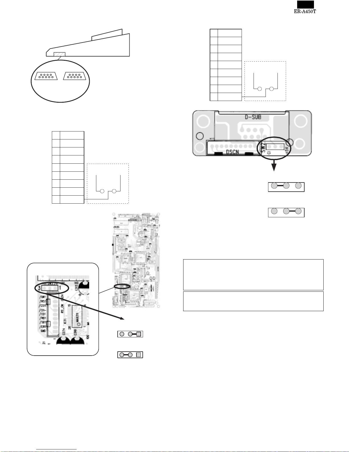
Sharp ER-A450T User manual

SERVICE MANUAL
ELECTRONIC
CASH REGISTER
MODEL ER-A450T
SRV Key : LKGIM7113RCZZ
PRINTER: PR-45M
("U" and "A" version)
CAUTION
EXTREME CAUTION MUST BE TAKEN WHEN SERVICING THIS MACHINE. WHEN THE
MODE SWITCH IS IN THE OFF POSITION, VOLTAGE IS STILL SUPPLIED TO THE ENTIRE
MACHINE.
WHEN WORKING ON THIS MACHINE MAKE SURE THAT THE POWER CORD IS
REMOVED FROM THE WALL OUTLET.
CHAPTER 1. SPECIFICATIONS . . . . . . . . . . . . . . . . . . . . . . . . . . . . . . . . . . 1-1
CHAPTER 2. OPTIONS . . . . . . . . . . . . . . . . . . . . . . . . . . . . . . . . . . . . . . . . . 2-1
CHAPTER 3. SERVICE RESET AND MASTER RESET . . . . . . . . . . . . . . . . 3-1
CHAPTER 4. HARDWARE DESCRIPTION . . . . . . . . . . . . . . . . . . . . . . . . . . 4-1
CHAPTER 5. TEST FUNCTION . . . . . . . . . . . . . . . . . . . . . . . . . . . . . . . . . . . 5-1
CHAPTER 6. DOWN LOAD FUNCTION . . . . . . . . . . . . . . . . . . . . . . . . . . . . 6-1
CHAPTER 7. SERVICE PRECAUTION . . . . . . . . . . . . . . . . . . . . . . . . . . . . . 7-1
CHAPTER 8. CIRCUIT DIAGRAM & PWB LAYOUT . . . . . . . . . . . . . . . . . . . 8-1
PARTS GUIDE
SHARP CORPORATION
CONTENTS
This document has been published to be used
for after sales service only.
The contents are subject to change without notice.
Parts marked with " " are important for maintaining the safety of the set. Be sure to replace these parts with specified
ones for maintaining the safety and performance of the set.

CHAPTER 1. SPECIFICATIONS
1. Appearance/Rating
1) Rating
Power source 120V 10% AC , 60Hz
Power consumption Standby: 14 W
Operating: 37 W (max.)
Operating temperature 32 - 104 °F (0°C - 40°C)
Operating humidity 10% - 90% (RH)
Physical dimensions,
including the drawer 16.5(W) x 16.8(D) x 11.5(H) in.
(420(W) x 427(D) x 292(H)mm)
Weight 27.6 lbs ( 13.5 kg )
2. Keyboard
1) Standard keyboard layout
2) Key top name
Standard Key Top
KEY TOP DESCRIPTION
RECEIPT Receipt paper feed key
JOURNAL Journal paper feed key
0 to 9,00 Numeric keys
•Decimal point key
@/FOR Multiplication / Split-pricing key
CL Clear key
1 to 20 Department keys
PLU/SUB PLU / Subdepartment key
TAX1 SHIFT Tax 1 shift key
TAX2 SHIFT Tax 2 shift key
UPC UPC key
SLIP Slip print key
%1 Percent 1 key
CASH # Cashier code entry key
RCPT Receipt print key
(-) 1 Discount 1 key
NC New charge account balance key
PBLU Previous balance lookup key
FINAL Final key
AMT Amount key
AUTO Automatic sequencing key
RA Received on account key
PO Paid out key
RFND Refund key
VOID Void key
SCALE Scale key
OPEN TARE Open tare key
CH Charge key
CHK Check key
MDSE SBTL Merchandise subtotal key
SBTL Subtotal key
CA/AT Cash/amount tendered key
KEY TOP DESCRIPTION
FS SHIFT Food stamp shift key
FS TEND Food stamp tendered
Optional Key Top
KEY TOP DESCRIPTION
21 to 50 Department keys
TAX3 SHIFT Tax 3 shift key
TAX4 SHIFT Tax 4 shift key
(-)2 - 4 Discount 2 - 4 keys
000 Triple zero key
# Non-add code key
NS No sale key
TAX Tax key
DEPT # Department No. entry key
REPEAT Repeat key
INQ UPC inquiry key
AUTO2 - 10 Automatic sequencing 2 - 10 keys
RA2 Received on account 2 key
PO2 Paid out 2 key
CH2 - 5 Charge 2 - 5 keys
CA2 Cash total 2 key
CONV1 - 4 Currency conversion 1 - 4 keys
CHK2 Check 2 key
RFND SALE Refund sales key
B-DAY Birthday date entry key
NON DELETE Non delete key
PRICE CHANGE Price change key
P1 - 3 UPC price level 1 - 3 keys
SRVC Service key
DEP Deposit key
DEP RFND Deposit refund key
RFNDRCPT SLIP
PO %1
VOID
FINAL
AUTOUPC
RA
PBLU
NC
@/FOR
CL
AMT SCALE
CA/AT
SBTL
CH
PLU/
SUB
CASH
#
OPEN
TARE
TAX1
SHIFT
TAX2
SHIFT
MDSE
SBTL
FS
SHIFT
FS
TEND
CHK
16
17
18
19
20
11
12
13
14
15
6
7
8
9
10
1
2
3
14
5
1
RECEIPT JOURNAL
7
4
1
0
8
5
2
00
9
6
3
Fig. 2-1
1 – 1

3. Mode switch
Fig. 3-1
The key can be removed in the REG or OFF position.
In the SRV’ mode, key inputs are prohibited and no display is present.
[Functions]
•Function for each key position
•SRV’: System reset
•SRV: Service mode (Service programming)
•PGM2: Allows programming of an item that is not changed fre-
quently, in addition to the PGM1 mode programming.
•PGM1: Allows programming of items frequently changed (e.g.
department, PLU pricing, and discount rate setting).
•OP X/Z: Allows X or Z operation by clerks or cashiers.
•REG: Allows registrations.
•MGR: Allows the operations, by authorized person such as a
manager (e.g. correction after transaction finished or
cancellation of entry limits), which are not permitted to
ordinary cashiers.
•X1/Z1: Allows reading and resetting of daily sales total.
•X2/Z2: Allows reading or resetting sales totals for a specified
period.
•OFF: Switching off the display to prevent key board entries.
4. Display
1) Layout
Operator display
Fig. 4-1
7 segment display (LED)
No. of positions 10
Color of display Yellow Green
Character size 14.2 (H) ✕8.0 (W) mm
Customer display (Pop-up display)
Fig. 4-2
7 segment display (LED)
No. of positions 7
Color of display Yellow Green
Character size 14.2 (H) ✕8.0 (W) mm
Display contents
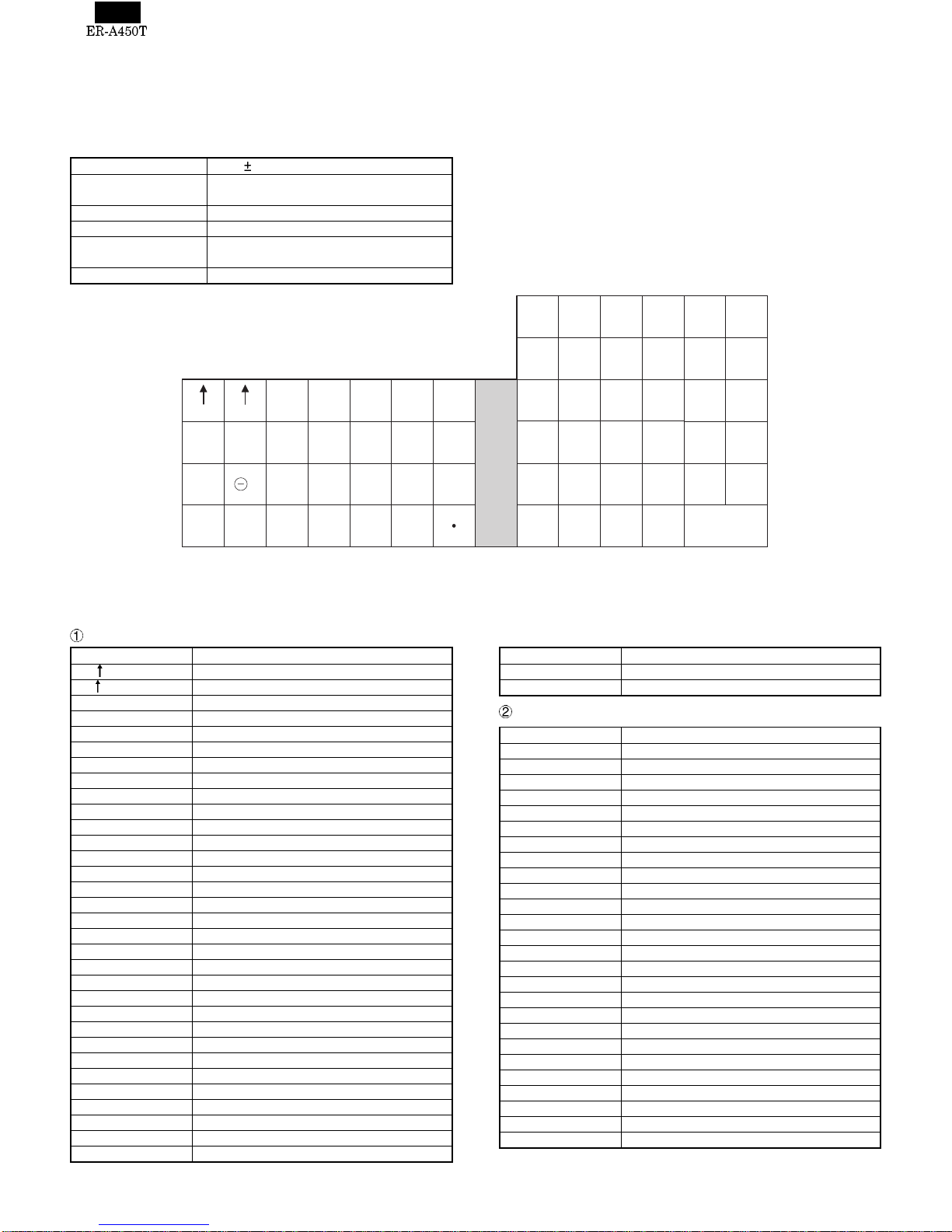
<Segment> Position Description
Amount 1-8
Minus sign 4-10 - : Floating
Error 10 E
PGM Mode 10 P
VOID Mode 10 u
RFND SALE
Mode 1-10 rrrrrrrrrr :
Light up only at the starting of RFND
SALE
CASH,
CHECK,
CHARGE
10 f : Light up when a registration is finalized
by depressing CASH, CHECK,
CHARGE key
SUB TOTAL
/ short tender 10
Change 10 C : Light up whenever the change due
amount appears in the display.
Foreign
Currency
SUB TOTAL
10 c
Food Stamp
Change 10-8 xxF : FS amount
Department 9-10 Not zero-suppressed
PLU 5-10 Not zero-suppressed
Repeat 8 Endless count, starting from 2.
Receipt OFF 9 _
Cashier No. 2-3 - xx - : cashier code (xx = code 1-99)
VP
compulsory 10 U : Light up when the validation printing is
compulsory
Slip
compulsory 10 P : Light up when the slip printing is
compulsory (REG/MGR/VOID mode)
<Decimal point>Position Description
Decimal point 4-1 Based on setuper multiplication.
TAB 4-1 SRV JOB#901
Sentinel 10 PGM JOB#2321
Price Level-3 9 For UPC code entry
Price Level-2 8 For UPC code entry
Scale entry 7 Item unit price
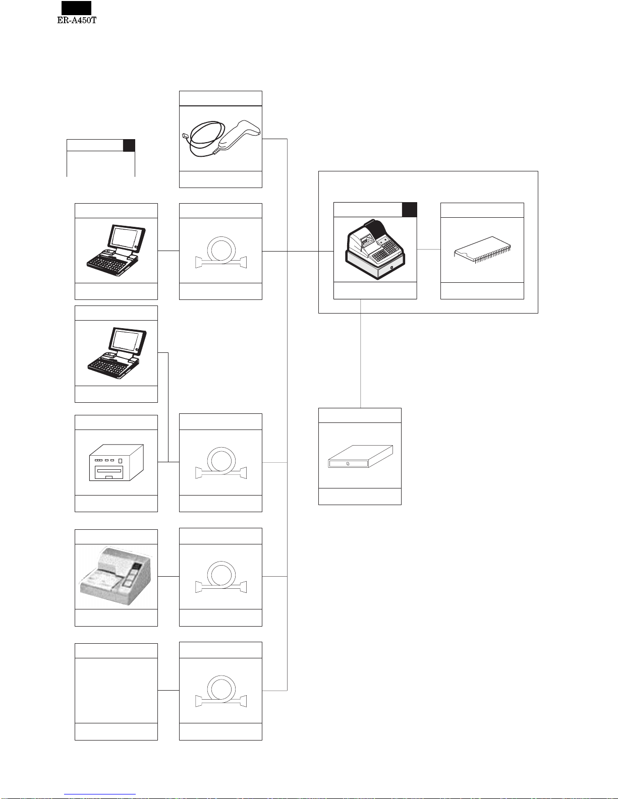
5. Specifications
1) Printer (PR-45M)
•No. of station: 2: Receipt and Journal
•Validation: No
•Printing system: Line thermal
•No. of dot: Receipt: 288 dots
Journal: 288 dots
•Dot pitch: Horizontal: 0.125 mm
Vertical: 0.125 mm
•Font: 10 dots (W) ×24 dots (H)
•Printing capacity: Receipt: Max. 24 characters
Journal: Max. 24 characters
•Character size: 1.25 mm (W) ×3.0 mm (H):
At10×24 dots
•Print pitch: Column distance: 1.5 mm
Row distance: 3.75 mm
•Print speed: Approximate 50 mm/s (13.3 lines/sec)
•Paper feed speed
(Manual feed): Approximate 40 mm/s
•Reliability: Mechanism MCBF 5 million lines
Head life 5 ×10⁷pulses
•Paper end sensor: Yes (Receipt and Journal)
X2/Z2
X1/Z1
MGR
REG
OP,X/Z
PGM1
OFF
PGM2
(SRV)
(SRV')
OP
SM
MA
SRV
PLU/SUB
DEPT REPEAT
RCPT
OFF
P3 P2 $
CID sentinel indicator
Cashier code
$
1 – 2

•Cutter: Manual
•Paper near end sensor: No
•Printing area:
•Print format:
2) Paper
Item Description
Name Heat-quality paper
Roll dimension 44.5 ±0.5 mm in width
Thickness 0.06 mm to 0.08 mm
3) Cutter
•Method: Manual
6. Drawer
1) Specification
(1) Drawer box and drawer
Model name SK-423
Size 420 (W) x 427(L: included lock key) x
112(H: included rubber leg)
Color GRAY 368
Material Metal
Bell -
Release lever Standard equipment; Located at the
bottom
Drawer open sensor Standard equipment
2) Money case
For
"U" version For
"A" version
Separation from the drawer Allowed Allowed
Separation of the coin
compartments from the money case Disallowed Disallowed
Bill separator - YES
Number of compartments 5B/5C 4B/8C
3) Lock
Location of the lock Front
Method of locking
and unlocking Locking: Insert the drawer lock key into
the lock and turn it 90
degrees counterclockwise.
Unlocking: Insert the drawer lock key into
the lock and turn it 90
degrees clockwise.
Key No. SK1-1
(Units : mm)
0.125
14
(112dots)
44.5±0.5
4
44.5±0.5
36
(288dots) 36
(288dots)
(688dots)
4.5
Number of thermal head heater elements 864 dots
1.5 (12dots) 1.5 (12dots)
0.125
0.125
3.0 (24dots)
3.75 (30dots)
3.75 (30dots)
UNIT: mm
Coin compartments
Bill separator
Bill compartments
1 – 3

7. RS232 Interface
1) Port 2 (CH1)
2) Port 1 (CH8)
The No.9 pin signal of the Port 1 (CH8) can be selected between the
/CI signal and the +5V signal by changing the connection of the SW2
(initial value: /CI signal)
NOTE:
Optional bar code reader: When connecting an ER-A6HS1, connect
it to the Port 1 (or 2) and switch the No.9 pin signal to the +5V
signal.
When connecting other RS232 devices to either the Port 1 (or 2),
make sure the No.9 pin signal is proper before connecting the device.
If you want to connect an RS232 device to the ECR with the No.9
pin of the port 1 (or 2) set to +5V, make sure the AC cable of the
ECR is disconnected from the wall outlet to protect the device.
Channel No.:
Port 1(CH8) Channel No.:
Port 2(CH1)
1
2
3
4
5
6
7
8
9
/CD
RD
SD
/ER
GND
/DR
/RS
/CS
/CI
VCC
SW3
on the Main PWB
Pin No.9 : /CI signal (Default)
Pin No.9 :Vcc(+5V) signal
31
SW3
VCC /CI
31
SW3
VCC /CI
1
2
3
4
5
6
7
8
9
/CD
RD
SD
/ER
GND
/DR
/RS
/CS
/CI
+5V
SW2
on the RS connector PWB
SW2
+5V
CI
SW2
+5V
CI
Pin No.9 : /CI signal (Default)
Pin No.9 : +5V signal
1 – 4

CHAPTER 2. OPTIONS
1. System configuration
Fig. 1-1
COMPUTER
LOCAL PURCHASE
OPTION RAM
ER-03RA
BARCODE READER
RS-232
2port
ER-A450T
MASTER MACHINE
CABLE3.5 inch FDD
ER-01/02FD ER-04DW
REMOTE DRAWER
LOCAL PURCHASE
(NOTE1)
This symbol sho ws
NEW MODEL
CABLE
LOCAL PURCHASE
PC UTILITY
ER-A6HS1 or
LOCAL PURCHASE
ER-02FD EXE
CABLESLIP PRINTER
LOCAL PURCHASE
CABLEPRINT DATA
LOCAL PURCHASE
or
LOCAL PURCHASE
LOCAL PURCHASE
Note : Only 2 peripherals max may be connected at any one time.
2 – 1

2. Options (SHARP only)
No. NAME MODEL DESCRIPTION
1 EXPANSION RAM CHIP ER-03RA 512K bytes RAM CHIP
2 REMOTE DRAWER ER-04DW
3 PRESETS LOADER ER-01FD/02FD FD unit
4 KEY TOP KIT ER-11KT7 1 ×1 KEY TOP UNIT
ER-12KT7 1 ×2 KEY TOP UNIT
ER-22KT7 2 ×2 KEY TOP UNIT
ER-11DK7G 1 ×1 DUMMY KEY KIT
ER-51DK7G 5 ×1 DUMMY KEY KIT
5 BARCODE READER ER-A6HS1
3. Service options
No. NAME PARTS CODE PRICE
RANK DESCRIPTION
1 SERVICE KEY AF
2 MODE KEY GRIP COVER AL OP key only
3 DRIP-PROOF KEYBOARD COVER BE Include the switch cover
4 JOURNAL NEAR END SENSOR UNIT BB Q’ty: 1
Screw (Sensor unit – Top cabinet) AA Q’ty: 1
Screw (Sensor unit – Earth wire – Top cabinet) AA Q’ty: 1
Screw (Earth wire – Top cabinet) AA Q’ty: 1
Earth wire AF Q’ty: 1
Connector (2pin) AA Q’ty: 1
5 TEXT PRESET KEYBOARD COVER BH
4. Service tools
No. NAME PARTS CODE PRICE
RANK DESCRIPTION
1 RS-232 LOOP BACK CONNECTOR BU
2 KEY TOP REMOVER AX
32×2 KEY TOP INSTALLING JIG BP
5. Supplies
No. NAME PARTS CODE PRICE
RANK DESCRIPTION
1 Thermal roll paper AY 5 roll/pack
2 Thermal roll paper BA 5 roll/pack (High preservation type)
2 – 2

CHAPTER 3. SERVICE RESET AND MASTER RESET
1. SERVICE reset (Program Loop Reset)
Used to return the machine back to its operational state after a lock-
up has occurred.
Procedure
•Method 1
1) Unplug the AC cord from the wall outlet.
2) Set the mode switch to (SRV′) position.
3) Plug in the AC cord to the wall outlet.
4) Turn to (SRV) position from (SRV′) position.
•Method 2
1) Set the mode switch to PGM2 position.
2) Turn off the AC switch.
3) While holding down JOURNAL FEED key and RECEIPT FEED
key, Turn on the AC switch.
Note: When disassembling and reassembling always power up us-
ing method 1 only. Method 2 will not reset the CKDC8.
Note: SRV programming job#926-B must be set to "4" to allow PGM
program loop reset.
2. Master reset (All memory clear)
There are two possible methods to perform a master reset.
•MRS-1
Used to clear all memory contents and return machine back to its
initial settings and return keyboard back to default keyboard layout.
Procedure
1) Unplug the AC cord from the wall outlet.
2) Set the MODE switch to the (SRV′) position.
3) Plug in the AC cord to the wall outlet.
4) While holding down JOURNAL FEED key, turn to (SRV) position
from (SRV′) position.
•MRS-2
Used to clear all memory and keyboard contents.
This reset returns all programming back to defaults. The keyboard
must be entered by hand.
This reset is used if an application needs different keyboard layout
other than that supplied by a normal MRS-1.
Procedure
1) Unplug the AC cord from the wall outlet.
2) Set the MODE switch to the (SRV′) position.
3) Plug in the AC cord to the wall outlet.
4) While holding down JOURNAL FEED key and RECEIPT FEED
key, turn to (SRV) position from (SRV′) position.
5) Key position assignment:
After the execution of MRS-2, only the RECEIPT FEED and
JOURNAL FEED keys can remain effective on key assignment.
Any key can be assigned on any key position on the main key-
board.
[key setup procedure]
NOTES:
1: When the 0 key is pressed, the key of the key number on display
is disabled.
2: Push the key on the position to be assigned. With this, the key of
the key number on display is assigned to that key position.
Key number Key name Key number Key name
1 Numeric key "0" 10 Numeric key "9"
2 Numeric key "1" 11 Numeric key "00"
3 Numeric key "2" 12 Numeric key "000"
4 Numeric key "3" 13 Decimal point key
5 Numeric key "4" 14 CL key
6 Numeric key "5" 15 @/FOR
7 Numeric key "6" 16 SBTL key
8 Numeric key "7" 17 CA/AT key
9 Numeric key "8"
MRS-2
executed
Key position set Free key
Disable
Free key setup
complete.
*2
*1
0
0
3 – 1

CHAPTER 4. HARDWARE DESCRIPTION
1. Hard ware block diagram
Fig. 1-1
CPU
GATE ARRAY
MPCA7
DRAWER
STANDARD
RAM1
256KB
OPTIONAL
RAM2
512KB
ER-03RA:512KB
STANDARD
ROM
512KB
SWITCH
KEY BOARD
RS232
I/F
1 ports
RS232
I/F
CH1
CKDC8
OPC2
1 LINE
7SEG 7DIG
1 LINE
7SEG 10DIG
CUSTOMER DISPLAY
OPERATER DISPLAY
TPRC1
PRINTER
PR-45M
4 – 1

2. Description of main LSI’s
2-1. CPU (HD6415108-10)
1) Pin configuration
HD6415108-10 pin configuration
Fig. 2-1
RES
NMI
VSS
P10
P11
P12
P13
P14
P15
P16
P17
D0
D1
D2
D3
D4
D5
D6
D7
VSS
A0
A1
A2
A3
A4
A5
A6
A7
1
2
3
4
5
6
7
8
9
10
11
12
13
14
15
16
17
18
19
20
21
22
23
24
25
26
27
28
STBY
MD2
MD1
MD0
VCC
RFSH
LWR
HWR
RD
AS
E
VSS
XTAL
EXTAL
VSS
TXD2
RXD2
TXD1
RXD1
SCK2
UASKC
IRQ1
IRQ0
VCC
AVCC
AN3
AN2
112
111
110
109
108
107
106
105
104
103
102
101
100
99
98
97
96
95
94
93
92
91
90
89
88
87
86
85
P41
P42
P43
P44
P45
P46
P47
VSS
P50
P51
P52
P53
P54
P55
P56
P57/STOP
P60
P61
P62
P63
P64
P65
P66
P67
VSS
AVSS
AN0
AN1
57
58
59
60
61
62
63
64
65
66
67
68
69
70
71
72
73
74
75
76
77
78
78
80
81
82
83
84
A8
A9
A10
A11
A12
A13
A14
A15
VSS
A16
A17
A18
A19
A20
A21
A22
A23
VSS
WAIT
BACK
BREQ
P33
P34
P35
P36
P37
VCC
P40
29
30
31
32
33
34
35
36
37
38
39
40
41
42
43
44
45
46
47
48
49
50
51
52
53
54
55
56
X
4 – 2

2) Block diagram
Fig. 2-2
P47
FTI2
P45
FTI1
P43
P42
P41/TMCI
P40
P37
P36
P35
P34
P33
BREQ
BACK
WAIT
P27/A23
P26/A22
P25/A21
P24/A20
P23/A19
P22/A18
P21/A17
P20/A16
A15
A14
A13
A12
A11
A10
A9
A8
A7
A6
A5
A4
A3
A2
A1
A0
VCC
VCC
VCC
VSS
VSS
VSS
VSS
VSS
VSS
VSS
VSS
AVCC
AVSS
MD2
MD1
MD0
RES
STBY
NMI
AS
RD
HWR
LWR
RFSH
EXTAL
XTAL
E
P17
P16
P15
P14
P13
P12
P11
P10
D7
D6
D5
D4
D3
D2
D1
D0
STOP/P57
P56
FMRS
P54
P53
P52
P51
P50
P67
P66
RS/P65
RR/P64
CD/P63
CS/P62
DR/P61
ER/P60
P73
AN2
AN1
AN0
TXD2
RXD2
TXD1
RXD1
SCK2
IRQ2
IRQ1
IRQ0
H8/500 CPU DTC
Serial
communication
interface x 2ch
8bit timer
16bit free running
timer x 2ch
Refresh controller
Wait state
controller
A/D convertor
Interruption controller
Clock
oscillator Watch
dog timer
Data bus Port 1
Data bus (Lower)
Data bus (Upper)
Address bus
Port 2
Port 3Port 4
Port 5Port 6Port 7Port 8
Address bus
X
4 – 3

3) Pin description
PIN
No. SYMBOL SIGNAL
NAME IN/
OUT FUNCTION
1/RES /RESET IN RESET INPUT from CKDC WUTH
BUFFER
2NMi NMi IN NON-MASKABLE INTERRUPT
INPUT FOR SSP INTERRUPT INPUT
3 VSS VSS GND
4 P10 ERC OUT EVENT READ CANCEL (to CKDC)
5 P11 LDRQ OUT LOAD REQUEST (to CKDC)
6 P12 /SHEN IN SHIFT ENABLE (from CKDC)
7 P13 /FRES OUT FISCAL MEMORY RESET (Nu)
8 P14 BUSY IN FISCAL MEMORY BUSY (Nu)
9 P15 /RDY IN FISCAL MEMORY READY (Nu)
10 P16 PDS IN POP-UP DISPLAY SENSOR (Nu)
11 P17 IN GND
12 D0 D0 I/O DATA BUS 0
13 D1 D1 I/O DATA BUS 1
14 D2 D2 I/O DATA BUS 2
15 D3 D3 I/O DATA BUS 3
16 D4 D4 I/O DATA BUS 4
17 D5 D5 I/O DATA BUS 5
18 D6 D6 I/O DATA BUS 6
19 D7 D7 I/O DATA BUS 7
20 VSS VSS GND
21 A0 A0 OUT ADDRESS BUS 0
22 A1 A1 OUT ADDRESS BUS 1
23 A2 A2 OUT ADDRESS BUS 2
24 A3 A3 OUT ADDRESS BUS 3
25 A4 A4 OUT ADDRESS BUS 4
26 A5 A5 OUT ADDRESS BUS 5
27 A6 A6 OUT ADDRESS BUS 6
28 A7 A7 OUT ADDRESS BUS 7
29 A8 A8 OUT ADDRESS BUS 8
30 A9 A9 OUT ADDRESS BUS 9
31 A10 A10 OUT ADDRESS BUS 10
32 A11 A11 OUT ADDRESS BUS 11
33 A12 A12 OUT ADDRESS BUS 12
34 A13 A13 OUT ADDRESS BUS 13
35 A14 A14 OUT ADDRESS BUS 14
36 A15 A15 OUT ADDRESS BUS 15
37 VSS VSS GND
38 A16 A16 OUT ADDRESS BUS 16
39 A17 A17 OUT ADDRESS BUS 17
40 A18 A18 OUT ADDRESS BUS 18
41 A19 A19 OUT ADDRESS BUS 19
42 A20 A20 OUT ADDRESS BUS 20
43 A21 A21 OUT ADDRESS BUS 21
44 A22 A22 OUT ADDRESS BUS 22
45 A23 A23 OUT ADDRESS BUS 23
46 VSS VSS GND
47 /WAIT /WAIT IN Wait signal from MPCA
48 /BACK /BACK OUT Bus control request acknowledge
49 /BREQ /BREQ IN Bus control request
50 P33 DOPS IN Drawer open sensor signal
51 P34 /DR0 OUT Drawer open drive signal
52 P35 /DR1 OUT Option drawer 1 drive signal
53 P36 NU IN (Nu) GND
54 P37 NU IN (Nu) GND
55 VCC VCC +5V
56 P40 /IFV IN (Nu) pull-up
57 P41 /PTMG IN Printer (PR-45) timing signal from
MPCA
58 P42 /TOF IN (Nu) pull-up
59 P43 /BOF IN (Nu) pull-up
PIN
No. SYMBOL SIGNAL
NAME IN/
OUT FUNCTION
60 P44 /PRST IN Printer (PR-45) Reset signal from
MPCA
61 P45 /NEJ IN Near END signal journal
62 P46 NU IN (NU) GND
63 P47 /NER IN Near END signal receipt
64 VSS VSS GND
65 P50 TRG1 OUT Nu (GND)
66 P51 /PSTOP OUT Nu (GND)
67 P52 /CKDCR2 OUT Nu (GND)
68 P53 OPDS IN Nu (GND)
69 P54 FVPON OUT Nu (GND)
70 P55 FMRS IN Nu (GND)
71 P56 /SLIPLMP OUT Nu (GND)
72 P57 /STOP OUT Nu (GND)
73 P60 /ERS OUT ER signal for RS232 (Equipment
Ready)
74 P61 /DRS IN DR signal for RS232 (Data set Ready)
75 P62 /CSS IN CS signal for RS232 (Clear to Send)
76 P63 /CDS IN CD signal for RS232 (Carrier Detect)
77 P64 /RR OUT RR signal for RS232 (Ready to
Receive) (Nu)
78 P65 /RSS OUT RS signal for RS232 (Request to
Send)
79 P66 (/RI), /CI IN CI signal for RS232 (Calling Indicator)
80 P67 HP IN Nu (GND)
81 VSS VSS GND
82 AVSS AVSS IN GND
83 AN0 Vrf IN Vrf
84 AN1 VHTEST IN VH Test input
85 AN2 VPTEST IN +24V test input
86 AN3 TM IN Thermal head thermistor level test
87 AVCC AVCC IN +5V
88 VCC VCC +5V
89 P80 /iRQ0 IN Interrupt signal 0 from MPCA
90 P81 /iRQ1
(/RSRQ) IN Interrupt signal from OPTION PWB
91 P82 /iRQ2 IN Interrupt signal (Nu) pull-up
92 P83 SCK2 OUT CKDC & FMC i/F sync shift clock
93 P84 RXD IN RS232C RECEIVE DATA
94 P85 TXD OUT RS232C SEND DATA
95 P86 RXD2 IN CKDC, Fiscal memory unit I/F shift
input data
96 P87 TXD2 OUT CKDC, Fiscal memory unit I/F shift
output data
97 VSS VSS GND
98 EXTAL EXTAL IN X-TAL (19.66MHz)
99 XTAL XTAL IN X-TAL (19.66MHz)
100 VSS VSS GND
101 φφ OUT System clock (9.83MHz)
102 E OUT E clock (NU)
103 /AS /AS OUT Address strobe
104 /RD /RD OUT Read
105 /HWR /WR OUT Write
106 /LWR OUT Nu
107 /RFSH /RFSH OUT Refresh cycle (NU)
108 VCC VCC +5V
109 MD0 MD0 IN +5V (MODE 3)
110 MD1 MD1 IN +5V (MODE 3)
111 MD2 MD2 IN GND (MODE 3)
112 /STBY /STBY IN +5V (Nu)
4 – 4

2-2. G.A (MPCA7)
1) Pin configuration
GATE ARRAY (LZ9AH39)
MPCA7
Fig. 2-3
1RF 2JF 3PCUT 4FCUT 5VF 6STAMP
7
SLF
8SLRS 9SLMTD 10RES 11TRG
12TRG
13POFF 14INT1 15HTS1 16SCK1 17STH1 18NU 19NU 20VCC 21GND 22NU 23VRESC 24SLTMG 25SLRST 26AS 27RD 28WR 29
PHAI
30SDT7
31SDT6
32SDT5 33GND 34SDT4 35SDT3
36SDT2
37SDT1 38D0 39D1 40D2
160 NU
159 DOTEN
158 TWAIT
157 NU
156 NU
155 NU
154 NU
153 NU
152 STH2
151 SCK2
150 HTS2
149 SLMTR
148 SLMTS
147 SLMTD
146 RJMTR
145 RAS3
144 NU
143 GND
142 VCC
141 ASKRX
140 NU
139 NU
138 NU
137 RJMTD
136 RJMTS
135 DT5
134 DT6
133 DT7
132 GND
131 DT1
130 DT2
129 DT3
128 DT4
127 RJTMG
126 RJRST
125 RAS1
124 RAS2
123 ROS2
122 ROS1
121 OPTCS
41
D3 42GND 43
D4 44
D5 45
D6 46
D7 47SSPRQ 48
RESET
49
INT2
50
INT3 51RXDI 52TXDI 53SCKI 54IRQ0
55A0
56A1 57A2 58A3 59A4
60A5
61GND 62VCC 63A6 64A7 65A8 66A9 67A10 68A11 69A12 70A13 71A14 72A15
73A16
74A17 75A18 76A19 77A20 78A21
79A22
80NU
120 EXINT0
119 EXINT1
118 EXINT2
117 EXINT3
116 WRO
115 RDO
114 RA15
113 RA16
112 GND
111 RA17
110 RA18
109 EXWAIT
108 WAIT
107 NU
106 MCR1
105 NU
104
DAX1
103 RCKX
102 IRRX
101 GND
100 VCC
99
UATX
98 UARX
97
UASCK
96
IRTX
95 RCO
94 NU
93 NU
92 NU
91 NU
90 MA15
89 TEST
88 MD0
87 MD1
86 IPLON
85 INT4
84 PRST
83 PTMG
82 TRGI
81 A23
4 – 5

2) Block diagram
Fig. 2-4
MTD
MTD
RJMTR
SLMTD
SLMTS
SLMTR
SLMTD
TXDI
SCKI
RXDI
HTS1
SCK1
STH1
HTS2
SCK2
STH2
ROS1
ROS2
RAS1
RAS2
RAS3
OPTCS
AS
RD
WR
RDO
WRO
Φ
RESET
RES
VRESC
POFF
MD0
MD1
WAIT
RJRST
SLRST
*PRST
RJTMG
SLTMG
PTMG
INT4
INT1
INT2
INT3
EXINT0
EXINT1
EXINT2
EXINT3
SDT1~7
DT1~9
TEST
IRQ0
A23~A0
SSPRQ
SLF
SLRS
VF
RF
JF
FCUT
PCUT
STAMP
TRGI
TRG
TRG
DOTEN
IRLON
D0~D7
Φ
Address decode
External CS
Internal CS
RASEL
Image
control
SSP comparison register
BAR.
Buffer
Read/write
control
Divider
CHS
serial select Multiplexer
WAIT
control
CAPS
select
Print gate
Print pulse control
Print mode PMD
INTO
control
Printer control port
Motor
drive
* Output selection with CAPS.
PRST/PTMG.
EXWAIT
I/R Control
IRTX
IRRX
RCI
ASKRX
4 – 6

3) Pin description
Pin
No. Signal
name In/
Out Function
1RF Out Receipt side paper feed solenoid (NU)
2JF Out Journal side paper feed solenoid (NU)
3PCUT Out Printer partial cut signal (NU)
4FCUT Out Printer auto cut signal (NU)
5VF Out Multi line validation paper feed (NU)
6STAMP Out Printer stamp signal (NU)
7SLFS Out Slip printer paper feed singnal (NU)
8SLRS Out Slip printer release signal (NU)
9SLMTD Out Slip printer motor drive signal (NU)
10 RES Out Peripheral output reset
11 TRG Out Dot head trigger signal (NU)
12 TRG Out Dot head trigger signal (NU)
13 POFF In Power off signal input
14 INT1 In (NU)
15 HTS1 Out 8 bit serial port output (for CKDC8)
16 SCK1 Out Serial port shift clock output (for CKDC8)
17 STH1 In 8 bit serial port input (for CKDC8)
18 RAS VZ — Chip select (NU)
19 — — Nu
20 VCC —+5V
21 GND —GND
22 INTMCR — Interrupt (NU)
23 VRESC Out Turns active when reset and power
down is met
24 SLTMG In Slip printer timing signal (NU)
25 SLRST In Slip printer reset signal (NU)
26 AS In Address strobe
27 RD In Read strobe
28 WR In Write strobe
29 φIn (φ) System clock (9.83 MHz)
30 SDT7 Out Slip printer printhead drive signal (dot7)
(NU)
31 SDT6 Out Slip printer printhead drive signal (dot6)
(NU)
32 SDT5 Out Slip printer printhead drive signal (dot5)
(NU)
33 GND —GND
34 SDT4 Out Slip printer printhead drive signal (dot4)
(NU)
35 SDT3 Out Slip printer printhead drive signal (dot3)
(NU)
36 SDT2 Out Slip printer printhead drive signal (dot2)
(NU)
37 SDT1 Out Slip printer printhead drive signal (dot1)
(NU)
38 D0 I/O Data bus 0
39 D1 I/O Data bus 1
40 D2 I/O Data bus 2
41 D3 I/O Data bus 3
42 GND —GND
43 D4 I/O Data bus 4
44 D5 I/O Data bus 5
45 D6 I/O Data bus 6
46 D7 I/O Data bus 7
47 SPRQ Out SSP interrupt request to CPU
48 RESET In MPCA reset
49 SHEN In Shift enable from CKDC8
50 INT3 In Interrupt signal (Nu)
Pin
No. Signal
name In/
Out Function
51 RXD2 Out 8 bit serial port output to CPU
52 TXD2 In 8 bit serial port input from CPU
53 SCK2 In Serial port shift clock input from CPU.
54 IRQ0 Out Interrupt request to CPU
55 A0 In Address bus 0
56 A1 In Address bus 1
57 A2 In Address bus 2
58 A3 In Address bus 3
59 A4 In Address bus 4
60 A5 In Address bus 5
61 GND —GND
62 VCC —+5V
63 A6 In Address bus 6
64 A7 In Address bus 7
65 A8 In Address bus 8
66 A9 In Address bus 9
67 A10 In Address bus 10
68 A11 In Address bus 11
69 A12 In Address bus 12
70 A13 In Address bus 13
71 A14 In Address bus 14
72 A15 In Address bus 15
73 A16 In Address bus 16
74 A17 In Address bus 17
75 A18 In Address bus 18
76 A19 In Address bus 19
77 A20 In Address bus 20
78 A21 In Address bus 21
79 A22 In Address bus 22
80 LCDC — LCD CS (NU)
81 A23 In Address bus 23
82 TRGI In Dot pulse control/drive signal (NU: GND)
83 PTMG Out Printer timing signal to CPU
84 PRST Out Printer reset signal to CPU
85 RDY In Ready from FMC unit
86 IPLON In To option connector (NU) +5V
87 MD1 In Mode select input (GND)
88 MD0 In Mode select input (GND)
89 TEST In +5V
90 MA15 — Image address 15
91 MA18 —Nu
92 MA19 —Nu
93 RCVRDY1 —Nu:+5V
94 RCVRDY2 —Nu:+5V
95 RC0 —Remote control encord signal for CPU
(NU)
96 IRTX — I/R output for LED (NU)
97 UASCK — I/R serial data shift clock (NU)
98 UARX — I/R serial data for CPU (NU)
99 UATX — I/R serial data from CPU (NU) +5V
100 VCC —+5V
101 GND —GND
102 IRRX — I/R input from I/R unit (NU) +5V
103 RCI — I/R input from I/R unit (NU) +5V
104 DAX1 — System clock (NU)
105 DAX2 —Nu
106 MCR1 —Nu
4 – 7

Pin
No. Signal
name In/
Out Function
107 MCR2 —Nu
108 WAIT Out Wait request signal
109 EXWAIT In External wait control input signal (NU)
+5V
110 RA18 Out Nu
111 RA17 Out Nu
112 GND — GND
113 RA16 Out Nu
114 RA15 Out Nu
115 RDO Out Expansion RD signal Option
116 WRO Out Expansion WR signal
117 EXINT3 In RS232C /CD interrupt
118 EXINT2 In Option PWB (PULL UP)
119 EXINT1 In RS232C /CI interrupt
120 EXINT0 In Option PWB (PULL UP)
121 OPTCS Out Chip select base signal for expansion
option
122 ROS1 Out ROM 1 chip select signal
123 ROS2 Out ROM 2 chip select signal (NU)
124 RAS2 Out RAM 2 chip select signal
125 RAS1 Out RAM 1 chip select signal
126 RJRST In Printer reset signal
127 RJTMG In FOR TPRC (NU) +5V
128 DT4 Out Printer dot signal 4 (NU)
129 DT3 Out Printer dot signal 3 (NU)
130 DT2 Out Printer dot signal 2 (NU)
131 DT1 Out Printer dot signal 1 (NU)
132 GND — GND
133 DT7 Out Printer dot signal 7 (NU)
134 DT6 Out Printer dot signal 6 (NU)
135 DT5 Out Printer dot signal 5 (NU)
136 MTD Out Printer motor drive signal (NU)
137 MTD Out Printer motor drive signal (NU)
138 DOT9 Out Printer dot signal 9 (NU)
139 DOT8 Out Printer dot signal 8 (NU)
140 SYNC — Nu (+5V)
141 ASKRX — I/R input from I/R unit (NU) Pull-up
142 VCC — +5V
143 GND — GND
144 — — Nu
145 RAS3 Out Nu
146 RJMTR In Printer motor lock detection signal (NU)
GND
147 SLMTD Out Nu
148 SLMTS Out Nu
149 SLMTR In GND
150 HTS2 Out Serial output to FMC unit
151 SCK2 Out Serial clock to FMC unit
152 STH2 In Serial input to FMC unit
153 — — Nu
154 — — Nu
155 — — Nu
156 — — Nu
157 — — Nu
158 LCDWT IN TPRC wait signal
159 DOTEN Out Dot drive enable signal (Nu)
160 RASP —Nu
2-3. CKDC8
1) Pin configulation
2) Pin assignment (CKDC8)
Pin
No. SYMBOL SIGNAL
NAME IN/
OUT FUNCTION
1 DP DP OUT DISPLAY SEGMENT Dp
2 A SA OUT DISPLAY SEGMENT a
3 B SB OUT DISPLAY SEGMENT b
4 C SC OUT DISPLAY SEGMENT c
5 D SD OUT DISPLAY SEGMENT d
6 E SE OUT DISPLAY SEGMENT e
7 F SF OUT DISPLAY SEGMENT f
8 G SG OUT DISPLAY SEGMENT g
9 VSS0 GND GND
10 VDD0 VDD VDD
11 KR4 KR4 IN KEY RETURN 4
12 KR10 KR10 IN KEY RETURN (feed clerk
MRS sw)
13 KR11 KR11 IN KEY RETURN (MODE sw)
14 KR8 NU IN GND
15 HTS HTS IN
16 STH STH OUT
17 /SCK /SCK IN SHIFT CLOCK
18 ST0 ST0 OUT KEY STROBE 0
19 ST1 ST1 OUT KEY STROBE 1
20 ST2 ST2 OUT KEY STROBE 2
21 ST3 ST3 OUT KEY STROBE 3
22 ST4 ST4 OUT KEY STROBE 4
23 ST5 ST5 OUT KEY STROBE 5
24 VDD1 VDD VDD
25 AXSS GND GND
26 KR9 NU GND
27 KR0 KR0 IN KEY RETURN 0
28 KR1 KR1 IN KEY RETURN 1
29 KR2 KR2 IN KEY RETURN 2
30 KR3 KR3 IN KEY RETURN 3
31 KR5 KR5 IN KEY RETURN 5
NU
NU
G10
G9
G8
G7
G6
G5
G4
G3
G2
G1
BUZ
/POFF
NU
ST8
1
2
3
4
5
6
7
8
9
10
11
12
13
14
15
16
DP
SA
SB
SC
SD
SE
SF
SG
GND
VDD
KR4
KR10
KR11
NU
HTS
STH
48
47
46
45
44
43
42
41
40
39
38
37
36
35
34
33
ST7
ST6
/RESETS
/SHEN
ERC
LDRQ
GND
GND
/RES0
VDD
GND
KR7
64
63
62
61
60
59
58
57
56
55
54
53
52
51
50
49
/SCK
ST0
ST1
ST2
ST3
ST4
ST5
VDD
GND
NU
KR0
KR1
KR2
KR3
KR5
KR6
17
18
19
20
21
22
23
24
25
26
27
28
29
30
31
32
CKDC8
4 – 8

Pin
No. SYMBOL SIGNAL
NAME IN/
OUT FUNCTION
32 KR6 KR6 IN KEY RETURN 6
33 KR7 KR7 IN KEY RETURN 7
34 AVRF GND
35 AVDD VDD
36 /RESET /RES0 IN
37 XT2 32.768 KHz
38 XT1
39 IC GND
40 X2 4.19 MHz
41 X1
42 VSS1 GND
43 LDRQ LDRQ IN LORD REQUEST
44 ERC ERC IN EVENT READ CANCEL
45 SHEN /SHEN OUT SHIFT ENABLE
46 /RES1 /RESETS OUT SYSTEM TO RESET
47 ST6 ST6 OUT KEY STROBE 6
48 ST7 ST7 OUT KEY STROBE 7
49 ST8 ST8 OUT KEY STROBE 8
50 ST9 NU OUT KEY STROBE 9
51 /POFF /POFF IN POWER OFF
52 BUZ BUZ OUT BUZZER
53 T0 G1 OUT DISPLAY DIGIT 1
54 T1 G2 OUT DISPLAY DIGIT 2
55 T2 G3 OUT DISPLAY DIGIT 3
56 T3 G4 OUT DISPLAY DIGIT 4
57 T4 G5 OUT DISPLAY DIGIT 5
58 T5 G6 OUT DISPLAY DIGIT 6
59 T6 G7 OUT DISPLAY DIGIT 7
60 T7 G8 OUT DISPLAY DIGIT 8
61 T8 G9 OUT DISPLAY DIGIT 9
62 T9 G10 OUT DISPLAY DIGIT 10
63 T10 NU OUT DISPLAY DIGIT 11
64 ID NU OUT DISPLAY SEGMENT
2-4. TPRC1 (F258024PC)
1) General
TPRC1 is the LSI circuit of the peripheral circuits of the microcom-
puter required for thermal printer control.
Fig. 2-6
The CPU is designed for use with H8/500. The bus I/F, however, is
not restricted to the design concept.
The printer is designed mainly for use with PR-58. However, the
thermalhead composition (the dot number and the block number) is
rather flexible.
1. Auto cutter (Option)
2. Pulse motor
3. Thermalhead
4. Switch
CG ROM
PHAI
INT
WAIT
RD
WR
D0~7
A0~23
CPU
(H8/500)
POF,RES
TPRC1
PB RAM
(SRAM)
Auto cutter Pulse motor
Thermal
head
Switch
sensor
SO
CLOCK
SI
LATCH
ST1~4
HCD
PHUP,PSP,
PST,POP
CTAO,CTBO
PFP,PCRES
XRS,XJS
RVPON,JVPON
RTRM,PTJM
BA0~15
BD0~2
BRD
BWR
BRAS
(BRAS)
4 – 9

2) Pin configuration
Fig. 2-7
1
GND
2
GND
3ST1 4
5ST2 6ST3 7ST4 8ST5 9
ST6
10LATCH 11
12
13
14SI 15
SO
16CLOCK 17INHDEC 18CSEN 19TEST2 20
21
22
23
24
TEST1
25D0 26D1 27D2 28
D3
29D4 30
31
32
33D5 34D6 35D7 36A0 37A1 38A2 39NU 40
160
159
158 RESET
157 BRAS
156 BRAS
155 BD0
154 BD1
153 BD2
152
151
150
149 BD3
148 BD4
147
146 BD5
145 BD6
144 BD7
143 BA0
142
141
140
139 PHAI
138 BA1
137 BA2
136 BA3
135 BA4
134 BA5
133 BA6
132
131
130
129 BA7
128 BA8
127 BA9
126 BA10
125 BA11
124 BA12
123 P.P
122
121
41
42BACK 43A3 44A4 45A5 46A6 47A7 48A8 49A9 50
51
52
53A10 54A11 55A12 56A13 57A14 58A15 59A16 60
61
62
63A17 64A18 65A19 66A20 67A21 68A22 69A23 70
71
72RD 73WR 74
AS 75POF 76INT 77
WO 78
79BREQ 80
120
PTJM
119
PTRM
118 BA13
117 BA14
116
BA15
115
BRD
114
BWR
113 CGS
112
111
110
109 JAS
108
JBS
107 JCS
106 JDS
105 RAS
104 RBS
103
102
101
100
99
98
97 RCS
96 RDS
95
CTAO
94
CTBO
93
VHCOM
92 JVPON
91
90
89
88 RVPON
87
PFP
86
PCRES
85 PHUP
84 JPE
83
ROE
82
EBACK
81
EBREQ
GND
GND
GND
GND
VCC
VCC
VCC
VCC
GND
GND
GND
INTI
WI
GND
GND
GND
VCC
VCC
VCC
GND
GND
INH
NU
GND
GND
GND
VCC
VCC
VCC
VCC
VCC
GND
GND
GND
GND
GND
GND
GND
GND
GND
VCC
VCC
VCC
GND
GND
GND
GND
NU
GND
4 – 10

3) Block diagram
TPRC1 BLOCK DIAGRAM
Fig. 2-8
4) Pin description
Pin
No. Signal
name In/Out Function
1 GND — GND
2 GND — GND
3ST1 O Head drive strobe signal 1
4 GND — GND
5ST2 O Head drive strobe signal 2
6ST3 O Head drive strobe signal 3
7ST4 O Head drive strobe signal 4
8ST5 O NU
9ST6 O NU
10 LATCH O Head latch signal
11 GND — GND
12 GND — GND
13 GND — GND
14 SI I Data return line, thermalhead -- TPRC1
15 SO O Send data from TPRC1 to thermalhead
Data from PB-RAM or zero data are
outputted at the falling of CLOCK signal.
16
16 CLOCK O Thermalhead CLOCK signal
SO is outputted at the edge of I Ä O,
and is taken at the edge of o Ä I.
17 INHDEC I GND
Pin
No. Signal
name In/Out Function
18 CSEN I GND
19 TEST2 I +5V internal counter timer test pin
20 Vcc — +5V
21 Vcc — +5V
22 Vcc — +5V
23 Vcc — +5V
24 TEST1 I +5V internal counter timer test pin
25 D0 I/O Data bus 0: Internal register, print buffer
data IO
26 D1 I/O Data bus 1: Internal register, print buffer
data IO
27 D2 I/O Data bus 2: Internal register, print buffer
data IO
28 D3 I/O DAta bus 3: Internal register, print buffer
data IO
29 D4 I/O Data bus 4: Internal register, print buffer
data IO
30 GND — GND
31 GND — GND
32 GND — GND
33 D5 I/O Data bus 5: Internal register, print buffer
data IO
MOTOR
CONTROL
HEAD
I/F
MISC.
TEST
CIRCUIT
CUTTER
CONTROL
PB I/F UNIT
SYSTEM
I/F
PORT
PDCTLU
DECODEK UNIT
HEAD CONTROL
TIMER UNIT
MOTOR CONTROL
TIMER UNIT
CUTTER CONTROL
TIMER UNIT
CLOCK
GEN.
INTERRUPT
CIRCUIT HOST BUS I/F UNIT
INHBEC
CSEN
CGS
RD,WR
A0~23
D0~7
WO
WI
INT
INTI
PHAI
(
Φ)
BD0~7
BA0~15
BRAS,BRAS
BRD,BWR
RES
POF,INH
POP,PHUP,PFP,PCRES
PTRM,PTJM
CLOCK,SO,ST1~5,HCO
SI
EBAK,EPEQ
EBRK,EACK
RVPON,JVPON,
RAS,RBS,RCS,RDS,
JAS,JBD,JCS,JDS
TEST1,TEST2
CTAO,CTBO
4 – 11

Pin
No. Signal
name In/Out Function
34 D6 I/O Data bus 6: Internal register, print buffer
data IO
35 D7 I/O Data bus 7: Internal register, print buffer
data IO
36 A0 I Address bus 0
37 A1 I Address bus 1
38 A2 I Address bus 2
39 TPRCRQ2 — Request signal
40 INTI I +5V
41 WI I +5V
42 BACK I BACK
43 A3 I Address bus 3
44 A4 I Address bus 4
45 A5 I Address bus 5
46 A6 I Address bus 6
47 A7 I Address bus 7
48 A8 I Address bus 8
49 A9 I Address bus 9
50 GND — GND
51 GND — GND
52 GND — GND
53 A10 I Address bus 10
54 A11 I Address bus 11
55 A12 I Address bus 12
56 A13 I Address bus 13
57 A14 I Address bus 14
58 A15 I Address bus 15
59 A16 I Address bus 16
60 Vcc — +5V
61 Vcc — +5V
62 Vcc — +5V
63 A17 I Address bus 17
64 A18 I Address bus 18
65 A19 I Address bus 19
66 A20 I Address bus 20
67 A21 I Address bus 21
68 A22 I Address bus 22
69 A23 I Address bus 23
70 GND — GND
71 GND — GND
72 RD I Read strobe signal: Gate enable of data
bus D0 - D7 tri-state buffer
73 WR I Write strobe signal: Write enable into
the internal register and the print buffer.
74 AS I AS
75 POF I Power off signal
76 INT O Interrupt signal
77 WO O Wait request signal to the CPU
78 INH I Head drive inhibit
79 BREQ O Bus request to CPU
80 — — NU
81 EBREQ I Bus request from option
82 EBACK O Bus acknowledge to option
83 RPE I Receipt paper empty
Pin
No. Signal
name In/Out Function
84 JPE I Journal paper empty
85 PHUP I Printer head up
86 PCRES I Auto cutter unit reset signal input (Nu)
87 PFP I Auto cutter unit FP signal input (Nu)
88 RVPON O Receipt side paper feed pulse motor
common power control signal (Nu)
89 GND — GND
90 GND — GND
91 GND — GND
92 JVPON O Journal side paper feed pulse motor
common power control signal (Nu)
93 VHCOM O Head drive common power control
94 CTBO O Cutter motor control signal (Nu)
95 CTAO O Cutter motor control signal (Nu)
96 RDS O Receipt side paper feed pulse motor
drive signal, phase D
97 RCS O Receipt side paper feed pulse motor
drive signal, phase C
98 GND — +5V
99 Vcc — +5V
100 Vcc — +5V
101 Vcc — +5V
102 Vcc — +5V
103 Vcc — +5V
104 RBS O Receipt side paper feed pulse motor
drive signal, phase B
105 RAS O Receipt side paper feed pulse motor
drive signal, phase A
106 JDS O Journal side paper feed pulse motor
drive signal, phase D
107 JCS O Journal side paper feed pulse motor
drive signal, phase C
108 JBS O Journal side paper feed pulse motor
drive signal, phase B
109 JAS O Journal side paper feed pulse motor
drive signal, phase A
110 GND — GND
111 GND — GND
112 GND — GND
113 CGS O NU
114 BWR O PB-RAM write strobe signal
115 BRD O PB-RAM read strobe signal
116 BA15 O NU
117 BA14 O Address 14 for PB-RAM
118 BA13 O Address 13 for PB-RAM
119 PTRM I Receipt motor connector sensor signal
120 PTJM I Journal motor connector sensor signal
121 GND — GND
122 GND — GND
123 POPI O GND
124 BA12 O Address bus 12 for PB-RAM
125 BA11 O Address bus 11 for PB-RAM
126 BA10 O Address bus 10 for PB-RAM
127 BA9 O Address bus 9 for PB-RAM
128 BA8 O Address bus 8 for PB-RAM
129 BA7 O Address bus 7 for PB-RAM
4 – 12
Other manuals for ER-A450T
4
Table of contents
Other Sharp Cash Register manuals

Sharp
Sharp XE-A110 User manual

Sharp
Sharp XE-A402 User manual

Sharp
Sharp XE-A301 User manual

Sharp
Sharp ER-A310 User manual

Sharp
Sharp XE-A20S User manual

Sharp
Sharp ER-A410 User manual

Sharp
Sharp XE-A152 User manual

Sharp
Sharp XE-A207W Quick manual

Sharp
Sharp XE-A302 User manual

Sharp
Sharp XE-A101 User manual

Sharp
Sharp UP-3301 User manual

Sharp
Sharp ER-A450T User manual

Sharp
Sharp XE-A101 User manual

Sharp
Sharp ER-A55R1 User manual

Sharp
Sharp ER-87MA User manual

Sharp
Sharp XE-A207W Operating and maintenance manual

Sharp
Sharp XE-A137-WH Operation Quick manual

Sharp
Sharp ER-2722A User manual

Sharp
Sharp ER-A570 Owner's manual

Sharp
Sharp XE-A507 User manual