ER-A520U/ER-A530U HARDWARE DESCRIPTION
– 8 –
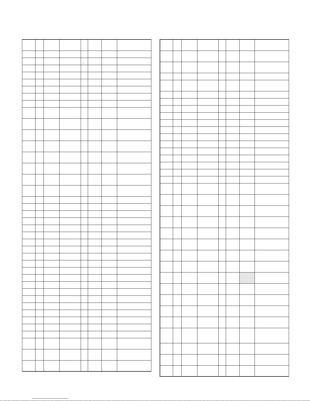
3. CPU PIN TABLE
M16C/80 PORT USED IN PROCESSOR MODE: MICROPROCESSOR MODE (SEPARATE BUS 8bit WIDTH)
PORT PIN
No. Pin
name Signal
name I/O Initial
value After
POFF Function
P00 122 D0 D0 I/O −In DATA BUS D0
P01 121 D1 D1 I/O−In DATA BUS D1
P02 120 D2 D2 I/O −In DATA BUS D2
P03 119 D3 D3 I/O −In DATA BUS D3
P04 113 D4 D4 I/O −In DATA BUS D4
P05 112 D5 D5 I/O −In DATA BUS D5
P06 111 D6 D6 I/O −In DATA BUS D6
P07 110 D7 D7 I/O −In DATA BUS D7
P10 109 P10 RAS O L Out L RECEIPT
PAPER FEED A
P11 108 P11 RBS O L Out L RECEIPT
PAPER FEED B
P12 107 P12 RCS O L Out L RECEIPT
PAPER FEED C
P13 106 P13 RDS O L Out L RECEIPT
PAPER FEED D
P14 105 P14 JAS O L Out L JOURNAL
PAPER FEED A
P15 104 P15
/INT3# JBS O L Out L JOURNAL
PAPER FEED B
P16 103 P16
/INT4# JCS O L Out L JOURNAL
PAPER FEED C
P17 102 P17
/INT5# JDS O L Out L JOURNAL
PAPER FEED D
P20 101 A0 A0 O −Out L Address Bus A0
P21 100 A1 A1 O −Out L Address Bus A1
P22 99 A2 A2 O −Out L Address Bus A2
P23 98 A3 A3 O −Out L Address Bus A3
P24 97 A4 A4 O −Out L Address Bus A4
P25 96 A5 A5 O −Out L Address Bus A5
P26 95 A6 A6 O −Out L Address Bus A6
P27 94 A7 A7 O −Out L Address Bus A7
P30 92 A8 A8 O −Out L Address Bus A8
P31 85 A9 A9 O −Out L Address Bus A9
P32 84 A10 A10 O −Out L Address Bus A10
P33 83 A11 A11 O −Out L Address Bus A11
P34 82 A12 A12 O −Out L Address Bus A12
P35 81 A13 A13 O −Out L Address Bus A13
P36 80 A14 A14 O −Out L Address Bus A14
P37 79 A15 A15 O −Out L Address Bus A15
P40 78 A16 A16 O −Out L Address Bus A16
P41 77 A17 A17 O −Out L Address Bus A17
P42 75 A18 A18 O −Out L Address Bus A18
P43 73 A19 A19 O −Out L Address Bus A19
P44 72 A20
/CS3# A20 O −Out L Address Bus A20
P45 71 A21
/CS2# A21 O −Out L Address Bus A21
P46 70 A22
/CS1# A22 O −Out L Address Bus A22
P47 69 A23#
/CS0# A23# O −Out L Address Bus A23
P50 65 WR# WR# O −Out L WRITESTROBE
SIGNAL
P51 64 BHE# BHE# O −Out L NOT USED
P52 63 RD# RD# O −Out L READ STROBE
SIGNAL
P53 62 BCLK BCLK O −Out L BCLK CLOCK
P54 55 HLDA# HLDA# O −Out L NOT USED
P55 54 HOLD# HOLD# I −In NOT USED
P56 53 ALE ALE O −Out L NOT USED
P57 52 RDY# RDY# I −In NOT USED
P60 47 RTS0# RS2# O H In RS-232 RS2
P61 46 CLK0
CI2#
I−In RS-232 CI2
P62 45 RxD0 RD2 I −In RS-232 RD2
P63 44 TxD0 TD2 O H In RS-232 TD2
P64 43 RTS1# RS1# O H In RS-232 RS1
P65 42 CLK1 CI1# I −In RS-232 CI1
P66 40 RxD1 RD1 I −In RS-232 RD1
P67 38 TxD1 TD1 O H In RS-232 TD1
P70 37 P70/
TA0out KR0# I −In KEY RETURN
SIGNAL 0
P71 36 P71/
TA0in KR1# I −In KEY RETURN
SIGNAL 1
P72 35 P72/
TA1out KR2# I −In KEY RETURN
SIGNAL 2
P73 34 P73/
TA1in
KR3#
I−In KEY RETURN
SIGNAL 3
P74 33 P74/
TA2out KR4# I −In KEY RETURN
SIGNAL 4
P75 32 P75/
TA2in KR5# I −In KEY RETURN
SIGNAL 5
P76 31 P76/
TA3out KR6# I −In KEY RETURN
SIGNAL 6
P77 30 P77/
TA3in KR7# I −In KEY RETURN
SIGNAL 7
P80 29 P80/
TA4out BUZZER O L In BUZZER SIG-
NAL
P81 28 P81/
TA4in DSEN I −In DRAWEROPEN
SENSE SIGNAL
P82 27 P82/
INT0# POFF# I −In P-OFF SIGNAL
P83 26 P83
/INT1# SHEN# I −In
UP-P16DP
SHEN# SINGNAL
P84 25 P84
/INT2# I−In NOT USED
P85 24 P85
/NMI# NMI# I −In NMI (CON-
NECTED TO
VDD)
P86 18
P86/
Xcout
Xcout O −Out SUB CLOCK
(32.768kHz)
P87 17 P87/
Xin Xcin I −In SUB CLOCK
(32.768kHz)
P90 7 P90/
CLK3 SCK O L Out L UP-P16DP
CLOCK SIGNAL
PORT PIN
No. Pin
name Signal
name I/O Initial
value After
POFF Function