Sharp LS013B4DN02 User manual

TECHNICAL LITERATURE
For
TFT-LCD Module
Model No. LS013B4DN02
Notice
Mobile Liquid Crystal Display Group
SHARP CORPORATION
No. LCY-12T09303B
Date July. 21st 2009
The technical Literature is subject to change without any prior
notice for the purpose of product improvement.
Please contact Sharp or its representative before designing your
product based on this literature.

SPEC No.
LCY-12T09303B
MODEL No.
LS013B4DN02
PAGE
1
NOTICE
<<Precautions>>
○These specification sheets are the proprietary product of SHARP CORPORATION ("SHARP") and include materials
protected under copyright of SHARP. Do not reproduce or cause any third party to reproduce them in any form or by
any means, electronic or mechanical, for any purpose, in whole or in part, without the express written permission of
SHARP.
○The application examples in these specification sheets are provided to explain the representative applications of the
device and are not intended to guarantee any industrial property right or other rights or license you to use them.
SHARP assumes no responsibility for any problems related to any industrial property right of a third party resulting from
the use of the device.
○SHARP reserves the right to make changes in the specifications, characteristics, data, materials, structures and other
contents described herein at any time without notice in order to improve design or reliability. Contact SHARP in order
to obtain the latest specification sheets before using any SHARP's device. Manufacturing locations are also subject to
change without notice.
Observe the following points when in using any device in this publication. SHARP takes no responsibility
for damage caused by improper use of the devices.
The devices in this publication are designed for use in general electronic equipment designs, such as:
・Personal computers ・Office automation ・Telecommunication equipment
・Test and measurement equipment ・Industrial control
・Audio visual and multimedia equipment ・Consumer electronics
The appropriate design measures should be taken to ensure reliability and safety when SHARP's devices are
used for equipment such as:
・Transportation control and safety equipment(i.e.,aircraft,trains,automobiles,etc.)
・Traffic signals ・Gas leakage sensor breakers
・Alarm equipment ・Various safety devices etc.
○SHARP's devices shall not be used for equipment that requires extremely high level of reliability, such as:
・Military and space applications ・Nuclear power control equipment
・Medical equipment for life support
○SHARP assumes no responsibility for any damage resulting from the use of the device which does not comply with
the instructions and the precautions specified in these specification sheets.
○Contact and consult with a SHARP sales representative for any questions about this device.

SPEC No.
LCY-12T09303B
MODEL No.
LS013B4DN02
PAGE
2
[For handling and system design]
(1) Handle with care as glass is used in this LCD panel. Dropping or contact against hard object may cause cracks or
chips.
(2) Do not scratch the surface of the UV protection film as it is easily damaged.
(3) Water droplets on the UV protection film must be wiped off immediately as they may cause color changes, or other
defects if remained for a long time.
(4) To clean LCD panel surface, wipe clean with absorbent cotton or soft cloth. If further cleaning is needed, use IPA
(isopropyl alcohol) and wipe clean lightly on surface only. Do not use organic solvents as it may damage the LCD
panel terminal area which uses organic material. Also, do not directly touch with finger.
(5) To avoid circuit failure, do not touch panel terminal area.
(6) Do not expose gate driver, etc. on the panel (circuit area outside panel display area) to light as it may not operate
properly. Design that shields gate driver, etc. from light is required when mounting the LCD module.
(7) Support for the LCD panel should be carefully designed to avoid stress that exceeds specification on glass surface.
(8) Panel is susceptible to mechanical stress and such stress may affect the display. Place the panel on flat surface
to avoid stress caused by twist, bend, etc..
(9) When transporting LCD panels, secure them in LCD panel tray to avoid mechanical stress. The tray should be
conductive to protect LCD panels from static charge.
Material used in set or epoxy resin (amine type hardening agent) from packaging, and silicon adhesive
(dealcoholized or oxime) all release gas which may affect quality of UV protection film. Do confirm compatibility with
user materials.
(10) Do not use chloroprene rubber as it generates chlorine gas and affects reliability in LCD panel connective area.
(11) This LCD module is sensitive to electrostatic discharge of 200V or more. Handle with care using cautions for
the followings:
zOperators
Operators must wear anti-static wears to prevent electrostatic charge up to and discharge from human
body.
zEquipment and containers
Process equipment such as conveyer, soldering iron, working bench and containers may possibly generate
electrostatic charge up and discharge. Equipment must be grounded through 100Mohms resistance. Use
ion blower.
zFloor
Floor plays an important role in leaking static electricity generated in human body or equipment. If the floor
is made of insulated material (such as polymer or rubber material), such static electricity may charge.
Proper measure should be taken to avoid static electricity charge (electrostatic earth: 100Mohms).There is
a possibility that the static electricity is charged to them without leakage in case of insulating floor, so the
electrostatic earth:1×10⁸Ωshould be made.

SPEC No.
LCY-12T09303B
MODEL No.
LS013B4DN02
PAGE
3
zHumidity
Humidity in work area relates to surface resistance of the persons or objects that generate
electrostatics, and it can be manipulated to prevent electrostatic charge. Humidity of 40% or
lower increases electrostatic earth resistance and promotes electrostatic charging. Therefore,
the humidity in the work area should be kept above 40%. Specifically for film peeling process
or processes that require human hands, humidity should be kept above 50% and use electricity
removal blower.
zTransportation/Storage
Containers and styroform used in transporation and storage may charge electrostatic (from friction and
peeling) or electrostatic charge from human body, etc. may cause containers and styroform to have induced
charge. Proper electrostatic measure should be taken for containers and storage material.
(12) Protective film is attached to the surface of UV protection film on LCD panel to prevent scratches or other
damages. Remove this protective film before use.

SPEC No.
LCY-12T09303B
MODEL No.
LS013B4DN02
PAGE
4
[For operating LCD module]
(1) Do not operate the LCD panel under outside of electrical specification. Otherwise LCD panel may be damaged.
(2) Do not use the LCD panel under outside of specified driving timing chart. Otherwise LCD panel may not have
proper picture quality.
(3) A still image should be displayed less than two hours, if it is necessary to display still image longer than two hour,
display image data must be refreshed in order to avoid sticking image on LCD panel.
[Precautions for Storage]
(1) After opening the package, do not leave the LCD panel in direct sun or under strong ultraviolet ray. Store in dark
place.
(2) In temperature lower than specified rating, liquid crystal material will coagulate. In temperature higher than
specified rating, it isotropically liquifies. In either condition, the liquid crystal may not recover its original condition.
Store the LCD panel in at or around room temperature as much as possible.
Also, storing the LCD panel in high humidity will damage the polarizer. Store in normal room temperature as much
as possible.
(3) Keeping Method
a. Don't keeping under the direct sunlight. b. Keeping in the tray under the dark place.

SPEC No.
LCY-12T09303B
MODEL No.
LS013B4DN02
PAGE
5
[Other Notice]
(1) Operation outside specified environmental conditions cannot be guaranteed.
(2) As power supply (VDD-GND、VDDA-GND) impedance is lowered during use, bus controller should be inserted
near LCD module as much as possible.
(3) UV protection film is applied over LCD panel surface. Liquid crystal inside LCD panel deteriorates with
ultraviolet ray. The panel should not be left in direct sun or under strong ultraviolet ray for prolonged period of
time even with the UV protection film.
(4) Disassembling the LCD module will cause permanent damage to the module. Do not disassemble the module.
(5) If LCD panel is broken, do not ingest the liquid crystal from the broken panel. If hand, leg, or clothes come in
contact with liquid crystal, wash off immediately with soap.
(6) ODS (specific chlorofuorocarbon, specific halon, 1-1-1 trichloroethane, carbon tetrachloride) are not used or
contained in material or all production processes of this product.
(7) Observe all other precautionary requirements in handling general electronic components.
Discarding liquid crystal modules
LCD Panel : Dispose of as glass waste. This LCD module contains no harmful substances.
The liquid crystal panel contains no dangerous or harmful substances.
This liquid crystal panel contains only an extremely small amount of liquid crystal
(approximately 100mg) and therefore it will not leak even if the panel should
break.
Its median lethal dose (LD50) is greater than 2,000 mg/kg and a mutagenetic
(Aims test: negative) material is used.
FPC : (1) FPC bend R should be 0.45mm or greater and R should be even.
In LCD panel an connective area, do not bend FPC into UV protection film side.
(2)Do not hang LCD module by FPC or apply force to FPC.

SPEC No.
LCY-12T09303B
MODEL No.
LS013B4DN02
PAGE
6
Contents
1. Outline....................................................................................................................................................................................7
2. Characteristics ......................................................................................................................................................................7
3. Mechanical Specification .....................................................................................................................................................7
4. Input terminal names and functions ...................................................................................................................................8
5. Absolute Maximum Rating...................................................................................................................................................9
6. Electrical characteristics....................................................................................................................................................10
7. Optical characteristics........................................................................................................................................................21
8. Module outline.....................................................................................................................................................................23
9. External capacitors.............................................................................................................................................................24
10. External Power Supply Circuit.........................................................................................................................................25
11. Packaging ..........................................................................................................................................................................26
12. Reliability Test Conditions...............................................................................................................................................28

SPEC No.
LCY-12T09303B
MODEL No.
LS013B4DN02
PAGE
7
1. Outline
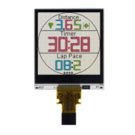
This TFT-LCD module is a reflective active matrix memory liquid crystal display module with CG silicone thin film
transistor. Module outline is indicated in fig 8-1.
2. Characteristics
・ Reflective panel of white and black with aspect ratio of 1:1
・ 1.3” screen has 96x 96 resolusion. (9216 pixels stripe array)
・ Display control by serial data signal communication.
・ Arbitrary line data renewable.
・ 1bit internal memory for data storage within the panel.
・ Thin, light-weight and compact module with monolithic technology.
・ Super low power consumption TFT panel.
3. Mechanical Specification
Table 3-1
Item Specification unit
Screen size 3.4 (1.3”)cm
Viewing Area 24.192(H)×24.192(V) mm
Dot configuration 96(H)× 96(V) Dot
Dot pitch 0.252 (H)×0.252 (V) mm
Pixel Array Stripe Array -
Outline Dimension
28.2(W)×32.34(H)×1.40 (D) mm
Mass 3.6(TYP)g
Surface Hardness 3HPencil hardness
(Note) Detail dimension and tolerance are shown in fig. 8-1
The FPC shape isn’t included in the outline dimension.

SPEC No.
LCY-12T09303B
MODEL No.
LS013B4DN02
PAGE
8
4. Input terminal names and functions
Table4-1
Terminal symbol I/O Function Remark
1 SCLK INPUT Serial clock signal
2 SI INPUT Serial data input signal
3 SCS INPUT Chip select signal
4 EXTCOMIN INPUT External COM inversion signal input (H: enable)
5 DISP INPUT Display ON/OFF signal 【Remark4-2】
6 VDDA POWER Power supply (Analog)
7 VDD POWER Power supply (Digital)
8 EXTMODE INPUT COM inversion select terminal 【Remark4-1】
9 VSS GND GND(Digital)
10 VSSA GND GND(Analog)
【Remark4-1】When it’s ”H”, EXTCOMIN signal is enable. And when it’s ”L” ,sirial input flag is enable.
“H”mode; connect the EXTMODE toVDD, ”L” mode; connect the EXTMODE to VSS.
【Remark4-2】The display ON/OFF signal is only for display. Data in the memory will be saved at the time of ON/OFF.
When it’s ”H”, data in the memory will display, when it’s ”L”, white color will diaplay and data in the memory will be
saved.
4-2)Recommended circuit;

SPEC No.
LCY-12T09303B
MODEL No.
LS013B4DN02
PAGE
9
5. Absolute Maximum Rating
Table5-1( GND=0V )
Item Symbol MIN. MAX. Unit Remark
Analog VDDA -0.3 +5.8 VPower
supply
voltage
Logic VDD -0.3 +5.8 V [Remark5-1]
Input signal voltage(high) VDD V [Remark5-2]
Input signal voltage(low) -0.3 V
Strage Temperature Tstg -30 +80 ℃[Remark5-3,4]
Operation Temperature
(at panel surface)
Topr1 -20 +70 ℃[Remark5-5]
[Remark5-1] Applies to EXTMODE.
[Remark5-2] Applies to SCLK, SI, SCS, DISP, EXTCOMIN.
[Remark5-3] Do not exceed this temperature in any parts of module.
[Remark5-4] Maximum wet bulb temperature is 57℃or lower. No condensation is allowed.
Cndensation will cause electeical leak and may cause the module to not meet this specification.
[Remark5-5] Operating temperature is the temperature that guarantees only for the operation.
For contrast, response time, and other display quality determination, use Ta=+25℃.

SPEC No.
LCY-12T09303B
MODEL No.
LS013B4DN02
PAGE
10
6. Electrical characteristics
6-1) TFT LCD panel drive
Table6-1Recommended operating Condition VSS(GND)=0V、Ta=+25℃
Item symbol MIN. TYP. MAX. Unit Remark
Analog VDDA
+4.8 +5.0 +5.5 VPower supply
Logic VDD
+4.8 +5.0 +5.5 V [Remark6-1]
Hi VIH
+2.70 +3.00 ※VDD VInput signal voltage
Lo VIL VSS VSS VSS+0.15 V
[Remark6-2]
Hi IOH - - TBD uA [Remark6-2]
VI=3V
Input leak current
Lo IOL - - TBD uA [Remark6-2]
VI=0V
※Can operate below VDD voltage, however, operation around 3V is recommended.
[Remark6-1] Applies to EXTMODE=”H”
[Remark6-2] Applies to SCLK, SI, SCS, DISP, EXTCOMIN.

SPEC No.
LCY-12T09303B
MODEL No.
LS013B4DN02
PAGE
11
6-2) Power supply sequence
①②
③※1④※1⑤⑥⑦
VDD/VDDA(5V)
GND GND
DISP
GND GND
EXTCOMIN
GND GND
SCS
GND
※2※2
GND
Others
GND
※2※2
GND
Normal operation
Normal operation
Normal operation
T1
Off sequenceNormal operation
T2 T3 T4 T5 T6 T7
On Sequence
※Refer to timing chart and AC timing characteristics for detail
※1 ③and ④may be opposite (however, TCOM polarity inversion will not occur even with EXTCOMIN between
DISP=”L”. Also, when DISP and EXTCOMIN are simultaneously started up, allow 30us or more before SCS
starts up (It may be less than 60us).
※2 Setting value for pixel memory initialization
SCS=Driving accordingly to clear pixel internal memory method (use all clear flag or write all screen white)
S1=M2 (all clear flag) = “H” or write white
SCLK: Normal Driving
[ON Sequence]
(1) 5V rise time (depends on IC)
(2) Pixel memory initialization T2: 1V or more Initialize with M2 (all clear flag) or write all screen white
(3) Release time for initialization of TCOM latch T3: 30us or more
Time required to release COM related latch circuit initialization which is initializing using DISP signals
(4) TCOM polarity initialization time T4: 30us or more
Time required initializing TCOM polarity accordingly to EXTCOMIN input
[Normal Operation]
Duration of normal driving
[Off Sequence]
(5) Pixel memory initialization time T5: 1V or more
(6) VA, VB, VCOM initialization time T6: 1V or more
(7) 5V falling time (Depends on IC)
[Remark] Precaustions at ehte time of power on and power off.
Remark 1)When power on , VDDand VDDA are same timem or VDD should be faster than the VDDA.
Remark 2) When power off, VDD and VDDA are same time or VDDA shoud be faster than the VDD.

SPEC No.
LCY-12T09303B
MODEL No.
LS013B4DN02
PAGE
12
6-3) Input signal characteristics
Table6-3-1 VDDA=+5.0V、VDD=+5.0V、GND=0V、Ta=25℃
Item Symbol MIN TYP MAX Unit Remark
Frame frequency fSCS 1 - 60 Hz
Clock frequency fSCLK 1 2 MHz
Vertical Interval tV 16.66 - 1000 ms
COM Frequency fCOM 0.5 - 30 Hz
Table 6-3-2 VDDA=+5.0V、VDD=+5.0V、GND=0V、Ta=25℃
Item Symbol MIN TYP MAX Unit Remark
SCS Rising time trSCS - - 50 ns
SCS Falling Time tfSCS - - 50 ns
68 - - usSCS High duration twSCSH
12 - - us
SCS Low duration twSCSL 1 - - us
SCS set up time tsSCS 3 - - us
SCS hold time thSCS 1 - - us
SI frequency fSI - 0.5 1 MHz
SI Rising time trSI - - 50 ns
SI Folling time tfSI - - 50 ns
SI set up time tsSI 120 - - ns
SI hold time thSI 125 - - ns
SCLK Rising time trSCLK - - 50 ns
SCLK Folling time tfSCLK - - 50 ns
SCLK High duration twSCLKH 200 450 - ns
SCLK Low duration twSCLKL 200 450 - ns
EXTCOMIN signal freequency fEXTCOMIN 1 60 Hz [Remark6-3]
EXTCOMIN signal rising time trEXTCOMIN - - 50 ns
EXTCOMIN signal folling time twEXTCOMIN - - 50 ns
EXTCOMIN signalHigh duration thlEXTCOMIN 1 us
DISP Rising time trDISP - - 50 ns
DISP Folling time tfDISP - - 50 ns
【Remark 6-3】EXTCOMIN frequency should be made lower than frame frequency.

SPEC No.
LCY-12T09303B
MODEL No.
LS013B4DN02
PAGE
13
10%
90%
10%
90%
10%
90%
10%
90%
10%
90%
50%
10%
90% 50% 50%
10%10%
50% 50% 50% 50%
twSCSH twSCSL
tfSCSthSCStrSCS tsSCS
trSI
tsSI thSI
tfSI
trSCLK tfSCLK
twSCLKH twSCLKL
SCS
SI
SCLK
10%
90%
10%
90%
trEXTCOMIN
50% 50% 50%
twEXTCOMINH
fEXTCOMIN
tfEXTCOMIN
10%
90%
10%
90%
trDISP tfDISP
EXTCOMIN
DISP
SCS, SI, SCLK signal
EXTCOMIN signal
DISP signal
※SCS,SI,SCLK、DISP、EXTCOMIN: 3V input voltage

SPEC No.
LCY-12T09303B
MODEL No.
LS013B4DN02
PAGE
14
6-4) Power consumption (Average)
Table6-4 Ta=25℃
Item Symbol MIN TYP MAX unit Remark
Condition1 15 uW [Remark6-4]
Condition2 30 uW [Remark6-4]
* Measurement Condition 1
Display mode (no display data update), Display pattern: Vertical stripe display
* Measurement Condition 2
Data update mode (with display data update: 1Hz)
Common inversion with VDD=5V、VDDA=5V、fSCLK=1MHz、fSCS=1Hz, Display pattern: Vertical stripe display
【Remark 6-4】This is value in steady condition, not the falue of peak power at the time of COM operation. Some
marging for power supply is recommended. We recommend capacitor for VDD and VDDA. (If VDD and
VDDA are on separate systems, we recommend capacitor for each.)

SPEC No.
LCY-12T09303B
MODEL No.
LS013B4DN02
PAGE
15
6-5) Input Signal Timing Chart
6-5-1 Data update mode (1 line)
Updates data of only one specified line. (M0=”H”、M2=”L”)
SCS
SI M0 M1 M2 DM
Y
DM
Y
DM
Y
DM
Y
DM
Y
AG0 AG1 AG2 AG3 AG4 AG5 AG6DM
Y
D1 D2 D3 D4 D93 D94 D95 D96 DUMMY DATA
(
don't care
)
SCLK
tsSI thSI
tsSCS
Data writing period
(96ck)
Data transfer period
(16ck)
Mode selection period
(3ck+5ckDMY)
twSCLKHtwSCLKL
twSCSH
Gate line address period
(7ck+1ckDMY)
thSCS
twSCSL
M0: Mode flag. Set for “H”. Data update mode (Memory internal data update)
When “L”, display mode (maintain memory internal data).
M1: Frame inversion flag.
When “H”, outputs VCOM=”H”, and when “L”, outputs VCOM=”L”.
When EXTMODE=”H”, it can be “H” or “L”.
M2: All clear flag.
Refer to 6-5-4) All Clear Mode to execute clear.
DUMMY DATA: Dummy data. It can be “H” or “L” (“L” is recommended.)
※Data write period
Data is being stored in 1st latch block of binary driver on panel.
※Data transfer period
Data written in 1st latch is being transferred (written) to pixel internal memory circuit.
※For gate line address setting, refer to 6-6) Input Signal and Display.
※M1: Frame inversion fl is enaled when EXTMODE=”L”.
※When SCS becomes “L”, M0 and M2 are cleared.

SPEC No.
LCY-12T09303B
MODEL No.
LS013B4DN02
PAGE
16
6-5-2 Data Update Mode (Multiple Lines)
Updates arbitrary multiple lines data. (M0=”H”、M2=”L”)
SCS
SI
DUMMY DATA(don't care)
SCLK
DU M M Y D AT A( don' t c ar e)
DUMMY DA T A ( do n 't c a r e)D95 DMYAG6AG5AG4AG0 AG1D96
AG3 DMYAG6AG5AG4 D94 D95 D1D1 D2 D3 DMYAG6AG5DMY DMY D2AG1D4 AG0D93 D96M0 M2 DMY DMYM1 DMY
D95 D96D2 D94D1
AG0 AG1 AG2
tsSI thSI
tsSCS
GL1
Data transfer period
(96ck)
GL2
Mode selection period
(3ck+5ckDMY)
GL(n)th line
Data writing period
(96ck)
Data transfer period
(16ck)
GL(n-1)th Line
thSCS
twSCLKHtwSCLKL
twSCSLtwSCSH
twSCSH
Gate line address period
(7ck+1ckDMY)
Data transfer period
(8ck(Dymmy)+7ck(address)+1ck(Dummy)=16ck)
Data transfer period
(8ck(Dummy)+7ck(address)+1ck(Dummy)=16ck)
M0: Mode flag. Set for “H”. Data update mode (Memory internal data update)
When “L”, display mode (maintain memory internal data).
M1: Frame inversion flag.
When “H”, outputs VCOM=”H”, and when “L”, outputs VCOM=”L”.
When EXTMODE=”H”, it can be “H” or “L”.
M2: All clear flag.
Refer to 6-5-4) All Clear Mode to execute clear.
DUMMY DATA: Dummy data. It can be “H” or “L” (“L” is recommended.)
※Data write period
Data is being stored in 1st latch block of binary driver on panel.
※Data transfer period
For example, during GL2nd line data transfer period, GL 2nd line address is latched and GL1st
line data is transferred from 1st latch to pixel internal memory circuit at the same time.
※For gate line address setting, refer to 6-6) Input Signal and Display.
※Input data continuously.
※M1: Frame inversion flag is enabled when EXTMODE=”L”.
※When SCS becomes “L”, M0 and M2 are cleared.

SPEC No.
LCY-12T09303B
MODEL No.
LS013B4DN02
PAGE
17
6-5-3 Display Mode
Maintains memory internal data (maintains current display). (M0=”L”、M2=”L”)
SCS
SI
DUMMY DATA(don't care) DU M M Y DA TA( don' t c are)
SCLK
M0 M1 M2M0 M1 M2
tsSI thSI
tsSCS
Mode selection
period
(3ck)
twSCSH
tV
thSCS
twSCSL
Data transfer period
(More than 13ck)
M0: Mode flag. Set for “H”. Data update mode (Memory internal data update)
When “L”, display mode (maintain memory internal data).
M1: Frame inversion flag.
When “H”, outputs VCOM=”H”, and when “L”, outputs VCOM=”L”.
When EXTMODE=”H”, it can be “H” or “L”.
M2: All clear flag.
Refer to 6-5-4) All Clear Mode to execute clear.
DUMMY DATA: Dummy data. It can be “H” or “L” (“L” is recommended.)
※M1: Frame inversion flag is enabled when EXTMODE=”L”
※When SCS becomes “L”, M0 and M2 are cleared.

SPEC No.
LCY-12T09303B
MODEL No.
LS013B4DN02
PAGE
18
6-5-4 All Clear Mode
Clears memory internal data and writes white. (M0=”L”、M2=”H”)
SCS
SI DUM MY DAT A( don' t car e) D UM M Y D ATA( don' t c ar e)
SCLK
M1 M2M0 M1 M2 M0
tsSI thSI
tsSCS
twSCSH
tV
thSCS
twSCSL
Mode selection
period
(3ck)
Data transfer period
(More than 13ck)
M0: Mode flag.
Set it “L”.
M1: Frame inversion flag.
When “H”, outputs VCOM=”H”, and when “L”, outputs VCOM=”L”.
When EXTMODE=”H”, it can be “H” or “L”.
M2: All clear flag.
Set it “H”
DUMMY DATA: Dummy data. It can be “H” or “L” (“L” is recommended.)
※M1: Frame inversion flag is enabled when EXTMODE=”L”.
※When SCS becomes “L”, M0 and M2 are cleared.

SPEC No.
LCY-12T09303B
MODEL No.
LS013B4DN02
PAGE
19
6-5-5 COM Inversion
There are two types of inputs, COM signal serial input (EXTMODE=”L”) and external COM signal input (EXTMODE=”H”).
EXTMODE=“L”
SCS
SI
COM
M0 M1 M2 M0 M2M1 M2 M0 M1
fCOM
※2※2
※1※1※1
M1:LC polarity inversion flag: If M1is "H" then VCOM="H" is output. If M1 is "L" then VCOM="L" is output.
※1:LC inversion has been changed by M1 flag statement.
※2:The periods of plus polarity and minus polarity should be same length as much as possible.
EXTMODE=“H”
SCS
EXTCOMIN
COMZ
COM
fCOM
※2※2
※1※1※1
fEXTCOMIN twEXTCOMIN
※1:LC inversion polarity has been set by the rising timing of EXTCOMIN in internal circuit block as COMZ signal,
※2:The period of EXTCOMIN should be constant.
Table of contents
Other Sharp Control Unit manuals

Sharp
Sharp ND-158E1F User manual

Sharp
Sharp NU-JC365B User manual

Sharp
Sharp NQ-R258H User manual

Sharp
Sharp NB-JD580 User manual

Sharp
Sharp NU-AK300 User manual

Sharp
Sharp ND-AH330 User manual

Sharp
Sharp NU-JC410 User manual

Sharp
Sharp NU-JC415B User manual

Sharp
Sharp NB-JD575 User manual

Sharp
Sharp NU-JC375 User manual

Sharp
Sharp PN-ZB03PC User manual

Sharp
Sharp NU-JC400B User manual

Sharp
Sharp LS013B7DH01 User manual

Sharp
Sharp ND-AK270 User manual

Sharp
Sharp LQ197V3DZ81 Application guide

Sharp
Sharp ND-RK270 User manual

Sharp
Sharp LS013B7DH01 User manual

Sharp
Sharp ND-123UJF Guide
Sharp
Sharp MX-PEX1 User manual

Sharp
Sharp LS013B7DH07 User manual