– 7 –
CD-K1861V
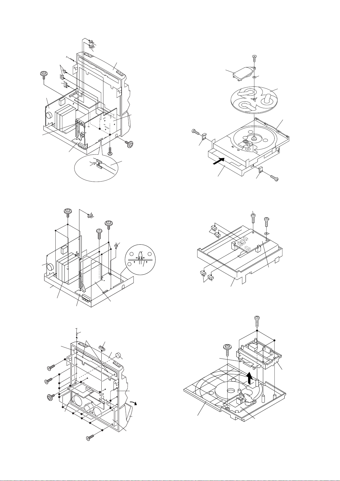
DISASSEMBLY
Caution on Disassembly
Follow the below-mentioned notes when disassembling
the unit and reassembling it, to keep it safe and ensure
excellent performance:
1. Take cassette tape and compact disc out of the unit.
2. Be sure to remove the power supply plug from the wall
outlet before starting to disassemble the unit.
3.Take offnylon bands or wire holderswhere theyneed to
beremovedwhendisassemblingtheunit.Afterservicing
theunit, besure to rearrange the leadswhere theywere
before disassembling.
4. Take sufficient care on static electricity of integrated
circuits and other circuits when servicing.
Figure 7-2
Figure 7-3
CD-K1861V
Figure 7-1
LOCK
LEVER
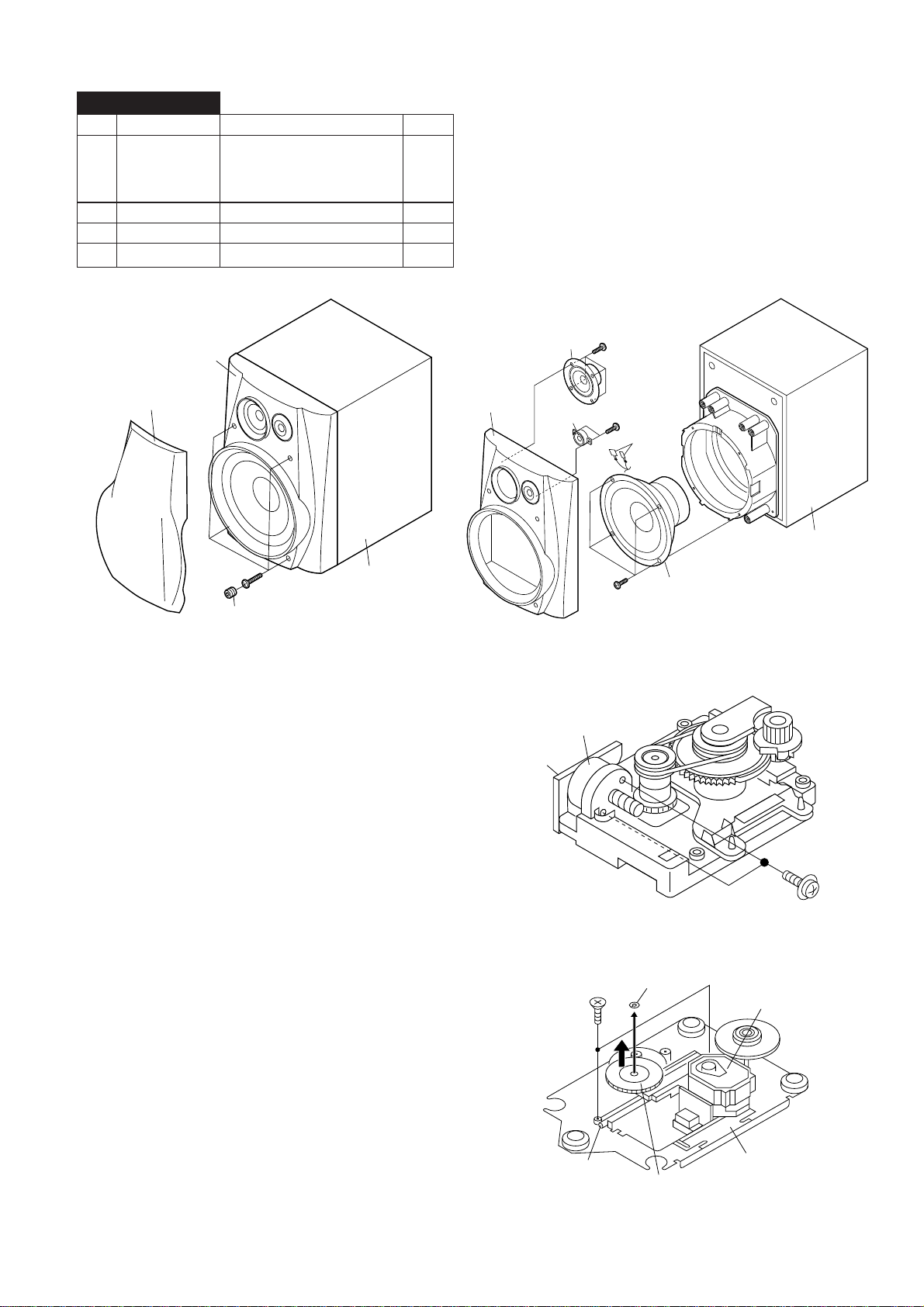
1 Top Cabinet 1. Screw ..................... (A1) x4 7-1
2 Side Panel 1. Screw ..................... (B1) x8 7-1
(Left/right)
3 CD Player Unit/ 1. Turn on the power supply, 7-2
CD Tray Cover open the disc tray, take out
the CD cover, and close.
(Note 1)
2. Screw ..................... (C1) x1
3. Hook....................... (C2) x3
4. Hook....................... (C3) x2
5. Socket .................... (C4) x5
4 Rear Panel 1. Screw ..................... (D1) x9 7-2,
(with Digital 8-1
Output PWB)
5 Main PWB/ 1. Screw ..................... (E1) x1 8-1
Tuner PWB 2. Socket .................... (E2) x4
3. Flat Cable............... (E3) x1
4. Tip .......................... (E4) x1
6 Front Panel 1. Screw ..................... (F1) x3 8-1
2. Socket .................... (F2) x1
7 Power Amp. PWB 1. Screw ..................... (G1) x7 8-2
2. Socket .................... (G2) x2
3. PWB Holder ........... (G3) x1
8
Power Supply PWB
1. Screw ..................... (H1) x4 8-2
9
Karaoke PWB
1. Screw ..................... (J1) x2 8-3
2. Tip .......................... (J2) x1
10 Display PWB/ 1. Screw ..................... (K1) x13 8-3
Switch PWB 2. Socket .................... (K2) x1
3. Hook....................... (K3) x2
4. Buttom.................... (K4) x1
11 Tape Mechanism 1. Open the cassette holder. 8-3
2. Screw...................... (L1) x6
12 Turntable 1. Screw ..................... (M1) x1 8-4
2. Cover ..................... (M2) x1
13 Disc Tray 1. Screw ..................... (N1) x2 8-4
2. Guide ..................... (N2) x2
14 CD Video PWB 1. Screw ..................... (P1) x2 8-5
(Note 2) 2. Socket .................... (P2) x4
15 CD Changer 1. Screw ..................... (Q1) x4 8-6
Mechanism
16 CD Mechanism 1. Screw ..................... (R1) x1 8-6
STEP REMOVAL PROCEDURE FIGURE
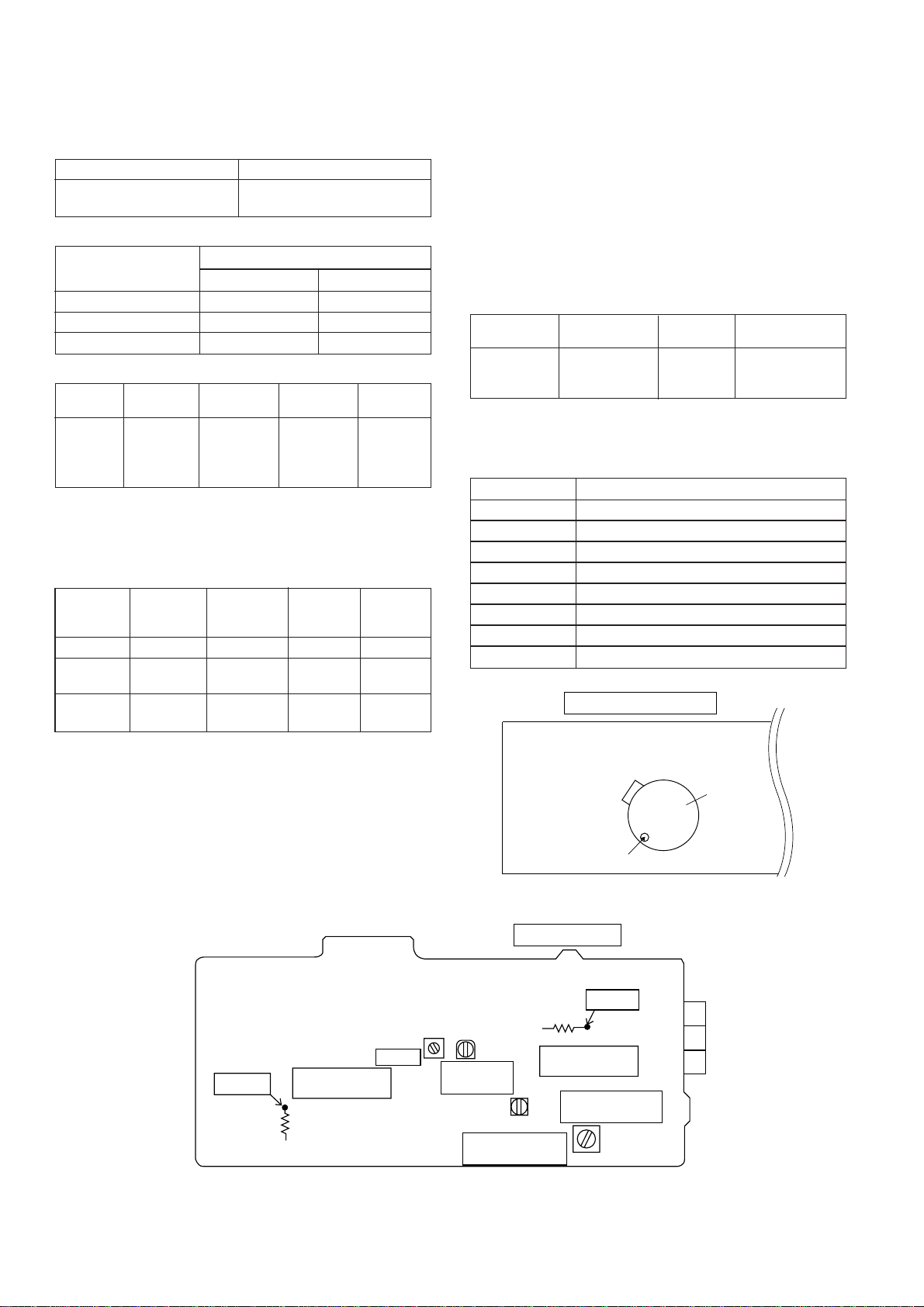
Note 1:
How to open the changer manually. (Fig. 7-3)
1. Change, turn fully the lock lever in the arrow direction
throughtheholeontheloadingchassisbottominthisstate.
After that, push forward the CD player base.
CD-K1861V
Note 2:
1.After removing theconnector forthe optical pickupfrom the
connector, wrap the conductive aluminium foil around the
front end of connector to protect the optical pickup from
electrostatic damage.
Top Cabinet Front Panel
(A1) x2
ø3 x12mm
(A1) x2
ø3 x12mm
Side Panel
(Left)
Side Panel
(Right)
(B1) x2
ø3 x10mm
(B1) x2
ø3 x10mm
(B1) x4
ø3 x10mm
Back Board
(D1) x1
ø3 x10mm
CD Tray Cover
CD Player
Unit
CD Video
PWB
Hook
(C2) x3
(C3) x1
(C4) x4
(C4) x1
1
1
2
Pull
(C3) x1
Rear Panel
(C1) x1
ø3 x10mm
(D1) x4
ø3 x10mm
(D1) x3
ø3 x6mm
Front Panel
Main PWB


 User manual")