Sharp XL-T200H User manual

– 1 –
XL-T200H
CONTENTS Page
SAFETY PRECAUTION FOR SERVICE MANUAL .......................................................................................................... 2
IMPORTANT SERVICE NOTES (FOR U.K. ONLY) ......................................................................................................... 2
SPECIFICATIONS ............................................................................................................................................................ 3
NAMES OF PARTS .......................................................................................................................................................... 4
DISASSEMBLY................................................................................................................................................................. 6
REMOVING AND REINSTALLING THE MAIN PARTS.................................................................................................... 8
NOTES ON SCHEMATIC DIAGRAM ............................................................................................................................. 10
TYPES OF TRANSISTOR AND LED.............................................................................................................................. 10
BLOCK DIAGRAM .......................................................................................................................................................... 11
SCHEMATIC DIAGRAM ................................................................................................................................................. 14
WIRING SIDE OF P.W.BOARD...................................................................................................................................... 24
WAVEFORMS OF CD CIRCUIT..................................................................................................................................... 28
TROUBLESHOOTING.................................................................................................................................................... 29
PARTS GUIDE/EXPLODED VIEW
PACKING METHOD (FOR U.K. ONLY)
SERVICE MANUAL
SHARP CORPORATION
No. S5235XLT200H/
• In the interests of user-safety the set should be restored to its original
condition and only parts identical to those specified should be used.
This document has been published to be used
for after sales service only.
The contents are subject to change without notice.
XL-T200H Compact Audio System consisting of XL-T200H
(main unit) and CP-XLT200H (speaker system).
COMPACT AUDIO SYSTEM
MODEL XL-T200H
(Except for U.K.)
ThisServiceManualisfortheXL-T200H,whichisaminormodificationmodeloftheXL-T300H.ThisServiceManual,therefore,describes
only the changed points from the Service Manual. Please refer to the XL-T300H Service Manual (S4225XLT300H/) together with this
Service Manual.

XL-T200H
– 2 –
Beforereturningtheunittothecustomeraftercompletionofa
repairoradjustmentit isnecessary forthe followingwithstand
voltage test to be applied to ensure the unit is safe for the
customer to use.
Setting of Withstanding Voltage Tester and set.
Set name set value
Withstanding Voltage Tester
Test voltage 4,240 VPEAK
3,000 VRMS
Set time 6 secs
Set current(Cutoff current) 4 mA
Unit
Judgment
OK: The “GOOD” lamp lights.
NG: The “NG” lamp lights and the buzzor sounds.
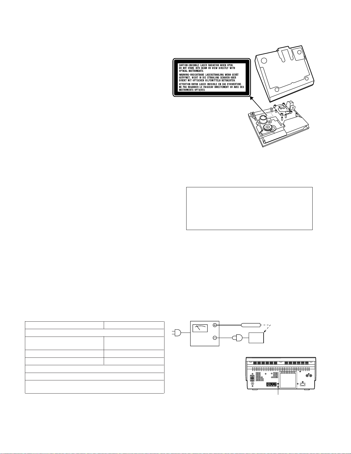
This product is classified as a CLASS 1 LASER PRODUCT.
Precaution to be taken when replacing and servicing the
Laser Pickup.
TheAEL(AccessibleEmissionLevel)of LaserPowerOutputis
lessthanClass1butthelasercomponentiscapableofemitting
radiationexceedingthelimitforClass1.Thereforeitisimportant
thatthefollowingprecautionsmustbeobservedduringservicing
to protect your eyes against exposure to the Laser beam.
(1) When the cabinet has been removed, the power is turned
on without a compact disc, and the Pickup is on a position
outerthanthelead-inposition,theLaserwilllightforseveral
seconds to detect a disc. Do not look into the Pickup Lens.
(2) The Laser Power Output of the Pickup inside the unit and
replacementservicepartshavealreadybeenadjustedprior
to shipping.
(3) No adjustment to the Laser Power should be attempted
when replacing or servicing the Pickup.
(4) Under no circumstances look directly into the Pickup Lens
at any time.
(5)CAUTION-Useof controlsor adjustments,orperformance
of procedures other than those specified herein may result
in hazardous radiation exposure.
SAFETY PRECAUTION FOR SERVICE MANUAL
IMPORTANT SERVICE NOTES (FOR U.K. ONLY)
PROBE
AC OUT UNIT
SHORT-CIRCUT
AC POWER
SUPPLY CORD
WITHSTANDING
VOLTAGE TESTER
Screw
Laser Diode Properties
Material: GaAIAs
Wavelength: 780 nm
Emission Duration: continuous
Laser Output: max. 0.6 mW
VAROITUS! LAITTEEN KÄYTTÄMINEN MUULLA KUIN TÄSSÄ
KÄYTTÖOHJEESSA MAINITULLA TAVALLA SAATTAA
ALTISTAA KÄYTTÄJÄN TURVALLISUUSLUOKAN 1
YLITTÄVÄLLE NÄKYMÄTTÖMÄLLE LASERSÄTEILYLLE.
VARNING - OM APPARATEN ANVÄNDS PÅ ANNAT SÄTT ÄN
I DENNA BRUKSANVISNING SPECIFICERAS. KAN
ANVÄNDAREN UTSÄTTAS FÖR OSYNLIG LASER-
STRÅLNING, SOM ÖVERSKRIDER GRÄNSEN FÖR
LASERKLASS 1.
ADVERSEL-SYNLIG OG USYNLIG LASERSTRÅLING VED ÅBNING.
SE IKKE IND I STRÅLEN-HELLER IKKE MED OPTISKE INSTRUMENTER.
VARO!AVATTAESSAOLETALTTIINA NÄKYVÄLLE JANÄKYMÄTTÖMÄLLE
LASERSÄTEILYLLE ÄLÄ TUIJOTA SÄTEESEEN ÄLÄKÄ KATSO SITÄ
OPTISEN LAITTE EN LÄPI.
VARNING-SYNLIG OCH OSYNLIG LASERSTRÅLNING NÄR DENNA
DELÄR ÖPPNAD. STIRRAEJ IN I STRÅLEN OCH BETRAKTA EJ
STRÅLEN GENOM OPTISKT INSTRUMENT.

– 3 –
XL-T200H
SPECIFICATIONS
Specifications for this model are subject to change without
prior notice.
FOR A COMPLETE DESCRIPTION OF THE OPERATION OF THIS UNIT, PLEASE REFER
TO THE OPERATION MANUAL.
■General
■Amplifier
Power source AC 230 V, 50 Hz
Power consump-
tion Power on: 26 W
Power stand-by: 0.6 W
Dimensions Width: 290 mm (11-7/16")
Height: 130 mm (5-1/8")
Depth: 260 mm (10-1/4")
Weight 2.8 kg (6.2 lbs.)
Output power PMPO: 30 W (total)
MPO: 15 W (7.5 W + 7.5 W) (DIN 45 324)
RMS: 10 W (5 W + 5 W) (DIN 45 324)
Output terminals Speakers: 4 ohms
Headphones: 16 - 50 ohms (recommended:
32 ohms)
Input terminals Video/Auxiliary (audio signal): 500 mV/47
kohms
■CD player
■Tuner
■Cassette deck
■Speaker
Type Compact disc player
Signal readout Non-contact, 3-beam semiconductor laser
pickup
D/A converter 1-bit D/A converter
Frequency re-
sponse 20 - 20,000 Hz
Dynamic range 90 dB (1 kHz)
Frequency range FM: 87.5 - 108 MHz
AM: 522 - 1,620 kHz
Frequency re-
sponse 50-14,000 Hz (Normal tape)
Signal/noise ratio 50 dB (recording/playback)
Wow and flutter 0.3 % (DIN 45 511)
Tweeter 2-way type speaker system
Tweeter
10 cm (4") Woofer
Maximum input
power 10 W
Rated input power 5 W
Impedance 4 ohms
Dimensions Width: 146 mm (5-3/4")
Height: 267 mm (10-9/16")
Depth: 186 mm (7-3/8")
Weight 1.5 kg (3.3 lbs.)/each

XL-T200H
– 4 –
NAMES OF PARTS
■Front panel
1.CD/Cassette Compartment
2.Function Selector Button
3.Bass/Treble Selector Button
4.Memory/Set Button
5.Tape Record Pause Button
6.Volume Up and Down Buttons
7.CD or Tape Open/Close Button
8.CD Track Down or Fast Reverse, Tape Rewind,
Tuner Preset Down Button
9.CD Track Up or Fast Forward, Tape Fast Forward,
Tuner Preset Up Button
10.CD or Tape Stop, Tuning Down Button
11.CD Play or Pause, Tape Play, Tuning Up Button
12.On/Stand-by Button
■Display
1.Timer Play Indicator
2.Tape Record Indicator
3.Sleep Indicator
4.CD Random Play Indicator
5.Memory Indicator
6.RDS Indicator
7.Traffic Programme Indicator
8.Traffic Announcement Indicator
9.FM Stereo Mode Indicator
10.CD Play Indicator
11.CD Repeat Play Indicator
12.FM Stereo Receiving Indicator
13456789
11
10 12
2
1
23 4567
8 9 10 11 12
■Rear panel
1.Speaker Terminals
2.Headphone Socket
3.AM Aerial Terminal
4.Aerial Earth Terminal
5.FM 75 Ohms Aerial Socket
6.Video/Auxiliary (Audio Signal) Input Sockets
7.AC Power Input Socket
■Speaker system
1.Tweeter
2.Woofer
3.Bass Reflex Duct
4.Speaker Wire
Speaker grilles are removable:
Placing the speaker system:
There is no distinction between the right and the left speakers.
3
2
1
4
5
6
7
4
1
2
3
Make sure nothing comes into contact with the
speaker diaphragms when you remove the
speaker grilles.
Left speaker Right speaker

– 5 –
XL-T200H
■Remote control
1.Remote Control Transmitter
2.On/Stand-by Button
3.CD Button
4.Tuner and Band Selector Button
5.Timer Button
6.Clock Button
7.Memory Button
8.Dimmer Button
9.Volume Up and Down Buttons
10.Video/Auxiliary Button
11.Tape Button
12.Clear Button
13.Sleep Button
14.Random/Repeat Button
15.CD or Tape Open/Close Button
16.Tape Record Pause Button
17.Tuner Preset Up Button
18.CD Track Down Button
19.CD Fast Reverse, Tuning Down,
Tape Rewind Button
20.CD or Tape Play Button
21.CD Track Up Button
22.CD Fast Forward, Tuning Up,
Tape Fast Forward Button
23.CD Pause Button
24.CD or Tape Stop Button
25.Tuner Preset Down Button
26.Bass Up and Down Buttons
27.Treble Up and Down Buttons
28.RDS Programme Type/
Traffic Information Search Button
29.RDS ASPM (Auto Station Programme Memory) Button
30.RDS Dis
p
la
y
Mode Selector Button
Buttons with " " mark in the illustration can be operated on the re-
mote control only.
1
2
3
4
5
6
7
8
9
10
11
12
13
14
15
17 21
22
23
18
19
20
24 25
26 27
28 29 30
16

XL-T200H
– 6 –
1 Top Cabinet 1. Screw ..................(A1) x6 6-1,2
2. Hook ....................(A2) x4 6-2
3. Socket .................(A3) x9
4. Flat Cable............(A4) x1
2 Bottom Cabinet 1. Screw ................(B1) x11 6-1,3
/Chassis 2. Hook ....................(B2) x3 6-3
3 Tuner PWB 1. Screw ................. (C1) x2 7-1
2. Socket ................ (C2) x1
4 Terminal PWB 1. Screw ................. (D1) x2 7-1
2. Socket ................ (D2) x1
5 Main PWB 1. Screw ..................(E1) x8 7-1
2. Socket .................(E2) x2
6 CD Mechanism 1. Screw .................. (F1) x4 7-2
7 Tape Mechanism 1. Screw ................. (G1) x4 7-2
8 Gear Box 1. Screw ................. (H1) x3 7-3
2. Socket ................ (H2) x1
9 Switch PWB 1. Screw .................. (J1) x1 7-3
10
LED PWB/Holder PWB
1. Screw ..................(K1) x1 7-3
11 Display PWB 1. Screw .................. (L1) x7 7-3
/Switch PWB 2. Hook .................... (L2) x4
DISASSEMBLY
STEP REMOVAL PROCEDURE FIGURE
Note:
After removing the connector for the optical pickup from the
connector, wrap the conductive aluminium foil around the
front end of connector remove to protect the optical pickup
from electrostatic damage.
Caution on Disassembly
Follow the below-mentioned notes when disassembling
the unit and reassembling it, to keep it safe and ensure
excellent performance:
1. Take compact disc out of the unit.
2. Be sure to remove the power supply plug from the wall
outlet before starting to disassemble the unit.
3.Takeoffnylonbandsorwire holders where they need to
beremovedwhendisassemblingtheunit.Afterservicing
theunit,besuretorearrangetheleadswheretheywere
before disassembling.
4. Take sufficient care on static electricity of integrated
circuits and other circuits when servicing.
Bottom Cabinet
Top Cabinet
(A1) x3
ø3 x10mm
(B1) x2
ø3 x10mm
(B1) x1
ø3 x10mm
(B1) x3
ø3 x10mm
Figure 6-1
Figure 6-2
Figure 6-3
Hook
Up Slide
Top Cabinet
Bottom Cabinet
Bottom Cabinet
Top Cabinet
CD Mechanism
Tape
Mechanism
(A1) x3
ø2.5 x12mm
Hook
(A2) x2
(A3) x4
(A4) x1
(A3) x3
Hook
(A2) x2 (A3) x2
Bottom
Cabinet
Chassis
Bottom Cabinet
Main PWB
Pull
Main PWB
(B1) x5
ø3 x8mm
Hook
(B2) x3

– 7 –
XL-T200H
Figure 7-1
Chassis
(E1) x3
ø3 x10mm
(E1) x3
ø3 x10mm
(D1) x1
ø3 x10mm
(E1) x1
ø3 x10mm
(D1) x1
ø3 x8mm (C1) x1
ø3 x8mm
(C2) x1
(C1) x1
ø3 x12mm
(E1) x1
ø3 x14mm
(E2) x2
(D2) x1
Main PWB Tuner PWB
Terminal
PWB
Figure 7-3
Top Cabinet
CD
Mechanism
CNW909
Tape
Mechanism
(F1) x4
ø2.5 x10mm
(G1) x4
ø3 x10mm
Holder PWB
Hook
(L2) x4
Holder PWB
Top Panel
(L1) x3
ø2.5 x10mm
(K1) x1
ø2.5 x10mm (H2) x1
(L1) x4
ø2.5 x8mm
(J1) x1
ø2.5 x8mm
(H1) x2
ø2.5 x10mm
(H1) x1
ø2.5 x10mm
Switch PWB
LED PWB
Switch PWB Gear Box
Display PWB
( A3 ) x4
ø3.5 x12mm
Tweeter
Net Frame
( A1 ) x1
Front Panel
( A2 ) x1
Woofer
Screwdriver
Figure 7-2
Figure 7-4
1 Speaker 1. Net Frame ........... (A1) x1 7-4
2. Front Panel ......... (A2) x1
3. Screw .................. (A3) x4
STEP REMOVAL PROCEDURE FIGURE

XL-T200H
– 8 –
TAPE MECHANISM SECTION
Perform steps 1 and 7 of the disassembly method to remove
the tape mechanism. (See page 6,7.)
How to remove the record / playback and erase
heads (See Fig. 8-1.)
1. Remove the screws (A1) x 2 pcs., to remove the erase
head.
2. Remove the screws (A2) x 2 pcs., to remove the record/
playback head.
Note:
After replacing the heads and performing the azimuth
adjustment, be sure to apply screwlock.
How to remove the pinch roller (See Fig. 8-2.)
1. Carefully bend the pinch roller pawl in the direction of the
arrow <A>, and remove the pinch roller (B1) x 1 pc.,
upwards.
How to remove the belts (See Fig. 8-3.)
1. Remove the main belt (C1) x 1 pc., from the motor pulley.
2. Remove the FF/REW belt (C2) x 1 pc., from the REW/FF
roller.
3. Put on the belts in the reverse order of removal.
Note:
Whenputtingonthe belt,ascertain thatthe beltisnottwisted,
and clean it.
How to remove the motor
(See Figs. 8-4.)
1. Remove the mainbelt.
2. Remove the screws (D1) x 2 pcs., to remove the motor
bracket.
3. Remove the screws (D2) x 3 pcs., to remove the motor.
Note:
Whenmountingthemotor,payattentiontothemotormounting
angle
<A>
Pinch Roller
(B1)x1 Pinch Roller
Pawl
REMOVING AND REINSTALLING THE MAIN PARTS
Main Belt
(C1)x1
FF/REW Belt
(C2)x1
REW/FF
Clutch
Motor
Erase Head
Record/
Playback Head
(A1)x2
ø2x8mm
(A2)x1
ø2x3mm
(A2)x1
ø2x7mm
(D1)x1
ø2x4mm
(D2)x3
Special
Screw
Motor
Bracket
Motor
Motor
(D1)x1
ø2x4mm
Figure 8-1
Figure 8-2
Figure 8-3
Figure 8-4
How to remove the flywheel (See Fig. 8-5.)
1. Remove the belt.
2.Removethestopwasher(E1)x1pc.,withasmallprecision
screwdriver to extract the flywheel from the capstan metal.
Note:
When the stop washer is deformed or damaged, replace it
with a new one.
How to reinstall the parts
Installeachpart in the reverse order oftheremovalwith care.
Stop
Washer Driver
(E1)x1
Stop Washer
Mechanism
Chassis
Washerx2
Flywheel
Figure 8-5

– 9 –
XL-T200H
How to remove the tape mechanism PWB
(See Fig. 9-1.)
1. Remove the screws (F1) x 1 pc., to remove the tape
mechanism PWB.
2. Remove the screws (F2) x 1 pc.
3. Remove the solder joints (F3) x 2 pcs., to remove the tape
mechanism PWB.
Tape
Mechanism
PWB Tape
Mechanism
PWB
(F3)x2
Solder
Joint
(F2)x1
ø2x8mm
(F1)x1
ø2x3mm
Figure 9-1
Figure 9-2
How to remove the CD lid (See Fig. 9-2.)
Perform steps 1 and 8 of the disassembly method to remove
the gear box.(See page 6,7)
1. Remove the screws (A1) x 2 pcs., to remove the CD lid
motor.
2.Removethehooks(A2)x3pcs.,toremovethewormwheel.
Caution:
Be careful so that the gear is not damaged.
(The damage gear emits noise during searching.)
(A1) x2
ø2 x5mm
Hook
(A2) x3
CD Lid Motor
Figure 9-3
CD MECHANISM SECTION (See Fig. 9-3.)
Perform steps 1 and 6 of the disassembly method to remove
the CD mechanism.(See page 6,7)
1. Remove the mechanism cover, paying attention to the
pawls (A1)x 4 pcs.
2. Remove the screws (A2) x 2 pcs., to remove the shaft (A3)
x 1 pc.
3. Remove the stop washer (A4) x 1 pc., to remove the gear
(A5) x 1 pc.
4. Remove the pickup unit.
Note:
After removing the connector for the optical pickup from the
connector, wrap the conductive aluminium foil around the
front end of connector remove to protect the optical pickup
from electrostatic damage.
Pickup unit
(A2) x2
ø2.6 x6mm
(A1) x4
CD Mechanism
Shaft
(A3) x1
Gear
(A5) x1
Stop Washer
(A4) x1
Mechanism Cover

XL-T200H
– 10 –
SW702 PICKUP IN ON—OFF
SW709 ON/STAND-BY ON—OFF
SW710 CD LID OPEN/CLOSE ON—OFF
SW711 VOLUME DOWN ON—OFF
SW712 VOLUME UP ON—OFF
SW721 FUNCTION ON—OFF
SW722 REW/PRESET DOWN ON—OFF
SW723 FF/PRESET UP ON—OFF
•The indicated voltage in each section is the one measured
by Digital Multimeter between such a section and the chas-
sis with no signal given.
1. In the tuner section,
( ) : AM mode
: FM stereo mode
2. In the CD section, the CD is stopped.
•Parts marked with “ ” ( ) are important for
maintaining the safety of the set. Be sure to replace these
parts with specified ones for maintaining the safety and
performance of the set.
NOTES ON SCHEMATIC DIAGRAM
•Resistor:
To differentiate the units of resistors, such symbol as K and
M are used: the symbol K means 1000 ohm and the symbol
M means 1000 kohm and the resistor without any symbol is
ohm-type resistor. Besides, the one with “Fusible” is a fuse
type.
•Capacitor:
To indicate the unit of capacitor, a symbol P is used: this
symbol P means micro-micro-farad and the unit of the
capacitor without such a symbol is microfarad. As to
electrolyticcapacitor,theexpression“capacitance/withstand
voltage” is used.
(CH), (TH), (RH), (UJ): Temperature compensation
(ML): Mylar type
(P.P.): Polypropylene type
•Schematic diagram and Wiring Side of P.W.Board for this
model are subject to change for improvement without prior
notice.
REF. NO DESCRIPTION POSITION POSITIONREF. NO DESCRIPTION
SW724 BASS/TREBLE ON—OFF
SW725 CD STOP/CLEAR/TUNING DOWN ON—OFF
SW726 MEMORY/SET ON—OFF
SW727 CD PLAY/PAUSE/TUNING UP ON—OFF
SW728 REC/PAUSE ON—OFF
SW802 CD LID ON—OFF
SW901 FOOL PROOF ON—OFF
SW902 CAM ON—OFF
ECB
(S)(G)(D)
FRONT
VIEW
FRONT
VIEW
BCE
FRONT
VIEW
2SB562 C
2SC380 O
2SC2001 K
KRA102 M
KRC102 M
KRC104 M
KRC107 M
KTA1266 GR
KTC3199 GR
KTC3200 GR 2SD2012 Y AUY3335
SLI343YC SVC348S
1 2 3
(1) (2) (3)
Figure 10 TYPES OF TRANSISTOR AND LED

– 11 –
XL-T200H
Figure 11 BLOCK DIAGRAM (1/3)
ANTENNA
TERMINAL
AM Band
Coverage fL
FM MUTE
LEVEL
AM IFFM IF
FM IF
FM IF AM IF
AM Band
Tracking fL
VD301
SVC348S
FM IF DET./
FM MPX./AM IF
IC303
LA1832S
+5V
+5V
VT
+5V
+5V
+B
+B
+B
4.332MHz
X521
+B
FM +B
+5V
FM +B
+5V
T302
T306
T351
CF301 CF302 CF352
CF351
L354
LOW PASS
FILTER SWITCHING
Q301
L341
BALUN
VR351
X352
4.5MHz
VOLTAGE
REGULATOR
AM
GND
FM
75ohms
SO301
VSM
AM RF
OUT
OUT
OUT
OUT
IN
IN
CUT
AM LOW
FM/AM
MPX VCO
MPX IN
MO/ST
L-CH
R-CH
FM AFC
AM OSC
AM OSC
(AM/FM)
PHASE
PHASE
IF OUT
VCC
FM DET
STEREO
SD
GND
AM IF
REG
AM MIX
OUT
IN
IN
FM IF
23 22 21 20 19 18 17 16 15 1424 13
121110987654321
PLL(TUNER)
111098765431
PD
IF IN
AM IN
FM IN
VDD
AIN
AOUT
VSS
X OUT
22 21 20 19 18 17 16 15 14 13 12
FM
FM
MUTE
CE
DI
CL
DO
MO/ST
IF REQ
X IN
IC302
LC72131
87654321
FE301
FM FRONT END
TP301
456kHz
X351
Q351
Q521
Q360
ZD351
TUNER PWB
16 15 14 13 12 11 10 9
1 2 3 4 5 6 7 8
14
13
12
11
10
9
8
7
6
5
4
3
2
1
RDS CLK
RDS DATA
VSM
SD
FM ST
DO
CL
CE
DI
A_12V
D_GND
TUN_L
TUN_R
A_GND
TO
MAIN PWB
LC72723M
RDS
CNS301
IC521
SWITCHING
RESET
SWITCHING
SWITCHING
Q701 Q702
Q703
COM0
COM3
SEG0
SEG33
REMOCON
P–CONT
VDD
32.768kHz
8MHz
38541
1
100
67
66
65
64
63
62
61
60
59
58
33
57
56
54
53
42
52
41
21
55
39 48 49 5032
47
TAPE SW
22
8
4
LCD701
FL DISPLAY
TO
MAIN PWB
REMOTE
SENSOR
RX701
RESET
23
VSM
VLC1
VLC2
VLC3
7
6
5
MMOD
VREF
VREF+
VSS
15
24
14
11
SYS_STOP
POWER
3837
13
12
10
9
X701
X702
OSC1
OSC2
XO
XI
CLID_SW
SW711,712
SW721~728
SW709
SW710
KEY1
KEY2
18
17
16
SYSTEM MICROCOMPUTER/
FL DRIVER
IC701
IX0045SJ
DATA
ST
SD
51
B-LIGHT
DI
CL
DO
CE
28272625
REC
BIAS
RUN PLS
SOL
MOT
B-CAN
35 3634313029
SURR
P-MUTE
P-STB
CD+B
46454443
CLE
40
DISPLAY PWB
Q708
Q707 Q709
Q706
GND
LED701
LED PWB
TO
MAIN PWB
TO
MAIN PWB TO
MAIN PWB TO
MAIN PWB
Q806
Q804
Q807
LED702
LED703
CDLID
MOTORDRIVER
M-GND
P-STB
M–12V
3
2
1
3
2
1
3
2
1
3
2
1
2
1
USWD5.6V
P_CONT
D_GND
12
11
10
9
8
7
6
5
4
3
12
11
10
9
8
7
6
5
4
3
2
1
CLE
DATA
VSM
D_GND
P_MUTE
CD+B
DI
CE
CL
DO
STEREO
SD
B-CAN
BLAS
U_CON5V
TAPE-SW
SOL
MOT
REC
RUN-PLS
1
2
1
2
3
4
5
6
7
8
1
2
3
4
5
6
7
8
SWITCH
PWB
CD LID
10
9
8
7
6
5
4
3
2
1
10
9
8
7
6
5
4
3
2
1
CD-RW
PU-IN
BUS0
BUS1
BUS2
BUS3
BUCK
CCE
CD-RES
CD-STB
GVSW
PU-IN
BUS0
DIMMER
LIGHT
CLID_UP
CLID_DW
AMP_DET
FAN_DET
FAN_CONT
PROTECT
SP_RLY
BUS1
BUS2
BUS3
BUCK
CCE
CD-RES
CD-STB
123 56789
LED PWB
M
CDLID
OPEN/CLOSE
TA7291S
CNW705
CNW701
CNW751
CNW702
CNW703
SW802
CNW704
IC804
LED801
M801(243-6)

XL-T200H
– 12 –
Figure 12 BLOCK DIAGRAM (2/3)
CD_L
CD_R
1
RDS CLK
TAPE
SOLENOID
–
+
FOOL
CAM
MOTOR
1
2
3
4
5
7
6
1
2
3
4
5
7
6
M
R-CH
L-CH
ERASE
HEAD
HEAD
RECORD/PLAY Q101-Q104
8
7
6
5
3
2
1
9
4
8
7
6
5
3
2
1
9
4
1
2 1
2
CNW101 CNP101
PHOTO
INTERRUPTER
10
9
8
5
2
9
8
7
6
5
4
3
2
1
11 6
3
4 1
HEAD SELECTOR
REC./P.B.
EQUALISER
AMP.
7 12
10
9
8
7
6
5
4
3
2
1 CD_RW
PU_IN
BUS0
BUS1
BUS2
BUS3
BUCK
CCE
CD_RES
CD_STB
1 2 3 4 5 6 7 8
Q80
Q802
GVSW
FEO
FEN
VRO
RFRP
RFIS
RFGO
RFGC
AGCI
RFO
RFN
GND
RFDC
TEO
TEN
TEBC
SEL
LDO
MDI
TN1
TPI
FPI
FNI
VCC
HEAD AMP.
IC802
TA2157F
SERVO/SIGNAL CONTROL
IC801
TC94A14F
DOUT
TERMINAL
PWB
AVSS
DVSS
DVSS
TESIN
XVSS
DVSL
TMAX
RFI
RFCT
LPFN
LPFO
PVREF
VREF
X801
16.93MHz XO
XI
DVDD
PDO
AVDD
DVDD
VDD
XVDD
AVDD
SEL
RFGC
TEBC
FOO
TRO
TEI
TEZI
RFRP
FEI
SBAD
SWITCHING
R-CH
L-CH
SO401
VIDEO/AUX
INPUT
+B1
FOCUS/
TRACKING/
SPIN/SLED
DRIVER
1234
5
6
7
8
9
4
10111213
16 26 27 19 21 22 23 24 25 17 18 28
PO1–
PO1+
VO4+
VO4–
VIN3
VG3
VCC
VCC
BIAS
VG4
VIN4
VO3+
VO3–
OPO
VO2-
VO2+
VIN2
VG2
GND
GND
GND
MUTE
REG O
TRB
VG1
VIN1
VO1+
VO1–
IC803
MM1469PH
FO
TR
7.3V
3.3V +B1
+B6
+B2
+B4
+B5
+B
5
A
C
B
F
E
+B5
+B5
+B6 23
24
22
21
20
19
18
17
14
26
24
20
19
18
16
35
38
36
37
33
34
31
32
29
28
30
16
15
13 12
11
10
9
8
7
6
5
4
3
2
1
4041
FMO
DMO
63
57
62
61
60
59
58
46
47
BUS0
51 DVDD
BUS1
BUS2
BUS3
BUCK
CCE
RST
53
50
RO
LO
6
15
25
39
43
48
64
7 22424445 54
A_GND
GND
GND
M_GND
VOLTAGE
REGULATOR
ZD801
Q803
Q804A
Q805
ZD802
LD
MON
FOCUS COIL
1/2V
5V
TRACKING COIL
CD PICKUP UNIT
+B6
SPINDLE
MOTOR
SLED
MOTOR
PICKUP IN
SP+
SP–
SL+
SL–
PU-IN
GND
+
–
–
+
M
M
CD MOTOR PWB
M701
M702
SW702
SWITCHING
Q171 Q172
+B
Q153
BEAT
CANCEL
B-CAN
REC BIAS
REC BIAS
CONT
SWITCHING
SWITCHING
A–12V
Q152
Q154
Q155
Q151
L151
FROM
DISPLAY PWB
Q105
Q106
REC MUTE
REC
B-CAN
BIAS
RUN_PLS
REC
MOT
SOL
U_CON5V
TAPE_S
W
L-OUT
CNP703
Q905
Q906
Q903 U-CON5V
M+12V
Q904
Q902
Q901
SWITCHING
CNW901 RUN-PLS
SOL
MOT
SWITCHING
SWITCHING
SOLENOID
DRIVER
SWITCHING
TAPE MOTOR
DRIVER
A–12V
BA3126N
BA3311L
CNP301
TAPE MECHANISM ASS'Y
PH901
CFW901
SW901
(212-7)
SOL901
(212-4) SW902(212-8)
M901
(212-9)
IC101
IC102
CNP704

– 13 –
XL-T200H
Figure 13 BLOCK DIAGRAM (3/3)
POWER
AMP.
CD_L
CD_R
14 13 12 123456789
1011 1 121110
9875 642 3
P_MUTE
CD +B
CL
DI
CE
DO
FM ST
SD
VSM
DATA
RDS CLK
A_GND
TUN R
TUN L
D_GND
A_12V
RDS CLK
RDS DATA
DO
FM ST
SD
DI
CL
CE
VSM
D_GND
FROM
TUNER PWB FROM
DISPLAY PWB
2
3
1
1 2 3
USWD_5.6V
P_CONT
D_GND
FROM
DISPLAY PWB
6
7
53
92
4
10
81
VOLTAGE
REGULATOR
1
3
3
2
1
AC INPUT
SOCKET
AC230V,50Hz
AC 230V,50Hz AC POWER SUPPLY CORD
LINE
FILTER
POWER
TRANSFORMER
(SUB)
CNP681
SO651
LF651
IC681
AN78L05
CONSTANT
RLY601
T681
D681~D684
Q683
2
1
1
32
2
POWER
TRANSFORMER
(MAIN)
TF
T682
CNP651
Q604
Q605
Q801
Q201
Q202
Q603
Q601
Q602
Q606
Q607
CD +B
CD_6.8V
+B1
+B2
+B3
+B4
M_12V
A_12V
L-CH
R-CH
M_12V
SPEAKER TERMINAL
+
+
SO601
HEADPHONES
1
2
3
4
5
9
10
JK601
VSS
VDD
IC401
LC75342M
15 14 13 12 11 10 9
17 18 19 20 21 22 23 24 25 26 27 28 29
16
8 7 6 5 4 3 2 1
CE
DI
30
CL
LOGIC
TUN L
CD L
TUN R
R-CH OUT
L-CHOUT
L-CH
A_12V
NC
FUNCTION/VOLUME
EQUALISER
AUX R
AUX L
TAPE L
CD R
RMINAL
PWB
SWITCHING
MUTE
VOLTAGE
REGULATOR
+B6
C
H
C
H
1
O
/AUX
T
+B5
A
C
B
F
E
+B5
MAIN PWB
+B4 +B2
LA4600
T2.5A L 250V
T1.25A L 250V
CNP301 CNP702
CNP701
IC601
F653
F654
D657~D660
CNP705

XL-T200H
– 14 –
A
B
C
D
E
F
G
H
123456
• NOTES ON SCHEMATIC DIAGRAM can be found on page 10.
Figure 14 SCHEMATIC DIAGRAM (1/10)
2.5V
9V
9.5V
0.8V
(2.7V)
(2.7V)
0.6V
(0.9V)
2.3V
0V
5V
2.5V
2.1V
2.1V
(4 3V)
2.9V
0V
5V
5V
5V
2.1V
2.1V
2.1V
0.9V
0.9V
5.2V
2.6V
(0V)2.6V
(2.6V)
0V
3.9V
(0V)
35V
3.7V
(11.4V)
1.7V
5.1V
4.8V
0.1V
0.1V
2.6V
0V
23V
PLL(TUNER)
FM IF DET./
FM MPX./AM IF
8 7 6 5 4 3 2 1
22 21 20 19 18 17 16 15
1
1 2 3 4 5 6 7 8 9
1
1
11
22
33
2 3 4 5 6 7 8
1
1819
20
21222324
AM
GND
75
ohms
FM
ANTENNA
TERMINAL
TUNER PWB-C1
PD
(CH)
(UJ)
TP301
FM
FM
MUTE
VSM
AM RF
FM DET
STEREO
SD
GND
AM IF
REG
AM MIX
OUT
OUT
OUT
IN
IN
IN
IN
CUT
AM LOW
FM/AM
MPX VCO
FM IF
FM AFC
AM OSC
AM OSC
CE
DI
CL
DO
AM IN
FM IN
VDD
AIN
AOUT
VSS
X OUT
X IN
FM FRONT END
AM OSC
BALUN
1
6
43
2
1
2
3
4
CHASSIS
GND
AM
Tracking
AM ANT
AM Band
Coverage
FM Mute
Level
AM IF
AM IF
1
2
3
FM IF
FM IF
FM IF
(CH)
(CH)
Low Pass Fi
0.022
1N4148
1N4148
0.022
560P
68K
27P
8P
0.047
0.022
SVC348S
0.001
0.012
0.001
1N4148
1N4148
4.7K
180
0.022
680
0.022
100/16
0.022
82
0.022 2.2µH
68
6.8K
330
2SC380 O
33
680
5.6K
5.6K
8.2K
1mH
10K
33P
3.3/50
0.022
0.022
4.7/25
0.022
0.001
2.7K
456kHz
1/50
0.022
LA1832S
270
0.022
0.022
1K
0.022
10/16
0.022
15P
0.001
12P
330
330
0.022
47/16
10K
4.5MHz
1/50
0.001
1.5K
0.022
2.2K
1
0
5
1K
1K
1K
1K
LC72131
10/16
T302
C329
L341
D301
D302
SO301
C337
C335
R323
C334
T306
C330
C331
C332
VD301
FE301
C349
C301
C302
D303
D304
R345
R344
C346
C348
C345
R343
C347
R369A
R369B
C341
L342
CF301
R347
R346
Q301
R349
R348
R336
R351
VR351
R358
L353
C343
C362
C361
C363
C364
C365
C366
L354
X351
R350
C367
C360
IC303
CF351 R353
C354
C353
R352
CF352
T351
C350
C352
CF302
C351
CFW301
C382
C384 X352
C381
R386
R382
C397
C394
R381
C393
C392
R380
C387
R379
C385
L
R
R
R371
R374
R373
R372
IC302
C380

– 15 –
XL-T200H
78 9 10 11 12
Figure 15 SCHEMATIC DIAGRAM (2/10)
(0V)
4.7V
1.3V
1.3V
4V
(2.2V)
2.3V
(1.2V)
3.8V
(1.9V)
3.8V
(4.3V)
2.9V
0V
5V
5V
5V
5.2V
(0V)2.6V
(2.6V)
0V
10.9V
10.8V
11.7V
3.9V
(0V)
(0V)
3.5V
3.7V
(11.4V)
1.7V
0V
2V
2.5V
5.1V
2.3V
0V
5.1V
2.5V
2.5V
2.5V
2.5V
0.6V
1.3V
1.3V
0V
0V
0V
0V
5.1V
2.5V
(0V)
2.3V
2.1V
17 16 15 14 13 12
7 8 9
10 11
16 15 14 13 12 11 10 9
1 2 3 4 5 6 7 8
6
7 8 9
10 11 12
13141516
17
14
13
12
11
10
9
8
7
6
5
4
3
2
1
(CH)
(CH)
FM
FM
MUTE
(AM/FM)
PHASE
PHASE
IF OUT
VCC
FM DET
STEREO
SD
OUT
OUT
OUT
MPX VCO
MPX IN
MO/ST
L-CH
R-CH
MO/ST
IF REQ
IF IN
AM IN
FM IN
VDD
RDS CLK
RDS DATA
VSM
SD
FM ST
DO
CL
CE
DI
A_12V
D_GND
TUN_L
TUN_R
A_GND
AM SIGNAL
FM SIGNAL
1
23
CNP301
P18 5-A
TO
MAIN PWB-A1(1/3)
FM IF
Low Pass Filter
0.001
2.7K
456kHz
1/50
56P
1/50 1K 470K
0.027
0.027
6.8K
6.8K
KRC104 M
5.6K
5.6K
1/50
1/50
2.2K
1/50
3.3K
2.2/50
0.001
100/10
0.047
270
0.022
0.022
0.022
2.2K
0.01
100µH
5.6K
1K
330P 47K 220P
1/50
10K
DZ5.1BSB
100µH
100/10
0.022
390 0.022
390
5.6K
KTA1266 GR
5.6K
5.6K
6.8K
47/16
1N4148
10K
4.7K
1.8K
0.022
56K
10K
56K
KTC3199 GR
1N4148 0.022
2.2µH
47/16
47K
10/16
330P
0.1
560P
LC72723M
RDS
1K
1K 0.1
22P
22P
C366
L354
X351
R350
C367
C369
C368 R356 R357
C374
C373
R364
R363
Q351
R362
R361
C371
C372
R366
C358
R355
C357
C356 C398
C399
CF351 R353
C354
C387
C385
L351
R377
R393
C386 R395 C355
C370
R376
ZD351
L352
C396
C383
R387
R391 C395
R392
Q360
R383
R385
R384
C391
D308
R365
R360
R359
CNS301
C537
R534
R532
R533
Q521
D521 C536
L521
C535
R521
C521
C522
C523
C524
IC521
R529
R528 C527
X521
4.332MHz
C526
C525

XL-T200H
– 16 –
A
B
C
D
E
F
G
H
123456
• NOTES ON SCHEMATIC DIAGRAM can be found on page 10.
Figure 16 SCHEMATIC DIAGRAM (3/10)
25
24
23
22
21
20
19
18
17
16
15
14
13
12
11
10
9
8
7
6
5
4
3
2
1
100
99 98 97 96 95 94 93 92 91 90 89 88 87 86 85 84 8
3
33 34 35 36 37 38 39 40 41 42 4
3
26 27 28 29 30 31 32
1 2 3
5
1
3
2
1
2
1
3
2
1
2
1
1
1 2
2
P_CONT
D_GND
OPTION
B CON
BIAS
RUN PLS
REC
SOL
MOT
TAPE SW
PAUSE
REC
GVSW
USWD5.6V
P_CONT
D_GND
FAN_DET
AMP_DET
PROTECT
MEMORY/
PRESET UP
TUNING UP
BASS/TREBLE
TUNING DOWN
PRESET DOWN
SWITCH PWB-B2
LED PWB-B4
FUNCTION
CLID_PRO
VDD
VLC1
VLC2
VLC3
COM0
COM1
COM2
COM3
SEG0
SEG1
SEG2
SEG3
SEG4
SEG5
SEG6
SEG7
SEG8
SEG9
SEG10
SEG11
SEG12
SEG13
SEG14
SEG15
SEG16
SEG17
STAND-BY
ON/
FF>>
<<REW
CD PLAY/
CD STOP/
PAUSE
CLEAR
OSC1
MMOD
VREF+
OSC2
CLID_SW
DI
KEY1
MODEL
KEY2
VREF
XO
XI
VSS
RESET
CL
DO
REMOCON
SYS_STOP
POWER
VSM
CLE
SURR
CE
VOL DOWN
VOL UP
SET
OPEN/CLOSE
2
2
212019181716151413121110
987654321
+B
+B
+B
+B
+B
+B
+B
+B
+B
CNP707
P19 11-G
CNP701
P18 1-F
TO
MAIN PWB-A1(1/3)
1
13
2
32
1
23
(CH)
(CH)
SYSTEM MICROCOMPUTE
FL DRIVER
REMOTE
SENSOR
FL DISPLAY
TO FRONT
OPERATION
PLATE GND
(224)
1K
1K
1K
1K
1K
1K
1K
1K
1K
1K
1K
1K
1K
1K
1K
1K
1K
1K
1K
1K
1K
1K
12K
22P
22P
1K
0.1
10µH
47K
1.2K
2.7K
2.7K
3.9K
2.2K
10K
1.2K
5.6K
47K
10µH
10K
10K
10K
10K
270
SLI343YC
SLI343YC
SLI343YC
33K
0.01
100
100/10
10/16
47K
0.022
47K
47K
47K
33K
KRC102 M
2.2K
4.7K
KTA1266 GR
KRC102 M
10K
47K
KTA1266 GR
1K
1N4148
KRC102 M
3.3/50
1N4148 1N4148
1N4148
1N4148
1K
3.3K
1K
0.01
100K
1N4148
0.01
1K
KTC3199 GR
10K
DZ3.3BSB
120
10K
KTC3199 GR
82 1K 560P
IX0045SJ
47K
47K
1K
8MHz
32.768kHz
R750
R741
R751
R740
R742
R747
R748
R743
R754
R746
R749
R739
R744
R790
R752
R738
R737
R735
R732
R731
R733
R734
R730
R724
C701
X702
C702
X701
R728
C703
L701
R723
R729
R727
R720
SW711
SW712
R711
R708
R707
R709
R705
R710
R706
SW725
SW728
SW722
SW723
SW724
SW721
SW727
SW726
SW709
SW710
R795
L702
CFW706A
CFW706B
R722
R721
R725
R702
LCD701
R799
CFW701
CFW701A
LED701
LED702
LED703
CNW751
CNW701
R783
C705
R7A3
C715
C713
R781
C704
R778
R779
R780
R782
Q709
R797
R791
Q708
Q706
R793
R792
Q707
R796
D720
Q701
C711
D722 D723
D704
D703
R7A6
R7A9
R7A7
C710
R7A2
D721
C712
R7A0
Q702
R7B0
ZD701
R7A4
R7A5
Q703
R7A8 R7A1
RX701
C714
IC701

– 17 –
XL-T200H
78 9 10 11 12
Figure 17 SCHEMATIC DIAGRAM (4/10)
M
75
74
73
72
71
70
69
68
67
66
65
64
63
62
61
60
59
58
57
56
55
54
53
52
51
9
88 87 86 85 84 83 76777879808182
7
38 39 40 41 42 43 44 45 46 47 48 49 50
9 8 7 6 5 4 3 2 1
12
11
10
9
8
7
6
5
4
3
2
1
12
11
10
9
8
7
6
5
4
3
2
1
3
2
1
3
2
1
10
9
8
7
6
5
4
3
2
1
10
9
8
7
6
5
4
3
2
1
6
5
4
3
2
1
8
7
6
5
4
3
2
1
8
7
6
5
4
3
2
1
2
1
2
1
2
1
2
1
CLE
CD_RES
DO
CL
DI
CD+B
STEREO
SD
B-LIGHT
U_CON5V
TAPE_SW
B_CAN
MOT
REC
BIAS
RUN_PLS
CD_STB
PU-IN
_
CONT
P_MUTE
CLID_DW
CLID_UP
D_GND
DIMMER
VSM
DATA
P-STB
GVSW
CLID_PRO
SOL
CLID_SW
CE
12V
AMP_DET
FAN
SP_RLY
PROTECT
LIGHT
DIMMER
DISPLAY PWB-B1 MOTOR PWB-A3
SWITCH PWB-B3
LED PWB-B5
SEG11
SEG12
SEG13
SEG14
SEG15
SEG16
SEG17
SEG18
SEG19
SEG20
SEG21
SEG22 SEG23
SEG24
SEG25
SEG26
SEG27
SEG28
SEG29
SEG30
SEG31
SEG32
SEG33
REMOCON
SYS_STOP
POWER
CLE
SURR
P-STB
P-MUTE
CD+B
P-CONT
DATA
STEREO
SD
B-LIGHT
CLID_UP
CLID_DW
PU-IN
CD_RES
CD_STB
BUS1
BUS0
BUS2
BUS3
BUCK
CCE
38373635343332313029282726252423222120191817
6
TAPE_SW
U_CON5V
SOL
MOT
REC
RUN_PLS
BIAS
B_CAN
CE
DI
CL
DO
STEREO
SD
VSM
DATA
CLE
D_GND
P_MUTE
CD+B
P-STB
M_12V+B
+B
+B+B
+B+B
+B
+B+B
+B+B
+B
+B
+B
M_GND
CD_STB
CD_RES
CCE
BUCK
BUS3
BUS2
BUS1
BUS0
PU-IN
CD_RW
CLID_SW
CLID_PRO
CLID_DW
CNP703
P23 10-G TO
MAIN PWB-A1(3/3) CNP702
P19 8-A TO
MAIN PWB-A1(1/3) CNP705
P19 12-F
TO
MAIN PWB-A1(1/3) CNP704
P21 12-B TO
MAIN PWB-A1(2/3)
CD LID
CD LID
1
32
1
32
C
ROCOMPUTER/
D
RIVER
FL DISPLAY
CD LID MOTOR DRIVER
TA7291S
47/16
3.9K
0.1
1.8K
3.3K KRC102 M
150K
68K
0.022 470
82
47K
2.2K
KTA1266 GR
KRC102 M
47K
1K
1K
1K
1K
1K
1K
1K
1K
1K
1K
1K
1K
1K
1K
1K
1K
1K
1K
1K
1K
1K
1K
1K
1K
0
045SJ
47K
47K
AUY3335
IC804
C845
R838
C840
R836
R834 Q807
M801(243-6)
CNP902C
CNW902A
R845
R847
LED801
CNW902
C717
R813
R860
R824
R825
Q804
Q806
CNW704
CNW705
CNW703
R784
R766
R767
R764
R765
R761
R774
R763
R762
R769
R768
R775
R772
R785
R773
R757
R750
R776
R759
R777
R751
R758
R756
R760
R752
LCD701
C
701
R786
R789
CNW702
CNW902B
SW802

XL-T200H
– 18 –
A
B
C
D
E
F
G
H
123456
• NOTES ON SCHEMATIC DIAGRAM can be found on page 10.
Figure 18 SCHEMATIC DIAGRAM (5/10)
12.3V
20V
13V
20V 11.7V
11.7V20V
0V
3 1
1
2
3
1
2
3
2
1
2
14 13 12 1110 9 8 7 6 5 4 3 12 1 2
3
2
2
1
1
2
1
1
2
3
1
2
3
1
2
3
A_12V
M_12V
TO TAPE
MECHANISM
CHASSIS
DI
CE
A_GND
TUN R
TUN L
D_GND
A_12V
AUX R
R-CH
L-CH
AUX IN AUX L
+B
+B
+B
+B
+B
+B
+B
+B
+
B
+B
+B
+B
+B
+B+B
+B
+B
+B
GND
RDS CLK
RDS DATA
DO
FM ST
SD
DI
CL
CE
VSM
TF
D_GND
P_CONT
USWD_5.6V
TRANSFORMER(MAIN)
POWER
POWER
TRANSFORMER
(SUB)
LAMP5V
REC L
9
10
11
12
13
14
15
16
17
18
TAPE L
TAPE R
TERMINAL PWB-A2
1
2
REC R
PLAYBACK SIGNAL
RECORD SIGNAL
CHASSIS
GND
P23 12-E
TO
MAIN PWB-A1(3/3)
FM SIGNAL
CD SIGNAL
AC POWER
INPUT SOCKET
AC230V, 50Hz
When Servicing,
Pay attention as the area enclosed
by this line ( ) is directly
connected with AC main voltage.
P21 12-F
TO
MAIN PWB-A1(2/3)
CNW701
P16 1-E
FROM
DISPLAY PWB-B1
1
32
3
1
2
CONSTANT
VOLTAGE REGULATOR
RELAY
LINE
FILTER
CNS301
P15 11-D,E
FROM
TUNER PWB-C1
2.7K
2.7K
27K
27K
1N4148
1N4148
0.0047
2.2µH
1K
1K
820
DZ130BSA
0.022
KTC3200 GR
100
100/25
1N4148
22K
470/25
47
2SD2012 Y 22K
2SD2012 Y
47
0.022
10/16
KRC107 M
820
KRA102 M
0.022
22K
KTC3200 GR
2SD2012 Y
47
1N4148
10/16
0.022
4700/25
470/25
100
100/25
33K
DZ8.2BSC
0.001
2200/16
1N4004
0.047
AN78L05
1N4004
0.047
0.47/50
1N4004
1N4004
1N4004
1N4004
0.047
0.047
1N4004
1N4004
1N4004
1N4004
T1.25A L250V
T2.5A L250V
0.1
0.1
0.1 0.1
1N4004
33K
47K
10K
KTC3199 GR
R407
R408
R405
R406
SO401
D451
D452
C413
L401
CNP401
CNW401
R401
R402
R601
ZD601
C603
Q601
R602
C602
D601
R603
R605
C601
R604
Q602 R607
C604
C605
Q603
R606
Q607
R608
Q606
C609
C607
R609
C608
R612
Q604
Q605
R610
R611
D602
ZD602
C610
C214
C213
SO651
T681
CNP909
CNW909
CNP701
C661
C683
D689
C665
IC681
D688
C688
C689
CNP681
T682
CNP651
RLY601
D683 D684
D682
D681
C681
C682
C660
C659 C658
C657
D660
D657
D659
D658
F654
F653
CNP301 CNP702
D685
Q683
R686
R685
LF651
AC POWER SUPPLY CORD AC 230V,50Hz

– 19 –
XL-T200H
78 9 10 11 12
Figure 19 SCHEMATIC DIAGRAM (6/10)
9.6V
5V
0V
0V
0V
0V
4.8V
4.8V
4.8V
4.8V
4.8V
4.8V
4.8V
4.8V
4.8V
4.8V
4.8V
4.8V
4.8V
4.8V
4.8V
4.8V
4.8V
4.8V
4.8V
POWER AMP.
15 14 13 12 11 10
10
9
9
8 7
7
6
6
8
5
5
4
4
3 2
2
1
1
3
16 17 18 19 20 21 22 23 24 25 26 27 28 29 30
7 6 5 4 3 12 1 2 3 4 5 6 7 8 9
10 11 12
2
1
A_GND
CD_L
CD_R
12V
CD+B
CD_GND P_MUTE
CD +B
CL
DI
CE
DO
FM ST
SD
VSM
DATA
TUN L
A_GND
TUN R
TUN L
D_GND
A_12V
CD L
AUX L
CD R
TUN R
AUX R
CL
DI
CE
DI
CE
VSS
TEST
LOUT
LBS2
LBS1
LTRE
LIN
LSL0
L4
L3
L2
L1
R1
R2
R3
R4
RSL0
RIN
RTRE
RBS1
RBS2
ROUT
VREF
VDD
CL
+B
+B +B
+B +B
+B
+B
+B +B
+B
+B
+B+B +B
+B
+B
DI
CE
10
9
5
4
3
2
1
R
L
A GND
D_GND
LAMP5V
M_GND
TAPE R
TAPE L
REC R
REC L
CD_6.8V
RDS CLK
8 4 3 1
567 2
MAIN PWB-A1(1/3)
CHASSIS
GND
CHASSIS
GND
–
–
+
+
SPEAKER
TERMINAL
HEADPHONES
JACK
P21 12-D,E
TO
MAIN PWB-A1(2/3)
CNW751
P16 1-E
FROM
DISPLAY PWB-B1
1
2
3
CNW705
P17 12-E
FROM
DISPLAY PWB-B1
FUNCTION/
VOLUME EQUALISER
S
301
1
1-D,E
O
M
P
WB-C1 CNW702
P17 12-F
FROM
DISPLAY PWB-B1
10/16
10/16
10/16
10/16
LC75342M
10/16
10/16
10/16
10/16 1K
1K
2.2/50
0.0027
0.1
0.1
10/50
3.9K
6.8K
1K
1K
10/16
1K
10K
1K
1K
100/16
1N4004
33/16
1N4004
1N4004
10K
220P
220P
220P
1K 10K
1K
1K
6.8K
2.2/50
0.0027
10/50
0.1
0.1
3.9K
1K
10/16
0.0022
6.8
0.022
6.8
0.022
0.022
0.022
0.022
330P
1K
330P
0.2
1000/25
100/25
0.001
820P
0.001
0.001
0.0033
4.7/25
4.7/25 22/25
1000/25
LA4600
0.2
6.8
0.022
0.0022
0.0022
0.022
0.0022
6.8
0.022
33/16
6.8K
10K
10K
KTC3199 GR
KTC3199 GR
3.3K 10K
10µH
820P
330
330
10µH
10µH
820P
1N4148
1N4148
1N4148
2.2µH 2.2µH
0.022
0.022
10/16
0.022
22K
2SD2012 Y
47
1N4148
10/16
2
5
100
100/25
33K
DZ8.2BSC
10K
10K
6.8K6.8K
3µH
3µH
C408
C404
C402
C406
IC401
C403
C407
C405
C401 R415
R417
C417
C419
C421
C423
C425
R439
R435
R437
R421
C415
R419
C430
D403
C429
D402
D401
R441
C432
C431
C433
R422 R436
R416
R418
R438
C418
C420
C426
C422
C424
R440
R420
C416
L201
C223
R229
C219
R218
C234
C232
C233
C231
C212
R207
C211
R219
C209
C207
C206
C216
C205
C215
C202
C204
C203 C208
C210
IC601
R220
R217
C221
C228
C229
C222
C224
L202
R230
C220
R205
Q201
C201 R203
R206
R204
Q202
R201
JK601
L205
C226
R228
R227
L204
L203
C225
CNP707
CNP705
D702
D701
D230
L803 L601
C603
C604
C605
C609
7
R609
C608
R612
Q605
R610
R611
D602
ZD602
C610
CNP702
R442
R216 R202
R215
R423
R425
R424
SO601
AC 230V,50Hz

XL-T200H
– 20 –
A
B
C
D
E
F
G
H
123456
• The numbers 1 to 17 are waveform numbers shown in page 28.
• NOTES ON SCHEMATIC DIAGRAM can be found on page 10.
Figure 20 SCHEMATIC DIAGRAM (7/10)
1/2V
+5V
+5V A3.3V
3.3V
1.6V
0V
1.1V
2.3V
1.6V
0.7V
1.2V
1.6V
1.6V
1.6V
2.0V
1.6V
1.6V
1.6V
1.6V
1.6V
0V
0V
2.6V
1.6V
1.6V
0.6V
7.3V 3.3V
FOCUS/TRACKING/
SPIN/SLED DRIVER
HEAD AMP.
24
23
22
21
20
19
18
17
16
15
14
13
12
11
10
9
8
7
6
5
4
3
2
1
1 2 3 4 5 6 7 8 9
10 1112 13 14
1516171819202122232425262728
GND
FO+
FO–
TR+
TR–
VR
E
A
B
F
C
VREF
+B
+B
+B
+B
+B
+B
VCC
FNI
FPI
TPI
TNI
MDI
LDO
SEL
TEBC
TEN
TEO
RFDC
GND
RFN
RFO
AGCI
RFGC
RFGO
FEO
VRO
RAS
FEN
RFRP
FEO
VREF
RFGO
+B
LD
PD GVSW
REDC
A_3.3V
HPC-3LX
C
FO+
1/2VCC
C
F
B
A
E
GND
MON
LD VCC
TR–
ACTUATOR
GH6C605B3A1
TR+
FO–
F
CD PICK-UP UNIT (308)
C
B
TR–
+
–
+
–
+
–
+
–
+
–
TR+
PO+
FO–
GND
A
E
LD
VR
PD
C
VIN1
VG1
TRB
REG
MUTE
GND
GND
GND
VG2
VIN2
V02+
V02– V03–
OPO PO1–
PO1+
VO3+
VIN3
VG3
VCC
VCC
BIAS
VG4
VIN4
V04+
V04–
VO1–
VO1+
2
5
7
3
15
13
1
8
9
6
10
11
4
14
12
16
2
5
7
3
15
13
1
8
9
6
10
11
4
14
12
16
SP+
SP–
SL+
SL–
PU-IN
GND
5
1
4
3
2
6
45
2
6
1
4
3
CD MOTOR PWB-D
GND
PU-IN
SL–
SP+
SP–
SP+
PICKUP IN
SLED
MOTOR
SPINDLE
MOTOR
–
–
+
+
M
4
6
M
2
M
3
5
1
MAIN PWB-A1(2/3)
C3AC2A
C4A VR1A
(CH)
(CH)
82K
82K
47K
82K
82K
47K
47/16
0.022
100/10
0.022 100/10
33K
47K
0.1
10K
0.1 100
1.5P
10K 22P
8.2K 0.1
100/10
0.0068
820
1K
0.1
TA2157F
47K
0.022
2.2µH
KTA1266 GR
100/10
0.022
2SB562 C
4.7
0.022
100/10
2.2K
2.2K
330/10
0.022
MM1469PH
2.2K
0.022
100/10
10
CNW801 CNP801
CNP703A
R803
R802
R804
R805
R806
R801
C802
C801
C807
C806 C812
R819
R817
C811
R820
C810 R816
C813
R818 C817
R821 C818
C819
C814
R815
R856
C867
IC802
R812
C815
L805
Q801
R809
C805
M701
M702
SW702
CNW802
C871
Q802
R811
C809
C808
R810
R808
C803
C804
IC803
R807
C816
C820
2
3
8
9
10
Table of contents
Other Sharp Stereo System manuals

Sharp
Sharp CD-BK310V User manual

Sharp
Sharp WF-939ZP User manual

Sharp
Sharp XL-HP404E User manual

Sharp
Sharp CD-E67 User manual

Sharp
Sharp XL-3600 User manual

Sharp
Sharp CD-XP200 User manual

Sharp
Sharp CD-XP200 User manual

Sharp
Sharp XL-DK225 User manual

Sharp
Sharp CD-E700 User manual

Sharp
Sharp CD-C410W User manual

Sharp
Sharp CD-G10000V User manual

Sharp
Sharp XL-HF200P Instruction Manual

Sharp
Sharp XL-MP110H User manual

Sharp
Sharp XL-530H User manual

Sharp
Sharp CD-PC3500 User manual

Sharp
Sharp CD-BA250H User manual

Sharp
Sharp CD-MPS777H User manual

Sharp
Sharp XL-UH2080H User manual

Sharp
Sharp XL-70 User manual

Sharp
Sharp QT-CD180 User manual