Simrad HT50 User manual

DRAFT
DRAFT 1
CONTENTS
1 INTRODUCTION
1.1 Electronic PCBs
1.2 Mechanical Components
2 OPERATION
3 ASSEMBLY INSTRUCTIONS
3.1 Not yet available
4 MECHANICAL ASSEMBLY DRAWINGS
4.1 Not yet available
5 CIRCUIT DESCRIPTIONS
5.1 RF PCB Assembly
5.2 Control PCB Assembly
6 CIRCUIT DIAGRAMS
6.1 Circuit Schematics
6.2 Component Lists and Layouts
7 PROGRAMMING AND CONFIGURATION
7.1 Channel Characteristic Programming
7.2 Using the Programming Software
8 FAULT FINDING
8.1 Common User Faults
8.2 Common Technical Faults
9 SPARE PARTS DETAIL
9.1 Spares
9.2 Service Aids
10 TECHNICAL NOTES

DRAFT
DRAFT 2
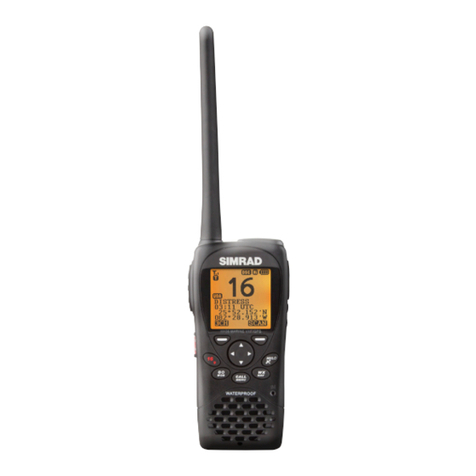
1 INTRODUCTION TO THE HT50 VHF HANDHELD RADIO TELEPHONE
The HT50 transceiver offers high performance, low power consumption, robust
construction and dependable reliability in a small and easy to handle package. The
shockproof casing with push button keys, for ease of operation, is fully waterproofed to a
depth of 1 metre and will withstand the shock of being dropped onto a hard surface from a
height of 1 metre.
The HT50 embraces the following features:
•54 International Channels – plus special national channels
•Dual Watch – on Channel 16 and current working channel
•Tri-Watch – including user selected working channel
•Memory Scan – scans commonly used channels
•All Channel Scan – automatically searches for all incoming signals
•Full Keypad Operation – of all functions including volume and squelch
•Powersave – automatically switches to standby when no signal is
being received
•Rechargeable – 700mAh Nicad Battery with 1200 mAh NimH option
•Battery Charger – for on board charging
The main components of the HT50 are:
1.1 Electronics PCBs
a. Radio Frequency PCB
b. Control PCB
1.2 Mechanical Components
Not yet available

DRAFT
DRAFT 3
2 OPERATING THE HT50 VHF HANDHELD RT
2.1 This Service Manual only contains operating instructions for those features of
the HT50 that are not normally available to the end user. For details of normal
operation please refer to the HT50 Operation Manual, E0XXXX.
2.2 Power ON Combination Functions. There are several functions available
which can only be accessed by pressing and holding down certain key
combinations and switching the radio on. These functions and their method of
activation are described below.
Second Mode. Second Mode (alternative country) – hold down Volume key
and press On.
First Key Beep. When a key is first pressed a beep can be generated. This
function can be toggled on and off by holding down the Squelch key and
pressing the On button. NB. This function can be disabled by
reprogramming the NVM, Section 7 refers.
Programme Mode. The radio is placed in Programme Mode for
programming and reconfiguration utilising a programming kit and a PC. Hold
down SCAN, UP and DW keys and press On. NB. This mode can only be
exited by switching the radio off and whilst in programming mode the radio
will not transmit or receive.
LCD Test Mode. Tests all legends – hold down Volume, Squelch, 16 and
Lights keys and switch On. As each key is operated the appropriate legend
appears. The radio will not transmit or receive in this mode and must be
switched off to exit the mode.
ATIS / DSC Test Mode (only available on special radios). Tone test
mode is activated by holding down the Volume and Scan keys and switching
on. Whilst in this mode the radio receives and transmits on channel 16.
Tests are initiated by pressing keys as follows:
SCAN Radio transmits a continuous ‘0’ tone (2100Hz) Display shows ‘00’
D/W Radio transmits a continuous ‘1’ tone (1300Hz) Display shows ‘11’
LITES Radio transmits alternating ‘010101’ tones Display shows ‘10’
16 Radio receives on channel 16 Display shows ‘16’
Battery Cycle Test Mode (only available on special radios).
The radio can be placed in this mode by holding down the UP & DOWN
keys. While in this mode the radio operates on channel 16 and performs as
follows
•6 seconds receive at full volume unmuted

DRAFT
DRAFT 4
•48 seconds receive with audio muted
•6 seconds transmit at high power
Exit from this mode can only be achieved by turning the radio off.
Tx / Rx Cycle Test Mode (only available on special radios)
The radio can be placed in this mode by holding down the SQUELCH & D/W
keys. While in this mode the radio operates on channel 16 and performs as
follows
•5 minutes receive at full volume unmuted
•5 minutes transmit at high power
Exit from this mode can only be achieved by turning the radio off.

DRAFT
DRAFT 5
3 ASSEMBLY INSTRUCTIONS
Not yet available

DRAFT
DRAFT 6
4 MECHANICAL ASSEMBLY DRAWINGS
4.1 Not yet available

DRAFT
DRAFT 7
5 CIRCUIT DESCRIPTIONS
Introduction
The HT50 consists of 2 PCB assemblies. The RF PCB assembly, Navico Part No.
E03466, contains all the transmitter and receiver circuitry including the synthesiser and
Voltage Controlled Oscillator (VCO). The control PCB assembly, Navico Part No. E03463,
houses the microprocessor, user controls, audio and supply regulation circuitry and the
LCD drivers. The RF and Control PCBs are interconnected via a 20 way multi-connector.
5.1 Radio Frequency PCB. Refer to Drawing No. E03464.
VCO and Frequency Synthesis. A crystal controlled oscillator operating at 21.85
MHz comprising transistor TR10, Crystal Xtal 3 and associated components
provides the reference frequency for the synthesiser and acts as the second Local
Oscillator in the receiver. The synthesiser IC3 is loaded with data from the Control
PCB to select the frequency divide ratios appropriate to the channel selected. The
Voltage Controlled Oscillator (VCO) is tuned by applying the output of the
synthesiser to varactor diode CV2 via the filter C69, R43 and C71. The VCO
operates at the fundamental frequency in transmit mode and at 21.4MHz below the
receive frequency in receive mode. Modulation is achieved by applying the
modulating signal, provided from the Control Board, IC7, to Varactor Diode CV1
and hence to the VCO. The VCO output is fed to buffer amplifiers TR4 and TR5 via
R24 and C47and the output of the buffer is tuned by L11 and L12 with appropriate
capacitors selected, for receive or transmit, by Pin Diodes PD5 and PD6.
Transmitter. The output from the VCO buffer is fed via Pin Diode PD4 and C35 to
the PA Driver stage TR3 which provides about 15 mW drive to the RF Power
Module IC1. Synthesiser IC3 (pin 16) generates an “In Lock” signal, to indicate
that the VCO is in lock, which is applied to transistor TR9. When the VCO is out of
lock, Transistor TR9 inhibits Transistor TR8 and isolates the supply to the PA stage.
Power control is achieved by monitoring the RF output and comparing the rectified
sample with a predetermined level in IC2. Power levels are adjustable through
variable resistor VR1, for low power, and VR2 for high power. The rectified signal
sample is also fed to the Control Board via Transistor TR11 to provide confirmation
that power is being radiated.
The output from the power module is fed via pin diode PD1 to the input/output filter
L1, L2, L3 and associated capacitors. This limits the necessary frequency response
to avoid unwanted harmonic emissions. Pin diode PD2 is enabled when
transmitting to inhibit the signal to the receiver and avoid damage to TR1.
Receiver. The received RF signal from the antenna is applied to a low pass filter
L1, L2, L3, L4 and associated components and to bandpass filter L5 and L6 with
associated capacitors. The signal is amplified by Transistor TR1 and further filtered
by L7 and L8 and associated capacitors.
DRAFT
DRAFT 8
The signal is then applied to mixer TR2 where it is mixed with the VCO output, 21.4
MHz below the signal frequency. The output of the mixer, first Intermediate
Frequency (IF) at 21.4MHz, is matched into the crystal filter network Xtal 1 and Xtal
2 by CH3, C26 and R8. The crystal filter provides isolation from adjacent channel
interference. The crystal filter output is matched to the second IF stage IC4 by CH4
and associated capacitors.
IC4 houses a second mixer amplifier and demodulator. The second mixer mixes
the output of the crystal filter with the output of a crystal controlled oscillator,
operating at 21.85MHz, TR10. The output of the second mixer produces the
second IF, 450KHz, which is filtered by a ceramic filter CF1 to provide further
isolation from adjacent channel interference. The signal is then demodulated in
IC4 and the audio is fed to the control PCB via R61 and C93. The combination of
values of R61, C92 and C96 provide signal de-emphasis.
The audio from pin 9 is also amplified by a high gain amplifier within IC4 to detector
SD2 to provide a voltage proportional to the received signal strength to provide a
noise squelch signal. The squelch signal is fed to an A-D converter on the
microcontroller for comparison with the selected squelch level.

DRAFT
DRAFT 9

DRAFT
DRAFT 10
5.2 Control PCB. All the functions of the radio are controlled from this
assembly by the microprocessor IC10. Refer to Drawing No. E03461.
Power Supply. When the ON / OFF key S1 is pressed TR2 is momentarily
turned on which provides power to the voltage regulators. This in turn powers
up the microcontroller circuit which grounds the base of TR1 and holds TR2
ON.
Voltage regulation is provided by two separate 5 volt regulators, REG1 and
REG2 which provide 5 volt supplies to digital and RF circuitry. TR3 and TR4
respectively route the 5 volts to receive and transmit for the RF and other
analogue circuitry.
To turn the radio off switch S1 is again pressed and held for about 2 seconds.
The continued key depression is sensed by the microcontroller and the base of
TR1 goes high causing loss of supply voltage on release of the key.
Microprocessor. The microprocessor has it own clock controlled by XTAL1
running at 4.096MHz. Reset generator IC8 ensures that the microprocessor
starts up correctly, and resets under low voltage conditions. The
microprocessor has an integral LCD interface driving the front panel display,
LCD1. Voltage drive levels for the LCD driver are produced by the resistor
network R65 – R68. External controls consist of 12 push buttons, S1 to S12
and backlighting is provided by 3 LEDs driven by TR11. The level of
illumination is controlled by the duty cycle applied to the base of TR11.
Configuration data and channel information is stored in the non volatile memory
IC5 which interfaces to IC10 via a 4 wire serial interface.
ATIS Generation and Processing. The ATIS signal is generated by the
microprocessor, IC10, which produces a 2 bit (3 level) approximation of a sine
wave at the correct frequency and baud rate. The two outputs are summed by
R21 – R23 before filtering by IC3b which forms a second order low pass filter.
The output is then attenuated by R100 and R25 before summing into the
microphone audio. Note that the microphone is muted by TR10 during
transmission of the ATIS signal. The MMSI is held in the non volatile memory
IC5 together with a control flag to enable ATIS generation.
The microprocessor also includes software code to enable recognition of ATIS
tones to mute the receiver during reception. The received audio is filtered by
IC9c and IC9d followed by a zero crossing detector formed by IC9a, IC9b, D4
and TR12. This signal is fed to the microprocessor which measures the period
of each half cycle of the incoming signal. By counting the number of periods
which might be an ATIS signal the micro can decide that ATIS is being
received. When this decision is made, after about 10ms, the microprocessor
sets an output to mute the audio for 300ms.
Receive Audio. Audio from the demodulator (on RF PCB) is supplied, via VR1
to preset the maximum audio level, to amplifier IC1a and filter IC1b to provide
rejection of frequencies below 300 Hz. The audio is then fed to the audio power
amplifier stage IC2. The supply to IC2 is controlled by the microprocessor

DRAFT
DRAFT 11
throughTR6 which is turned on only when the radio is in the receive mode and
not squelched.
Volume control is provided by a d.c. level, generated by IC6 and IC11, supplied
to the volume control pin on IC2. IC6 is a shift register which is connected to
the microcontroller and the appropriate volume level is set from information
generated by the raise and lower keys on the front panel when Volume is
selected. This provides a 32 level control of audio.
When any key is pressed a beep is created by the microcontroller generating a
tone, IC10 pin 12, which is filtered by R94, C106, C105 and R93 and fed to the
audio amplifier IC2. TR13 provides momentary muting of the received audio to
increase the clarity of key beeps. If a key beep is required when the radio is
squelched TR16 is turned on to mute the audio whilst the audio amplifier is
turned on via TR6. This is to prevent any clicking from the loudspeaker. As
soon as the key beep has finished, power to the audio amplifier is turned off.
Transmit Audio. DC bias to the microphone is provided by R63 and R64.
When the microphone is not required muting is enabled by the microcontroller
turning on transistor TR10. IC7 and associated components provide
amplification and audio frequency filtering. The circuit also acts as a limiter
using feedback provided by TR8 and TR9. The output from the final amplifier
stage, IC7a is fed via a resistive divider R41, VR3 and R42 to the modulator
diode of the VCO located on the RF PCB.
Communications. To enable programming of the radio a simple serial bi-
directional data link is provided via connection to the antenna socket; isolated
by a network on the RF PCB. This signal is buffered by IC4a and IC4b, for
receive and transmit respectively, and connected to the RxD/TxD lines of the
UART on the microcontroller. When communications are not required the
circuitry is isolated by TR7.

DRAFT
DRAFT 12
LCD
Rotary
Encoder
F
1/25
D/W
Scan
16
Reset
4.096MHz
Reset
4.096MHz
Reverse Power
Carrier Power
Earpiece Audio
Analogue 0V
AF Out
AF In
Squelch Level
PTT / Data Out
Clock, Data &
Enables
Mod out
Mic in
IC6
Main CPU
IC1
IC103a,b IC103c, d D1,
TR11
TR3TR11
VR1
Squelch VR2
IC2a
IC2b
IC5
TR4, TR5
E02958 Circuit Block Diagram

DRAFT
DRAFT 13

DRAFT
DRAFT 14
17.9MHz
VCO &
Buffer Synth
IF Chip
TR301
TR300
XTAL302
XTAL 300,
301
TR302, 302,
VC301
XTAL303
IC300
IC302
IC301
TR305
XTAL304
Osc
DSC AF Out
Clock
Data
Enable 2
E03209 Block Diagram
RF from main
Rx-Tx Board

DRAFT
DRAFT 15
6 CIRCUIT DIAGRAMS
6.1 Circuit Schematics
Radio Frequency PCB E03464
Control PCB E03461

DRAFT
DRAFT 16
Component Lists and Layouts
Radio Frequency PCB Assembly Detail E03466
Control PCB Assembly Detail E03463
Not yet complete

DRAFT
DRAFT 17
7 PROGRAMMING AND CONFIGURATION
Introduction
All Transmitting / Receiving characteristics of the H2 Series radio telephones
are stored in Non Volatile Memory (NVM). The NVM of any H2 Series radio can
be programmed with new characteristics using the programming kit, Part
Number XXXXX.
7.1 Configuration Settings. The following features are available:
COUNTRY Selects primary mode. NVMs with INT
(International) selected for the FIRST
COUNTRY flag will receive on the INT
Rx frequencies. The radio can be
switched to USA with weather
channels if the VOL key is depressed
on power up unless the SELECTED
MODE ONLY flag is set.
(SECOND MODE – YES).
SECOND MODE Enables or disables switch to USA with
weather channels.
SCANNING Enables and disables SCAN and
MEMORY SCAN functions.
CHANNEL 10 SCAN Enables or disables Channel 10 from
SCAN facility, (Scanning Channel 10 is
not permitted in some countries).
DUAL WATCH Enables or disables DUAL WATCH
TRI WATCH Enables or disables TRI WATCH
PRIORITY CHANNEL Selects alternate channel to be
monitored when DUAL WATCH
selected.
FIRST KEY BEEP Enables or disables KEY BEEP
STARTUP CHANNEL (SC) Selects channel to be displayed on
power up, usually Channel 16
WATCH CHANNEL (WC) Selects third channel to be monitored
when TRI WATCH selected.
USA / CANADA Enables or disables USA weather
WEATHER CHANNELS channels.

DRAFT
DRAFT 18
ATIS IDENTIFIER Stores Automatic Transmission
Identification System (ATIS)
DSC IDENTIFIER Maritime Mobile Service Identity
(MMSI) number.
7.2 Programming.
INITIAL SET UP
The XXXXX programming kit operates in conjunction with an IBM compatible
PC. The programme should be copied to the 'C’ drive on the PC hard disc into
a directory entitled H2setup.exe
C:\H2setup.exe
If using a monochrome monitor type MODE BW80. Connection between the
radio and PC is by means of the programming lead supplied with the kit from
the Antenna Socket on the radio to a 9 pin serial port on the PC.
Enter the programming set up software by typing “H2setup”. Programming is
entirely menu driven and self explanatory. (NB. Programme may not run under
WINDOWS 95 / 97 / 98 but operates satisfactorily under 3.1 or 3.11).
H2 RADIO SETUP PROGRAM
---------------------------------------------------------
Version 1.0
Copyright (C) Simrad-Navico Ltd 1998
This program allows the dealer to configure the H2 series
Radios to any mode including the programming of private channels.
WARNING
--------------
Incorrect use of this program could enable the radios to be used
in contravention of local regulations.
Which COM port is to be used? (1 or 2)
Type 1, 2 or [ESC] to exit program
In order to adjust characteristics, radio must be switched to
“Programming Mode”
by:
simultaneously holding down SHIFT, UP and DW keys
whilst pressing ON key

DRAFT
DRAFT 19
H2 RADIO SETUP PROGRAM
---------------------------------------------------------
Using COM1 port on computer NVM Data: NOT LOADED
Select option:-
1 - Load NVM data from Radio (Copy data from radio to PC)
2 - Load NVM data from File (Load data from programme file)
3 - View/Modify NVM data (View/change displayed data)
4 - Save NVM data to Radio (Save displayed data to radio)
5 - Save NVM data to File (Save data to new PC file)
6 - CLONE from existing Radio (Copy existing data from radio to radio)
7 – Exit Program (Exit programme)
Use ↑↓ [Enter] or type option number, type [ESC] to exit program
**Text in brackets is for information only and does not appear on screen**
Load NVM data from Radio
Connect Radio, press any key when ready
NVM data
00: 10: 20: 30:
01: 11: 21: 31:
02: 12: 22: 32:
03: 13: 23: 33:
04: 14: 24: 34:
05: 15: 25: 35:
06: 16: 26: 36:
07: 17: 27: 37:
08: 18: 28: 38:
09: 19: 29: 39:
0A: 1A: 2A: 3A:
0B: 1B: 2B: 3B:
0C: 1C: 2C: 3C:
0D: 1D: 2D: 3D:
0E: 1E: 2E: 3E:
0F: 1F: 2F: 3F:
Any key to continue, [ESC] to exit

DRAFT
DRAFT 20
Load NVM data from Radio
Connect Radio, press any key when ready
Failed - check connections, is radio turned on?
NVM data
00: 10: 20: 30:
01: 11: 21: 31:
02: 12: 22: 32:
03: 13: 23: 33:
04: 14: 24: 34:
05: 15: 25: 35:
06: 16: 26: 36:
07: 17: 27: 37:
08: 18: 28: 38:
09: 19: 29: 39:
0A: 1A: 2A: 3A:
0B: 1B: 2B: 3B:
0C: 1C: 2C: 3C:
0D: 1D: 2D: 3D:
0E: 1E: 2E: 3E:
0F: 1F: 2F: 3F:
Any key to continue, [ESC] to exit
Load NVM data from Radio
Connect Radio, press any key when ready
NVM data loaded successfully
NVM data
00: 0010 10: 0003 20: 0000 30: 0000
01: 0000 11: 3011 21: 0000 31: 0000
02: 2020 12: 1111 22: 0000 32: 0000
03: 8008 13: 1111 23: 0000 33: 0000
04: 1010 14: 1333 24: 0000 34: 0000
05: 3111 15: 3333 25: 0000 35: 0000
06: 1101 16: 3333 26: 0000 36: 0000
07: 0000 17: 3300 27: 0000 37: 0000
08: 0004 18: 3333 28: 0000 38: 0000
09: 0411 19: 3333 29: 0000 39: 0000
0A: 1111 1A: 3333 2A: 0000 3A: 0000
0B: 1111 1B: 33FF 2B: 0000 3B: 0000
0C: 1333 1C: 3098 2C: A1A2 3C: 0000
0D: 1111 1D: 309A 2D: FFFF 3D: 0010
0E: 1110 1E: 0000 2E: 0000 3E: 1010
0F: 0030 1F: 0000 2F: 0000 3F: 016A
Any key to continue, [ESC] to exit
Other manuals for HT50
2
Table of contents
Other Simrad Radio manuals

Simrad
Simrad RS90S User manual

Simrad
Simrad Shipmate RS8400 Reference manual

Simrad
Simrad RS86 User manual

Simrad
Simrad RS20 User manual

Simrad
Simrad HT50 User manual

Simrad
Simrad RS81 User manual

Simrad
Simrad Axis30 User manual

Simrad
Simrad RS10U User manual

Simrad
Simrad RS90S User manual

Simrad
Simrad SHIPMATE RS8100 User manual

Simrad
Simrad RD68 User manual

Simrad
Simrad HT50 User manual

Simrad
Simrad RD68 User manual

Simrad
Simrad RS20S User manual

Simrad
Simrad WR20 RemoteCommander User manual

Simrad
Simrad FishNet 144 User manual

Simrad
Simrad RS40 User manual

Simrad
Simrad RT62 User manual

Simrad
Simrad RS25-E User manual

Simrad
Simrad RD68 User manual