– 13 – – 14 –
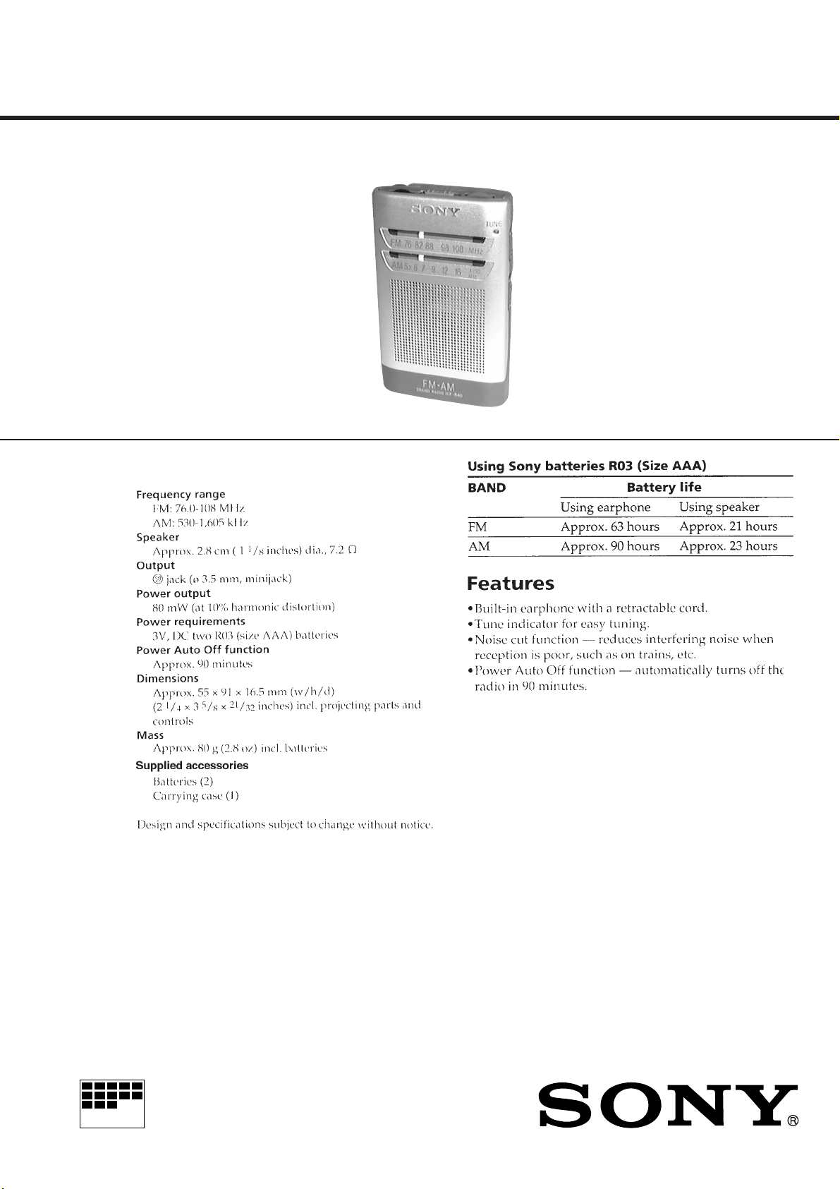
SECTION 6
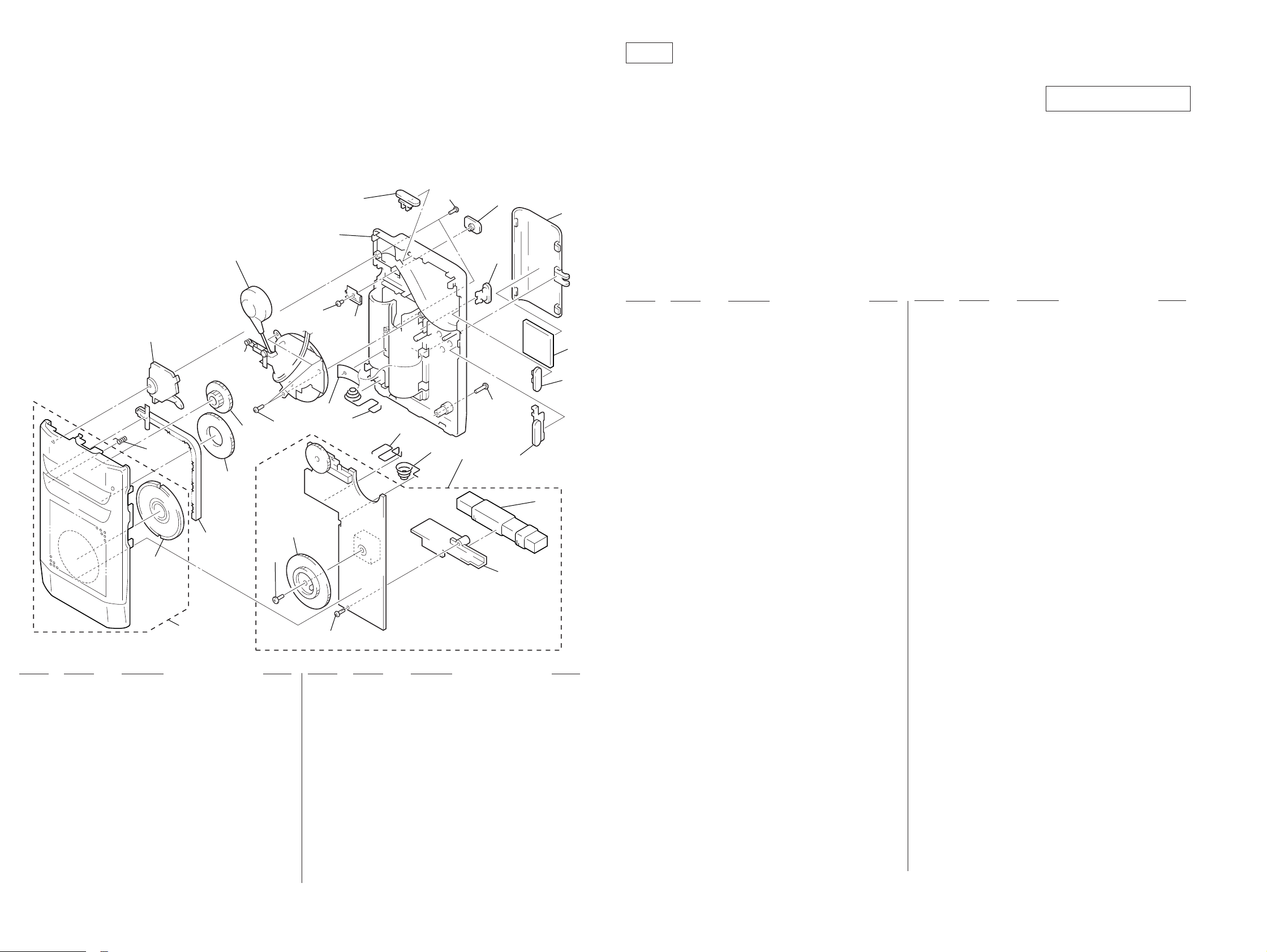
EXPLODED VIEW
• Items marked “*” are not stocked since they
are seldom required for routine service. Some
delay should be anticipated when ordering
these items.
• The mechanical parts with no reference num-
ber in the exploded views are not supplied.
• Accessories and packing materials are given
in the last of the electrical parts list.
NOTE:
• -XX and -X mean standardized parts, so they
may have some difference from the original
one.
• Color Indication of Appearance Parts
Example:
KNOB, BALANCE (WHITE) . . . (RED)
↑↑
Parts Color Cabinet's Color
Ref. No. Part No. Description Remark Ref. No. Part No. Description Remark
SECTION 7
ELECTRICAL PARTS LIST
Ref. No. Part No. Description Remark
NOTE:
• Due to standardization, replacements in the
parts list may be different from the parts speci-
fied in the diagrams or the components used
on the set.
• -XX and -X mean standardized parts, so they
may have some difference from the original
one.
• RESISTORS
All resistors are in ohms.
METAL: Metal-film resistor.
METAL OXIDE: Metal oxide-film resistor.
F: nonflammable
• Items marked “*” are not stocked since they
are seldom required for routine service.
Some delay should be anticipated when order-
ing these items.
• SEMICONDUCTORS
In each case, u: µ, for example:
uA. . : µA. . uPA. . : µPA. .
uPB. . : µPB. . uPC. . : µPC. .
uPD. . : µPD. .
• CAPACITORS
uF: µF
• COILS
uH: µH
Ref. No. Part No. Description Remark
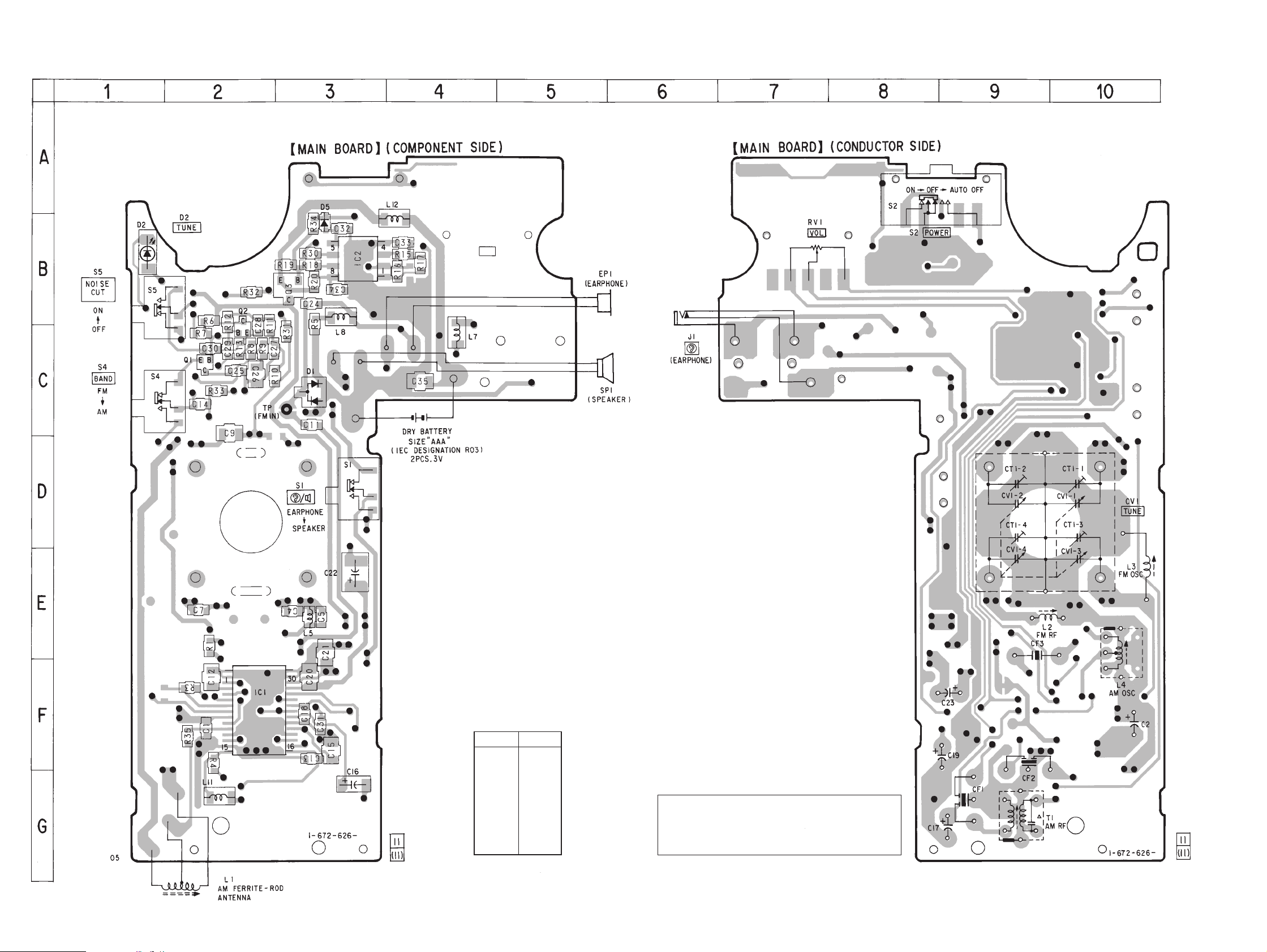
When indicating parts by reference
number, please include the board.
MAIN
1 A-3638-700-A CABINET (FRONT) ASSY
2 3-034-344-01 POINTER
3 3-034-347-01 GEAR (MIDWAY)
4 3-034-348-01 KNOB (TUNE)
5 3-895-823-11 SCREW (B1.4X3), TAPPING
6 A-3638-697-A REEL ASSY
7 3-032-525-01 SCREW
8 3-032-492-01 PLATE (REWIND)
9 3-034-341-21 CABINET (REAR)
10 3-034-349-01 KNOB (POWER)
11 3-015-033-01 SCREW (DIA. 1.4X4), PRECISION
12 3-034-352-01 LID, BATTERY CASE
13 3-034-357-01 COMBINED (KNOB) (including
KNOB (REWIND), KNOB (EARPHONE/
SPEAKER),KNOB (NOISE CUT),
KNOB (2 BAND))
14 3-910-816-01 SCREW (M1.7x10)
15 3-034-212-01 TERMINAL (+/–), BATTERY
16 3-034-210-01 TERMINAL (+), BATTERY
17 3-034-211-01 TERMINAL (–), BATTERY
*18 A-3683-046-A MAIN BOARD, COMPLETE
19 3-034-358-01 COMBINED (BLIND PLATE) (including
BLIND PLATE, HOLDER (BAR ANTNNA))
20 3-880-990-00 SCREW (1.7X3), FLAT, (+) SPECIAL
21 3-034-346-01 GEAR (TUNING CAPACITOR)
22 3-384-797-01 SCREW (1.4X4)
23 3-036-666-01 SPRING (ELECTROSTATIC)
24 9-911-816-01 CLOTH, BATTERY PICK
25 3-831-441-99 CUSHION (A)
L1 1-754-049-11 ANTENNA, FERRITE-ROD (AM)
SP1 1-529-187-11 SPEAKER (2.8cm)
4
A
r
B
r
C
r
D
(including
r
B,
r
C,
r
D
(including
4
A)
L1
SP1
1
2
3
45
6
78
9
10 11 12
13
14
15
24
16
17 18
19
21
22
20
23
25
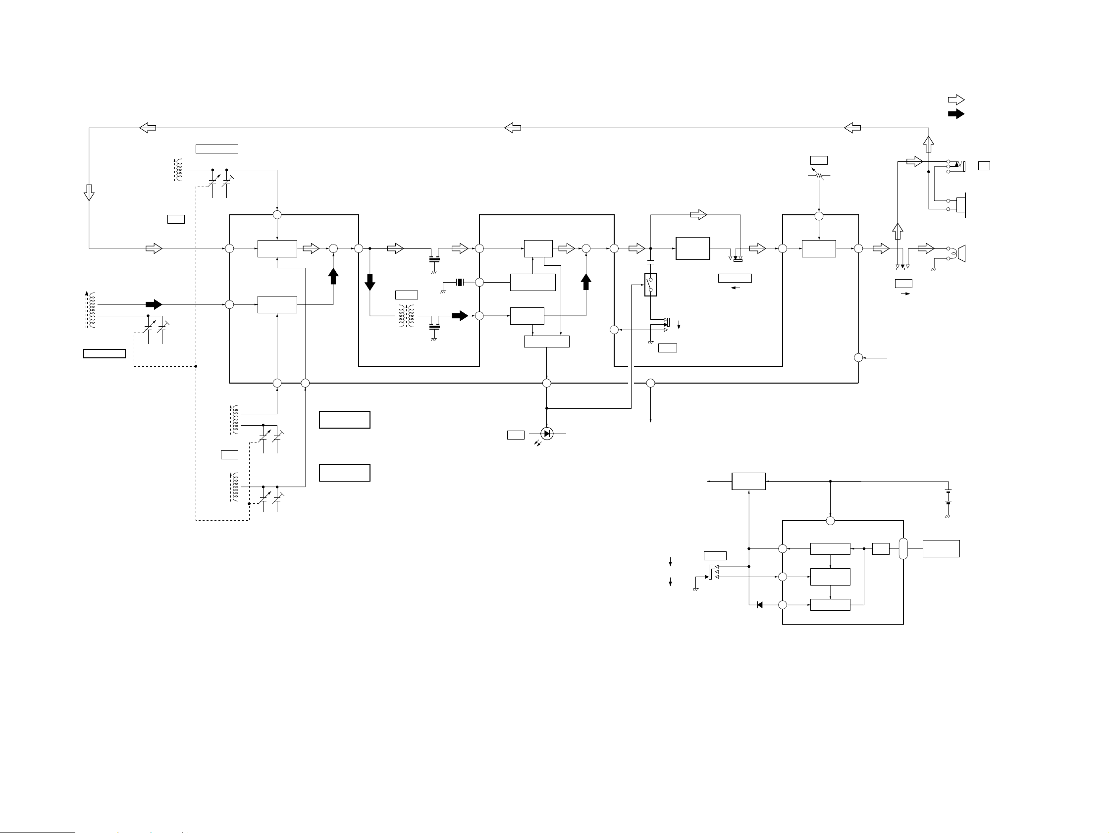
*A-3683-046-A MAIN BOARD, COMPLETE
*********************
3-034-346-01 GEAR (TUNING CAPACITOR)
3-034-358-01 COMBINED (BLIND PLATE) (including BLIND
PLATE, HOLDER (BAR ANTENNA))
3-384-797-01 SCREW (1.4X4)
3-880-990-00 SCREW (1.7X3), FLAT, (+) SPECIAL
<CAPACITOR>
C1 1-162-970-11 CERAMIC CHIP 0.01uF 10% 25V
C2 1-126-157-11 ELECT 10uF 20% 16V
C4 1-162-919-11 CERAMIC CHIP 22PF 5% 50V
C5 1-162-922-11 CERAMIC CHIP 39PF 5% 50V
C7 1-162-917-11 CERAMIC CHIP 15PF 5% 50V
C9 1-164-275-91 CERAMIC CHIP 9PF 5% 50V
C11 1-162-927-11 CERAMIC CHIP 100PF 5% 50V
C12 1-164-346-11 CERAMIC CHIP 1uF 16V
C13 1-162-970-11 CERAMIC CHIP 0.01uF 10% 25V
C14 1-164-156-11 CERAMIC CHIP 0.1uF 25V
C15 1-164-346-11 CERAMIC CHIP 1uF 16V
C16 1-135-151-21 TANTALUM CHIP 4.7uF 20% 4V
C17 1-126-157-11 ELECT 10uF 20% 16V
C18 1-164-227-11 CERAMIC CHIP 0.022uF 10% 25V
C19 1-126-157-11 ELECT 10uF 20% 16V
C20 1-164-346-11 CERAMIC CHIP 1uF 16V
C21 1-164-346-11 CERAMIC CHIP 1uF 16V
C22 1-127-569-11 TANTAL. CHIP 100uF 20% 4V
C23 1-124-434-00 ELECT 220uF 20% 4V
C24 1-162-927-11 CERAMIC CHIP 100PF 5% 50V
C25 1-165-176-11 CERAMIC CHIP 0.047uF 10% 16V
C26 1-164-346-11 CERAMIC CHIP 1uF 16V
C27 1-164-156-11 CERAMIC CHIP 0.1uF 25V
C28 1-164-227-11 CERAMIC CHIP 0.022uF 10% 25V
C29 1-164-677-11 CERAMIC CHIP 0.033uF 10% 16V
C30 1-164-227-11 CERAMIC CHIP 0.022uF 10% 25V
C31 1-162-964-11 CERAMIC CHIP 0.001uF 10% 50V
C32 1-164-156-11 CERAMIC CHIP 0.1uF 25V
C33 1-162-968-11 CERAMIC CHIP 0.0047uF 10% 50V
C34 1-164-156-11 CERAMIC CHIP 0.1uF 25V
C35 1-164-346-11 CERAMIC CHIP 1uF 16V
<CERAMIC FILTER>
CF1 1-567-177-00 FILTER, CERAMIC (455kHz)
CF2 1-579-632-51 FILTER, CERAMIC (10.7MHz)
CF3 1-579-632-51 FILTER, CERAMIC (10.7MHz)
<VARIABLE CAPACITOR>
CT1 1-141-607-11 CAP, VAR
CV1 1-141-607-11 CAP, VAR (TUNE)
<DIODE>
D1 8-719-800-76 DIODE 1SS226
D2 8-719-062-42 LED BR1111R-TR (TUNE)
D5 8-719-046-91 DIODE MA2S111
<IC>
IC1 8-752-036-29 IC CXA1280N
IC2 8-759-583-17 IC BU2305F-E2
<JACK>
J1 1-785-506-11 JACK (@)
<COIL>
L1 1-754-049-11 ANTENNA, FERRITE-ROD (AM)
L2 1-419-109-11 COIL, AIR-CORE
L3 1-419-108-11 COIL, AIR-CORE
L4 1-406-255-11 COIL (OSC)
L5 1-412-971-31 INDUCTOR 0.22uH
L7 1-412-947-11 INDUCTOR 4.7uH
L8 1-412-947-11 INDUCTOR 4.7uH
L11 1-412-947-11 INDUCTOR 4.7uH
L12 1-412-947-11 INDUCTOR 4.7uH
<TRANSISTOR>
Q1 8-729-037-71 TRANSISTOR UN9210J-(TX).SO
Q2 8-729-037-92 TRANSISTOR 2SD2216J-R(TX).SO
Q3 8-729-800-71 TRANSISTOR 2SB815B7-TB
<RESISTOR>
R1 1-216-813-11 METAL CHIP 220 5% 1/16W
R3 1-216-845-11 METAL CHIP 100K 5% 1/16W
R4 1-216-817-11 METAL CHIP 470 5% 1/16W