Sony HCD-CP1 User manual

SERVICE MANUAL
MICRO HiFi COMPONENT SYSTEM
SPECIFICATIONS
HCD-CP1
Dolby noise reduction manufactured under license
from Dolby Laboratories Licensing Corporation.
“DOLBY” and the double-D symbol aare trade-
marks of Dolby Laboratories Licensing Corporation.
US Model
Canadian Model
AEP Model
UK Model
E Model
Australian Model
HCD-CP1istheAmplifier,CDplayer,
Tape Deck and Tuner section in
CMT-CP1.
–Continued on next page –
Model Name Using Similar Mechanism NEW
CD Mechanism Type KSL-2130CCP/K1N
Optical Pick-up Name KSS-213C/K1N
Model Name Using Similar Mechanism HCD-ED1
Tape Transport Mechanism Type CMAL1Z023A
CD
Section
Tape deck
Section
Note
CD block,tape deck block and
tuner pack are supplied with
the assembled block.
Ver 1.1 2001.02
With SUPPLEMENT-1
(9-928-809-81)
9-928-809-12 Sony Corporation
2001B0500-1 Audio Entertainment Group
C2001.2 General Engineering Dept.

– 2 –

– 3 –
1. SERVICING NOTES ............................................... 3
2. GENERAL
Location of Controls ....................................................... 5
Setting the Time .............................................................. 6
3. DISASSEMBLY ......................................................... 7
4. SERVICE MODE...................................................... 11
5. ELECTRICAL CONFIRMATIONS AND
ADJUSTMENTS
DECK Section ................................................................. 12
6. DIAGRAMS
6-1. Block Diagram – TAPE Section – .................................. 15
6-2. Block Diagram – MAIN Section – ................................. 17
6-3. Block Diagram
– DISPLAY/POWER SUPPLY Section – ...................... 19
6-4. Note for Printed Wiring Boards and
Schematic Diagrams ....................................................... 21
6-5. Printed Wiring Board – MAIN Section – ....................... 23
6-6. Schematic Diagram – MAIN Section (1/4) –................. 25
6-7. Schematic Diagram – MAIN Section (2/4) –................. 27
6-8. Schematic Diagram – MAIN Section (3/4) –................. 29
6-9. Schematic Diagram – MAIN Section (4/4) –................. 31
6-10. Printed Wiring Boards
– PANEL/CD LOADING Section – ............................... 33
6-11. Printed Wiring Boards – CONTROL Section – ............. 37
6-12. Schematic Diagram – CONTROL Section –.................. 39
6-13. Printed Wiring Board – POWER Section –.................... 41
6-14. Schematic Diagram – POWER Section – ...................... 42
6-15. IC Pin Function Description ........................................... 43
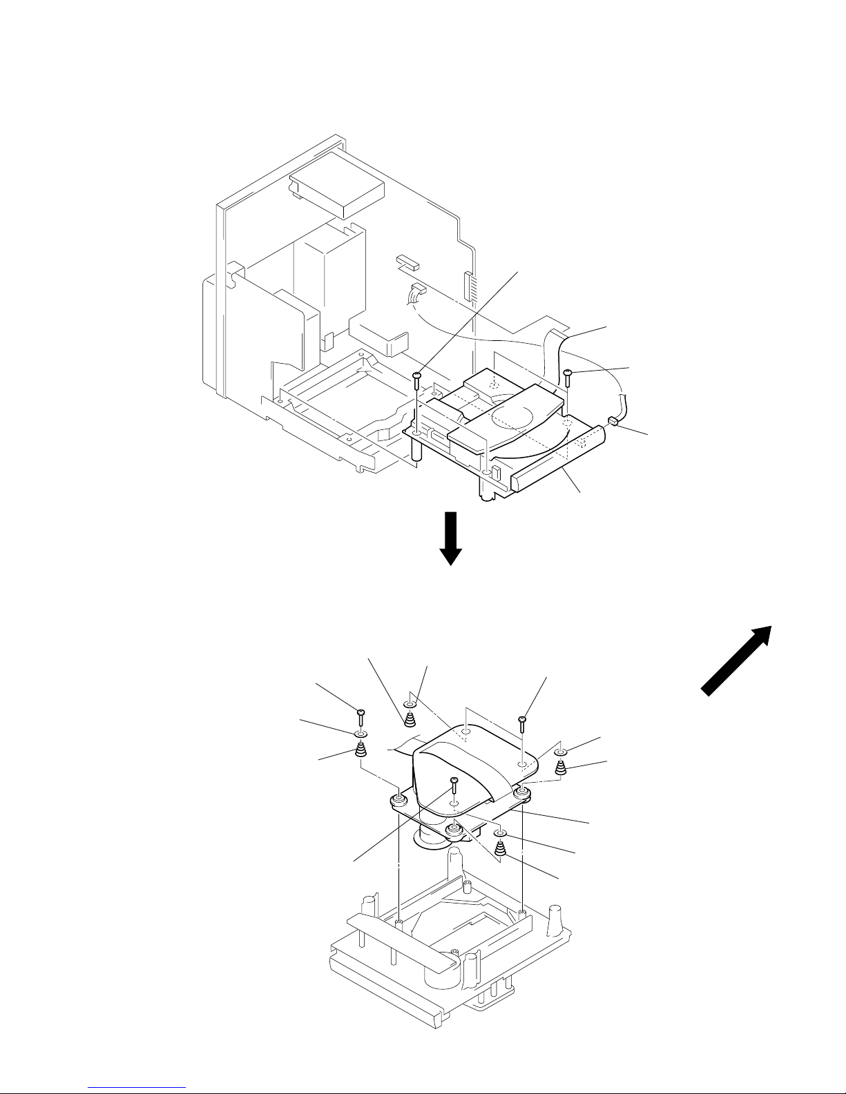
7. EXPLODED VIEWS................................................ 45
8. ELECTRICAL PARTS LIST ............................... 49
TABLE OF CONTENTS SECTION 1
SERVICING NOTES
The laser diode in the optical pick-up block may suffer electro-
static break-down because of the potential difference generated
by the charged electrostatic load, etc. on clothing and the human
body.
During repair, pay attention to electrostatic break-down and also
use the procedure in the printed matter which is included in the
repair parts.
The flexible board is easily damaged and should be handled with
care.
NOTES ON LASER DIODE EMISSION CHECK
The laser beam on this model is concentrated so as to be focused
on the disc reflective surface by the objective lens in the optical
pick-up block. Therefore, when checking the laser diode emis-
sion, observe from more than 30 cm away from the objective lens.
Notes on chip component replacement
• Never reuse a disconnected chip component.
• Notice that the minus side of a tantalum capacitor may be dam-
aged by heat.
Flexible Circuit Board Repairing
• Keep the temperature of the soldering iron around 270 ˚C dur-
ing repairing.
• Do not touch the soldering iron on the same conductor of the
circuit board (within 3 times).
• Be careful not to apply force on the conductor when soldering
or unsoldering.
NOTES ON HANDLING THE OPTICAL PICK-UP
BLOCK OR BASE UNIT
CAUTION
Use of controls or adjustments or performance of procedures
other than those specified herein may result in hazardous ra-
diation exposure.
This appliance is classified as a CLASS 1 LASER product.
The CLASS 1 LASER PRODUCT MARKING is located on
the rear exterior.
Laser component in this product is capable of emitting radiation
exceeding the limit for Class 1.
The following caution label is located inside the unit.
CAUTION : INVISIBLE LASER RADIATION WHEN OPEN AND
INTERLOCKS DEFEATED. AVOID EXPOSURE TO BEAM.
ADVARSEL : USYNLIG LASERSTRÅLING VED ÅBNING NÅR
SIKKERHEDSAFBRYDERE ER UDE AF FUNKTION. UNDGÅ UDSAETTELSE
FOR STRÅLING.
VORSICHT : UNSICHTBARE LASERSTRAHLUNG, WENN
ABDECKUNG GEÖFFNET UND SICHEREITSVERRIEGELUNG
ÜBERBRÜCKT. NICHT DEM STRAHL AUSSETZEN.
VARO
!
:AVATTAESSA JA SUOJALUKITUS OHITETTAESSA OLET ALT-
TIINA NÄKYMÄTTÖMÄLLE LASERSÄTEILYLLE. ÄLÄ KATSO SÄTEESEEN.
VARNING : OSYNLING LASERSTRÅLING NÄR DENNA DEL ÄR ÖPPNAD
OCH SPÄRREN ÄR URKOPPLAD.BETRAKTA EJ STRÅLEN.
ADVERSEL : USYNLIG LASERSTRÅLING NÅR DEKSEL ÅPNES OG
SIKKERHEDSLÅS BRYTES. UNNGÅ EKSPONERING FOR STRÅLEN.
VIGYAZAT
!
:A BURKOLAT NYITÁSAKOR LÁTHATATLAN LÉZERSU-
GÁRVESZÉLY
!
KERÜLJE A BESUGÁRZÁST
!

– 4 –
ATTENTION AU COMPOSANT AYANT RAPPORT
À LA SÉCURITÉ!
LES COMPOSANTS IDENTIFIÉS PAR UNE MARQUE !
SUR LES DIAGRAMMES SCHÉMATIQUES ET LA LISTE
DES PIÈCES SONT CRITIQUES POUR LA SÉCURITÉ
DE FONCTIONNEMENT. NE REMPLACER CES COM-
POSANTS QUE PAR DES PIÈCES SONY DONT LES
NUMÉROS SONT DONNÉS DANS CE MANUEL OU
DANS LES SUPPLÉMENTS PUBLIÉS PAR SONY.
SAFETY-RELATED COMPONENT WARNING!!
COMPONENTS IDENTIFIED BY MARK !OR DOTTED
LINE WITH MARK !ON THE SCHEMATIC DIAGRAMS
AND IN THE PARTS LIST ARE CRITICAL TO SAFE
OPERATION. REPLACE THESE COMPONENTS WITH
SONY PARTS WHOSE PART NUMBERS APPEAR AS
SHOWN IN THIS MANUAL OR IN SUPPLEMENTS PUB-
LISHED BY SONY.
SAFETY CHECK-OUT
After correcting the original service problem, perform the follow-
ing safety check before releasing the set to the customer:
Check the antenna terminals, metal trim, “metallized” knobs,
screws, and all other exposed metal parts for AC leakage.
Check leakage as described below.
LEAKAGE TEST
TheAC leakage from any exposed metal part to earth ground and
from all exposed metal parts to any exposed metal part having a
return to chassis, must not exceed 0.5 mA (500 microampers.).
Leakage current can be measured by any one of three methods.
1. A commercial leakage tester, such as the Simpson 229 or RCA
WT-540A. Follow the manufacturers’instructions to use these
instruments.
2. A battery-operatedAC milliammeter. The Data Precision 245
digital multimeter is suitable for this job.
3. Measuring the voltage drop across a resistor by means of a
VOM or battery-operated AC voltmeter. The “limit” indica-
tion is 0.75 V, so analog meters must have an accurate low-
voltage scale. The Simpson 250 and Sanwa SH-63Trd are ex-
amples of a passive VOM that is suitable. Nearly all battery
operated digital multimeters that have a 2V AC range are suit-
able. (See Fig. A)
Fig. A. Using an AC voltmeter to check AC leakage.
1.5 k
Ω
0.15
µ
FAC
voltmeter
(0.75 V)
To Exposed Metal
Parts on Set
Earth Ground
MODEL IDENTIFICATION
– Back Panel –
Power Voltage Indication
VOLTAGE SELECTOR
Switch
Model Power Voltage
Incdication
US, Canadian models AC: 120 V 60 Hz 55 W
AEP, UK models AC: 230 V ⁄50 Hz 55 W
Malaysia, Singapore, AC: 110 – 120/
Hong Kong and 220 – 240 V ⁄50/60 Hz 55 W
Thai models

– 5 –
SECTION 2
GENERAL
LOCATION OF CONTROLS
• Front View 1TAPE deck
2Liquid crystal display
3TAPE Pbutton
4TAPE 0button
5TAPE œbutton
6TAPE 6button
7TAPE pbutton
8TAPE )button
9TAPE REC rbutton
0CD SYNC button and indicator
!¡ BAND button
!™ TUNING + button
!£ TUNING – button
!¢ TUNING MODE button
!∞ CD EJECT 6button
!§ CD pbutton
!¶ CD +)button
!• CD REPEAT button
!ª DSG button and indicator
@º STANDBY 1/ubutton and indicator
@¡ MD/VIDEO button and indicator
@™ TAPE button and indicator
@£ CD button and indicator
@¢ TUNER button and indicator
@∞ Remote sensor
@§ PHONES jack
@¶ CD disc tray
@• VOLUME knob
@ª CD ^button
#º CD =0button
#¡ CD PLAY MODE button
1AM ANTENNA terminals
2FM ANTENNA jack or terminals
3VOLTAGE SELECTOR switch
(Malaysia, singapore and Hong Kong)
4LINE OUT jacks
5MD IN jacks
6VIDEO IN jacks
7CD DIGITAL OUT OPTICAL connector
8SPEAKER terminals
1 2 3 4 5 6
8
7
9
!º
!¡
!™
!¶
!§
!∞
!£
!¢
!ª
@º
@¡
@™
@£
@¢
@∞
@§ @¶ @• @ª #¡
!•
#º
21
3
4
5
6
7
8
• Rear View

– 6 –
This section is extracted from
instruction manual.

– 7 –
COVER (UPPER)
TAPE MECHANISM DECK
Note: Follow the disassembly procedure in the numerical order given.
SECTION 3
DISASSEMBLY
1
two screws
(case3 TP2)
3
cover (upper)
2
four screws
(BTP3
×
8)
1
two screws
(case3 TP2
)
5
two screws
2
connector
4
tape
mechanism deck
1
flat wire (12 core)
3
two screws
(BTP3
×
8)
3
two screws
(BTP3
×
8)
6
motor
7
main belt
8
F/R belt
9
claw
0
pinch roller

– 8 –
FRONT PANEL SECTION
• FRONT PANEL SECTION INSTALLATION
Note: Follow the assembly procedure in the numerical order given.
1connector
(CN303)
1connector
1connector
(CN809)
2two flat wires
(CN802, 804)
2flat wire
(12 core)
5two claws
3screw
(KTP3 ×6)
7front panel section
6connector (CN603
)
4two screws
(BTP3 ×8)
3screw
(KTP3 ×6)
6connector
5flat wire (12 core)
5two flat wires
(CN802, 804)
6two connectors
(CN303, 809)
2connector
(CNP806)
Note: As CNP806 pin is bent easily,
treat is carefully.
3screw
(KTP3 ×6)
4two screws
(BTP3 ×8)
3screw
(KTP3 ×6)
1two claws

– 9 –
CD MECHANISM DECK
BU ASS’Y
3
two screws
(BTP3
×
8)
3
two screws
(BTP3
×
8)
2
flat wire (19 core)
(CN805)
1
connector
4
CD mechanism deck
1
screw
(P2.6
×
10)
3
coil spring
(front)
3
coil spring
(rear)
3
coil spring
(rear)
2
washer
2
washer
2
washer
3
coil spring
(front)
2
washer
1
screw
(P2.6
×
10)
1
two screws
(P2.6
×
10)
4
BU ass’y
Note: As
3
coil springs are missed easily, treat them carefully.

– 10 –
4
Pull the tray.
8
Remove the tray.
7
lock lever
1
two screws
(PTPWH2.6
×
7)
2
chucking yoke (K)
6
damper (S)
5
claw
7
lock lever
3
Rotate the control cam
in the direction of arrow
A
.
A
TRAY
• SUB CHASSIS INSTALLATION
Note: Follow the assembly procedure in the numerical order given.
2
Install the drive gear with gear
position as shown in figure.
gear
front side
1
Install the control cam
with gear position as shown
in figure.
gear
front side
3
screw
(PTPWH2.6
×
16)
5
two screws
(PTPWH2.6
×
7)
4
sub chassis

– 11 –
SECTION 4
SERVICE MODE
[Liquid Crystal Display All Lit Check Mode]
Procedure:
1. Set to standby state.
2. Press three buttons of p(TAPE), p(CD), and [MD/VIDEO]
simultaneously.
3. Liquid crystal display are all turned on.
4. To exit from this mode, press the 1/ubutton to turn the power
OFF.
[Tape Deck Aging Mode]
This mode can be used for operation check of tape deck section.
Procedure:
1. Set a tape in the tape deck.
2. Set to standby state.
3. Press three buttons of p(TAPE), p(CD), and [TAPE] si-
multaneously.
4. The aging is executed in bellow sequence.
5. To exit from the aging mode, press the 1/ubutton to turn the
power OFF.
Aging mode sequence:
[CD Aging Mode]
This mode can be used for operation check of CD section.
Procedure:
1. Load a CD disc.
2. Set to standby state.
3. Press three buttons of p(TAPE), p(CD), and [TUNER]
simultaneously.
4. The aging is executed in bellow sequence.
5. To exit from the aging mode, press the 1/ubutton to turn the
power OFF.
Aging mode sequence:
Start
REC pause for 3 seconds
FWD REC
Fast forward
REV Play
REC pause for 3 seconds
REV REC
Rewind
FWD Play Shut off
Shut off
Shut off
Shut off
1 minute
3 minutes
1 minute
3 minutes
Start
Open the disc tray
Close the disc tray
Play the last track

– 12 –
SECTION 5
ELECTRICAL CONFIRMATIONS AND ADJUSTMENTS
0 dB=0.775 V
DECK SECTION
Tape Signal Used for
P-4-A100 10 kHz, –10 dB Azimuth Adjustment
WS-48B 3 kHz, 0 dB Tape Speed Adjustment
P-4-L300 315 Hz, 0 dB Level Adjustment
Note: Confirm each contents of this section first of all. If the results are
not satisfied, do the adjustment.
1. Demagnetize the record/playback head with a head demagne-
tizer.
2. Do not use a magnetized screwdriver for the adjustments.
3. After the adjustments, apply suitable locking compound to the
parts adjust.
4. The adjustments should be performed with the rated power
supply voltage unless otherwise noted.
5. The adjustments should be performed in the order given in
this service manual. (As a general rule, playback circuit ad-
justment should be completed before performing recording
circuit adjustment.)
6. The adjustments should be performed for both L-CH and R-
CH.
7. Switches and controls should be set as follows unless other-
wise specified.
• Test Tape
Record/Playback Head Azimuth Adjustment
Procedure:
1. Mode: Playback
set
MAIN board
LINE OUT jack (PJ301)
L-CH, R-CH
+
–
level mete
r
test tape
P-4-A100
(10 kHz, –10 dB)
Screw
position
L-CH
peak
within
1dB
Output
level
L-CH
peak R-CH
peak
within
1dB
Screw
position
R-CH
peak
2. Turn the adjustment screw and check output peaks. If the peaks
do not match for L-CH and R-CH, turn the adjustment screw
so that outputs match within 1dB of peak.
3. Mode: Playback
4. Repeat step 1 to 3 in playback (REV) mode.
5. After the adjustments, apply suitable locking compound to the
pats adjusted.
Adjustment Location:
MAIN
board
CN301
set
test tape
P-4-A100
(10 kHz, –10 dB)
R-CH
oscilloscope
L-CH
R-CH
VH
waveform of oscilloscope
in phase 45
°
90
°
135
°
180
°
good wrong
MAIN board
LINE OUT jack (PJ301)
L-CH
forward
reverse

– 13 –
Playback level Confirmation and Adjustment
Procedure:
Mode: Playback
Confirm playback level is within specification values as follows.
If these levels are out of specification values, adjust the RV151
(L-CH) and RV251 (R-CH) on the MAIN board so that the level
meter reading become within specification values.
Specification values:
PJ301 PB level: 301.5 to 338.3 mV (–8.2 to –7.2 dB) level differ-
ence between the channels: within ±0.5 dB
Adjustment Location: MAIN board
REC Bias Confirmation and Adjustment
Procedure:
1. Mode: Record
2. Mode: Playback
3. Confirm playback the signal recorded in step 1 become speci-
fication values as follows.
If these values are out of specification values, adjust the RV153
(L-CH) and RV253 (R-CH) on the MAIN board to repeat steps
1and 2.
Specification values: Playback output of 315 Hz to playback out-
put of 10 kHz: ± 0.5 dB
Adjustment Location: MAIN board
+
–
set
test tape
WS-48B
(3 kHz, 0 dB)
MAIN board
LINE OUT jack (PJ301)
L-CH, R-CH
frequency counter
REC Level Confirmation and Adjustment
Procedure:
1. Mode: Record
2. Mode: Playback
3. Confirm playback the signal recorded in step 1 become speci-
fication values as follows.
If these values are out of specification values, adjust the RV252
(R-CH) and RV152 (L-CH) on the MAIN board to repeat steps
1 and 2.
Specification values:
PJ301 PB level: 47.2 to 53.0 mV (– 24.3 to – 23.3 dB)
Adjustment Location: MAIN board
– MAIN BOARD (Conductor Side) –
attenuator
set
MAIN board
MD IN jack (PJ301)
L-CH, R-CH
1) 315 Hz
2) 10 kHz 50 mV (–23.8 dB)
600
Ω
blank tape
CN-123
AF OSC
+
–
set
recorded
portion
MAIN board
LINE OUT jack (PJ301)
L-CH, R-CH
level meter
set
MAIN board
MD IN jack (PJ301)
L-CH, R-CH
315 Hz, 50 mV (–23.8 dB) blank tape
CS-123
600
Ω
attenuator
AF OSC
+
–
set
recorded
portion
MAIN board
LINE OUT jack (PJ301)
L-CH, R-CH
level meter
PJ301
Playback Level
REC Bias
REC Level
RV252 (R)
IC352
LINE OUT (L/R)
MD IN (L/R)
VIDEO IN (L/R)
RV152 (L)
RV251 (R)
RV151 (L)
RV253 (R)
RV153 (L)

HCD-CP1
– 15 – – 16 –
SECTION 6
DIAGRAMS
6-1. BLOCK DIAGRAM – TAPE Section –
05
C(Page 19)
B(Page 17)
A(Page 18)
•SIGNAL PATH
: TAPE RECORD
: TAPE PLAY
D817
REC-BIAS
REC-MUTE
DOLBY
L-MUTE
REC/PB
MOT-CON
BIAS
R/MUTE
NR-ON
L/M
R/P
(CrO2DET)
DECK A/B
SELECT
REC/PB
Q351
REC/PB SWITCHING
IC350
DECK PROCESS,
DOLBY NR AMP
IC352
R-CH
R-CH
L-CH
(RECORD/PLAYBACK)
R-CH R-CH
N
N/C/M
C
M
4
86
87
88
96
95
19
20
18
25 24 23
17
16
15
35
32
37
41
39
4
8
7 9
(ERASE)
(HALF DET (SIDE-A))
(HALF DET (SIDE-B))
(CASSETTE IN DET)
(HEAD POSITION DET)
Q352
REC/PB
PB-L
REC-L
Q353
Q354
Q356
Q355
PLAYBACK
EQ AMP
IC351
DOLBY NR
AMP
CIRCUIT
BIAS SWITCH
CIRCUIT
RV151
PLAYBACK
LEVEL (L)
RV152
RECORD
LEVEL (L)
33, 34
BIAS
TRAP
CAPSTAN/REEL
MOTOR DRIVE
Q657, 659
TAPE-END
1
T-MODE
6
TC-SW
32
TAPE END DETECT
SENSOR
T150
BIAS OSC
T351
+8V
RECORD
BIAS (L)
BIAS OSC
Q357, 358
REC BIAS
SWITCH
Q359, 360
RV153
RECORD
BIAS (R)
RV253
M
(CAPSTAN/REEL)
SOL-CON
5
TRIGGER
PLUNGER DRIVE
Q656, 658
(TRIGGER PLUNGER)
SYSTEM CONTROLLER
IC801 (1/3)

HCD-CP1
– 17 – – 18 –
6-2. BLOCK DIAGRAM – MAIN Section –
05
A
(Page 16)
•SIGNAL PATH
: TAPE RECORD
: TAPE PLAY
: CD PLAY (ANALOG OUT)
: CD PLAY (OPTICAL OUT)
: TUNER
S901
(DISC TRAY CLOSE DET)
S902
(DISC TRAY OPEN DET)
IN1TRAY-OPEN OUT1
TX
TEX
VIDEO-ON
D304
SYSTEM CONTROLLER
IC801 (2/3)
DISC TRAY OPEN/CLOSE
MOTOR DRIVE
IC309
X803
4.332MHz
X802
32.768kHz
RDS DECODER
IC804
CD-DATA/TU-DATA/
SDA
CD-CLK
CD-LATCH/TU-CE
CD-SENSE1
CD-SENSE2/TU-COUNT
CD-SQSO/RDS-DATA
CD +5V
LIN4
LIN1
INL
R-CH
PJ301 (1/2)
REC-L
B
(Page 16) PB-L
SDA
SCL
92
93
XTAL1
EXTAL1
X801
4.19MHz
40
13
TRAY-SW 33
5 2
IN2TRAY-CLOSE OUT2
15 6 10
39
24
LINE OUT-MUTE 97
HP-CHK 31
AMP-STBY 23
AMP-MUTE 22
1 30
STBY
MUTE
9 10
15
2
10
8
SCK
28
19
CD-SQCK
11
17
CD-MUTE
14
TU-CLK
29
RDS-CLK
2
TUNED
9
16
18
12
CD-SCOR
100
14 LIN3
13
11
LIN2
MOL 16
12
D
(Page 20) CD ON
L
MD IN R
L
R
L
R
L
R
R-CH
D302 R-CH 6
LOUT
5
ROUT R-CH
R-CH
R-CH
R-CH
R-CH
R-CH
R-CH
R-CH
Q803, 805, 809, 813
CD ON SWITCH
Q806, 808, 812
TUNER ON SWITCH
CD-L-OUT
CD-R-OUT
CD BLOCK
INPUT SELECT SWITCH,
TONE CONTROL,
ELECTRICAL VOLUME
IC301
IN+
3OUT 14
POWER AMP
IC101
L-CH
3
10
R-CH
TUNER PACK
Q803
R-CH
R-CH
VIDEO IN MUTING
Q102, 103
LINE AMP
IC307
HEADPHONE
AMP
IC303
MUTING
CONTROL SWITCH
Q317, 318
LED DRIVE
Q853
MUTING
CONTROL SWITCH
Q303, 304
STANDBY ON/OFF
CONTROL SWITCH
Q305, 306
MUTING
CONTROL SWITCH
Q308, 320
MUTING
Q106
MUTING
Q101
VOLUME
CONTROL
CIRCUIT
TONE
CONTROL
CIRCUIT ATT
MUTING
Q132
OPTICAL
TRANSCEIVER
IC308
CD DIGITAL OUT
OPTICAL
R-CH
PJ301 (2/2)
LINE OUT
J301
PHONES
SJ301
SPEAKER
IMPEDANCE
USE 4⁄16Ω
D853
MD/VIDEO
+
D-OUT
CD-DATA
CD-CLK
CD-SENSE1
CD-SQCK
CD-MUTE
Q805
CD-LATCH
Q808
DI
9
CK
11 Q806
CE
RDS ON SWITCH
Q816
(AEP, UK)
8Q812
DO
4
2
16
13 14
4
FM-DET
RDATA
RCLK
XI XO
MUX
5
TUNED
CD-SCOR
Q813
CD-SENSE2
Q809
CD-SQSO
CD-XRST CD-XRST
ANTENNA
FM ANT
ANT GND
ANT GND
AM ANT
FM
75Ω
FM 75Ω
AM
(US, Canadian)
(AEP, UK, E)
+
+
–
–
M
M901
DISC TRAY
OPEN/CLOSE
INPUT SELECT SWITCH
DET AMP
Q810

HCD-CP1
– 19 – – 20 –
6-3. BLOCK DIAGRAM – DISPLAY/POWER SUPPLY Section –
05
SYSTEM CONTROLLER,
LCD DRIVER
IC801 (3/3)
C
(Page 16)
REC/PB
D(Page 17)
CD ON
REGULATOR
CONTROL SWITCH
Q311, 312
+12V
REGULATOR
IC306
+5V
REGULATOR
Q310
+8V
REGULATOR
IC304
–8V
REGULATOR
IC305
RECT
D911 – 914
RECT
D907 – 910
RECT
D903 – 906
POWER TRANSFORMER
(MAIN)
T901
VOLTAGE
SELECTOR
S901
LINE
FILTER
LF901
+10V
REGULATOR
Q313
SWITCHING
Q323, 324
AC IN
POWER TRANSFORMER
(SUB)
T902
RY901
B+
B–
+8V
+8V
REGULATOR
IC311
+8V
CD BLOCK, DISC TRAY OPEN/
CLOSE MOTOR DRIVER (IC309) B+
+5V
CD BLOCK B+
+12V
TDA7439 (IC301) B+
+10V
TUNER PACK B+
–8V
AUDIO
CIRCUIT
POWER AMP
(IC101, 201)
D315
REGULATOR
CONTROL SWITCH
Q321, 322
LED DRIVE
Q852
(EXCEPT Hong Kong, Malaysia, Singapore, Thai)
(Hong Kong, Malaysia, Singapore, Thai)
D814
D815
D813
D812
D801, 802
Q655
CD
D852
CD-ON 94
TU-ON 25
TC-ON 98
26
RESET 38
REG-CON 7
+7.5V
REGULATOR
Q314
+5.6V
REGULATOR
IC310
RESET SIGNAL
GENERATOR
IC803
FM 7.5V
FM CIRCUIT B+
B+ SWITCH
Q661, 662
B+ SWITCH
Q653, 654
B+ SWITCH
Q651, 652
LED B+
REGULATOR
CONTROL SWITCH
Q315, 316
RDS-ON 30
LED DRIVE
Q855 TUNER
D855
LED DRIVE
Q854
LED DRIVE
Q856
LED DRIVE
Q858
TAPE
D854
DSG
D856
D858
(DISC TRAY ILLUMINATION)
STANDBY
I/u
D851
D657 – 660
(LCD BACK LIGHT)
BACK UP +5V
SYSTEM CONTROLLER (IC801) B+
Q859
REMOTE CONTROL
RECEIVER
IC802 3REMOCON
D.S.G.
27
LED DRIVE
Q857
CD SYNC
D857 CD-SYNC
ROTARY
ENCODER
RV801
JOG-A
21
JOG-B
20
36 – 34
SEG0 – SEG31
KEY1 – KEY3
54 – 85
COM0 – COM3
50 – 53
S801 – 822, 824, 825
RV801
VOLUME
LIQUID CRYSTAL
DISPLAY
LCD801
EXCEPT Hong Kong, Malaysia,
Singapore, Thai
CASSETTE HOLDER
BACK LIGHT

D301 D-8
D302 G-5
D304 C-8
D314 I-5
D315 I-5
D317 B-8
D318 H-4
D319 B-7
D323 D-8
D324 E-4
D325 E-3
D361 F-4
D362 G-3
D651 D-1
D652 D-2
D801 F-1
D802 F-1
D810 C-5
D812 B-2
D813 C-1
D814 A-2
D815 F-1
D817 D-3
IC101 F-8
IC201 H-8
IC301 D-7
IC303 F-6
IC304 I-6
IC305 I-7
IC306 I-7
IC307 C-8
IC308 E-9
IC309 D-3
– 21 – – 22 –
6-4. NOTE FOR PRINTED WIRING BOARDS AND SCHEMATIC DIAGARAMS
Note on Printed Wiring Board:
•X: parts extracted from the component side.
•Y: parts extracted from the conductor side.
•b: Pattern from the side which enables seeing.
Note on Schematic Diagram:
• All capacitors are in µF unless otherwise noted. pF: µµF
50 WV or less are not indicated except for electrolytics
and tantalums.
• All resistors are in Ωand 1/4W or less unless otherwise
specified.
•¢: internal component.
•C: panel designation.
•U: B+ Line.
•V: B– Line.
•H: adjustment for repair.
• Voltages are takenwithaVOM (Input impedance 10MΩ).
Voltage variations may be noted due to normal produc-
tion tolerances.
• Waveforms are taken with a oscilloscope.
Voltage variations may be noted due to normal produc-
tion tolerances.
• Circled numbers refer to waveforms.
• Signal path.
F: TUNER
E: TAPE PLAY
a: TAPE RECORD
J: CD PLAY (ANALOG OUT)
c: CD PLAY (OPTICAL OUT)
• Abbreviation
CND : Canadian model
HK : Hong Kong model
MY : Malaysia model
SP : Singapore model
TH :Thai model
Note:
The components identi-
fied by mark !or dotted
linewithmark!are criti-
cal for safety.
Replace only with part
number specified.
Note:
Lescomposantsidentifiéspar
une marque !sont critiques
pour la sécurité.
Ne les remplacer que par une
piéce portant le numéro
spécifié.
• Circuit Boards Location
LCD board
POWER board
MAIN boar
d
H/P board
LOADING board
CD LIGHT
board
CONTROL board
IC310 H-4
IC311 I-6
IC350 H-2
IC351 G-2
IC352 F-3
IC801 B-3
IC803 B-4
IC804 C-5
Q101 C-9
Q102 D-9
Q103 D-9
Q106 E-6
Q201 B-9
Q202 E-9
Q203 E-9
Q206 E-7
Q303 C-8
Q304 C-8
Q305 F-7
Q306 F-7
Q308 F-7
Q310 I-4
Q311 I-5
Q312 I-5
Q313 B-8
Q314 B-7
Q315 B-7
Q316 B-7
Q317 E-6
Q318 E-6
Q320 F-7
Q321 B-8
Q322 B-8
Ref. No. LocationRef. No. Location
• Semiconductor Location
Ref. No. Location
Q323 G-4
Q324 G-4
Q351 E-4
Q352 E-3
Q353 E-3
Q354 E-3
Q355 E-4
Q356 E-4
Q357 I-3
Q358 I-2
Q359 I-2
Q360 H-2
Q651 B-1
Q652 B-1
Q653 B-2
Q654 B-1
Q655 B-1
Q656 D-3
Q657 D-3
Q658 D-3
Q659 D-3
Q661 C-2
Q662 C-2
Q803 D-5
Q805 D-5
Q806 B-5
Q808 B-6
Q809 D-4
Q810 A-6
Q812 B-6
Q813 D-5
Q816 D-5

HCD-CP1
– 23 – – 24 –
6-5. PRINTED WIRING BOARD – MAIN Section – • See page 22 for Circuit Boards Location.
(Page 33) (Page 33)
(Page 37)
(Page 41)
(Page 33)
(Page 33)

HCD-CP1
– 25 – – 26 –
6-6. SCHEMATIC DIAGRAM – MAIN Section (1/4) – • See page 35 for IC Block Diagram.
• Voltages and waveforms are dc with respect to ground
under no-signal (detuned) conditions.
no mark : FM
( ) : CD PLAY
[ ] : TAPE PLAY
〈〈 〉〉 : MD/VIDEO
(Page
30)
(Page 31)
(Page
32)
(Page 31)
(Page 27)

HCD-CP1
The components identified by mark !or dotted
line with mark !are critical for safety.
Replaceonlywithpart number specified.
Lescomposantsidentifiés par unemarque!sont
critiques pour la sécurité. Ne les remplacer que
par une piéce portant le numéro spécifié.
6-7. SCHEMATIC DIAGRAM – MAIN Section (2/4) – • See page 35 for IC Block Diagrams.
• Voltages and waveforms are dc with respect to ground
under no-signal (detuned) conditions.
no mark : FM
( ) : CD PLAY
[ ] : TAPE PLAY
〈〈 〉〉 : MD/VIDEO
– 27 – – 28 –
(Page
26)
(Page 31)
(Page 32)
(Page 42)
Table of contents
Other Sony Stereo System manuals

Sony
Sony SRS-BTX500 User manual

Sony
Sony ZS-Y2L User manual

Sony
Sony HCD-M333 User manual

Sony
Sony HCD-DX90 User manual

Sony
Sony HCD-ZT4 User manual

Sony
Sony SRS-BTS50 User manual

Sony
Sony HCD-FX300i US User manual

Sony
Sony HCD-GTR88 User manual

Sony
Sony HCD-XGV6 User manual

Sony
Sony CMT-ED2U - Compact Component System User manual

Sony
Sony SHAKE5 User manual

Sony
Sony H.ear go SRS-HG1 User manual

Sony
Sony SRS-XB2 User manual

Sony
Sony HCD-H1700 User manual

Sony
Sony S2 Sports ZS-X10 User manual

Sony
Sony ICF-C11IP/BLK User manual

Sony
Sony PHC-ZW770L User manual

Sony
Sony HCD-MC3AV User manual

Sony
Sony HCD-ZX70DVD User manual

Sony
Sony ZS-PS30CP Instruction Manual