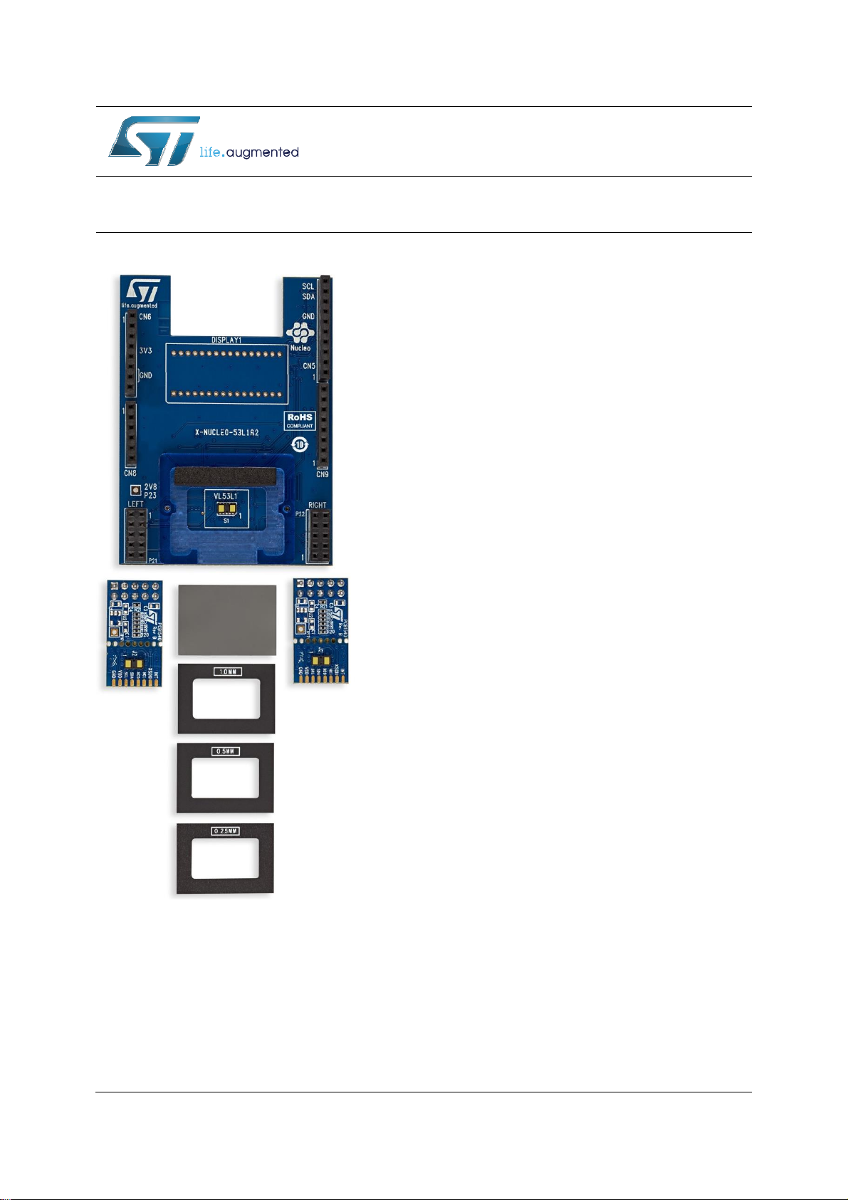
ST X-NUCLEO-53L1A2 User manual

Detailed Quick
Start Guide
Getting started with X-NUCLEO-53L1A2 ranging sensor with multi
target detection expansion board based on VL53L1 for STM32
Introduction
This document provides detailed hardware information on
the X-NUCLEO-53L1A2 expansionboard.This expansion
board is compatible with the STM32 Nucleo family and the
Arduino™electronic boards. It is designed around the
VL53L1 ranging sensor with multi target detection and is
based on the ST patented FlightSense™ technology.
To allow the user to validate the VL53L1 in an environment
as close as possible to its final application, the X-NUCLEO-
53L1A2 expansion board is delivered with a holder in which
three different height spacers of 0.25, 0.5, and 1 mm can be
fitted with the cover glass above the spacer. The height
spacers are used to simulate different air gap distances
between the VL53L1 sensor and the cover glass.
The X-NUCLEO-53L1A2expansion board is delivered with
two VL53L1 breakout boards.
Figure 1. X-NUCLEO-53L1A2expansion board,
spacers, cover glass, and
breakout boards
May 2020 1/17
www.st.com

Contents
Contents
1 Overview . . . . . . . . . . . . . . . . . . . . . . . . . . . . . . . . . . . . . . . . . . . . . . . . . . 3
2 Document references . . . . . . . . . . . . . . . . . . . . . . . . . . . . . . . . . . . . . . . . 3
3 X-NUCLEO-53L1A2 expansion board . . . . . . . . . . . . . . . . . . . . . . . . . . . 4
3.1 Overview . . . . . . . . . . . . . . . . . . . . . . . . . . . . . . . . . . . . . . . . . . . . . . . . . . 4
3.2 Electrical schematic and list of materials . . . . . . . . . . . . . . . . . . . . . . . . . . 8
3.2.1 Electrical schematic . ... . . ........... . . . . . . . .... . . ...... . . ... 8
3.2.2 List of materials . . . . ... . . ........... . . . . . . . .... . . ...... . . ... 9
3.3 Solder drop configurations . . . . . . . . . . . . . . . . . . . . . . . . . . . . . . . . . . . . 10
3.4 Integrated device pinning . . . . . . . . . . . . . . . . . . . . . . . . . . . . . . . . . . . . . 12
4 VL53L1 breakout board . . . . . . . . . . . . . . . . . . . . . . . . . . . . . . . . . . . 13
5 Safety . . . . . . . . . . . . . . . . . . . . . . . . . . . . . . . . . . . . . . . . . . . . . . . . . . . . 15
5.1 Electrostaticprecaution . . . . . . . . . . . . . . . . . . . . . . . . . . . . . . . . . . . . . . 15
5.2 Laser considerations . . . . . . . . . . . . . . . . . . . . . . . . . . . . . . . . . . . . . . . . 15
6 Revision history . . . . . . . . . . . . . . . . . . . . . . . . . . . . . . . . . . . . . . . . . . . 16
2/17

Overview
1 Overview
The X-NUCLEO-53L1A2expansion board features the VL53L1 ranging sensor, based on
ST’s FlightSense™, Time-of-Flight (ToF) technology.
It is compatible with the STM32 Nucleo development board family, and with the Arduino
UNO R3 connector layout.
Several ST expansion boards can be stacked through the Arduino connectors, which
allows, for example, the development of VL53L1 applications with Bluetooth or Wi-Fi
interfaces.
The X-NUCLEO-53L1A2expansion board is delivered with:
•
Three spacers of 0.25, 0.5, and 1 mm height, used to simulate different air gaps
between the VL53L1 and the cover glass.
•
Two cover windows to simulate the integration of the VL53L1 into the customer’sfinal
product.
•
Two VL53L1 breakout boards which can be plugged onto the X-NUCLEO-53L1A2
expansion board or connected through flying wires to the X-NUCLEO-53L1A2
expansion board.
•
Two 10-pinconnectors to enable the customerto connect the two breakout boards onto
the X-NUCLEO-53L1A2expansion board.
Note: The VL53L1 is delivered with a liner to prevent potential foreign material from penetrating
inside the module holes during the assembly process. This liner must be removed at the
latest possible step during final assembly, before module calibration.
Table 1. Ordering information
Order code
Desc
ription
X-NUCLEO-53L1A2
STM32 Nucleo expansion board - spacers and glass - two breakout boards
2 Document references
Table 2. Document references
Desc
ription
D
ocID
VL53L1 datasheet
DS11786
X-NUCLEO-53L1A2 data brief
DB4214
P-NUCLEO-53L1A2 data brief
DBxxxx
X-CUBE-53L1A2 data brief
DB4252
3/17

X-NUCLEO-53L1A2 expansion board
3 X-NUCLEO-53L1A2 expansion board
This section describes the X-NUCLEO-53L1A2expansion board features and provides
useful information for understanding the electrical characteristics.
Figure 2. X-NUCLEO-53L1A2 expansion board schematic diagram
X-NUCLEO-53L1A2 expansion board
VL53L1 VL53L1 .
VL53L1
3.1 Overview
The board allows the user to test the VL53L1functionality,to program it and to understand
how to develop an application using the VL53L1. It integrates:
•
2.8 V regulator to supply the VL53L1
•
Level translators to adapt the I/O level to the main board of the microcontroller
•
Arduino UNO R3 connectors
•
Optional VL53L1 breakout board connectors
•
Solder drops to allow different configurations of the expansion board
4/17

X-NUCLEO-53L1A2 expansion board
It is fundamental to program a microcontroller to control the VL53L1 through the I2C bus.
The application software and an examples of the C-ANSI source code are available on
www.st.com
The X-NUCLEO-53L1A2expansion board and STM32 Nucleo development board are
connected through the Arduino™ UNO R3 connectors CN5, CN6, CN8, and CN9 as shown
in Figure 3 and as described in Table 3 and Table 4.
The X-NUCLEO-53L1A2must be plugged onto the STM32 Nucleo development board
through the Arduino™UNO R3 connectors.
Figure 3. X-NUCLEO-53L1A2 expansion board connector layout
5/17

X-NUCLEO-53L1A2 expansion board
Table 3. Left Arduino connector
CN
nu
mber
VL
53L1
bo
ard
Pin
number
Pin
name
MCU
pin
X-NUCLEO-53L1A2
expansion board function
CN6 power
1
NC
NC
2
NC
IOREF
Not used
3
NC
RESET
Power
4
3V3
3V3
3.3 V supply
5
NC
5
V
Not used
Gnd
6
Gnd
G
nd
Gnd
Gnd
7
Gnd
G
nd
8
NC
VI
N
Not used
CN8 analog
1
NC
PA
0
2
NC
PA
1
GPIO1
3
INT
P
A4
Interrupt signal from VL53L1
on board soldered device
4
NC
PB0
Not used
GPIO1
5
INT*
PC1 (1)
By default not used, interrupt
signal from VL53L1 on board
soldered device
6
NC
P
C0
Not used
1. Depends on STM32 Nucleo board solder bridges, see details in Section 3.3: Solder drop configurations.
These interrupt signals are duplicated, but not used. This offers hardware connection flexibility in case of
conflict on the MCU interface management when the expansion board is used superimposed with other
expansion boards. In this case, remove the solder drop from the used interrupt and instead, fit the solder
drop in “NC”.
6/17

X-NUCLEO-53L1A2 expansion board
Table 4. Right Arduino connector
CN
nu
mber
VL
53L1
bo
ard
Pin
number
Pin
name
MCU
pin
X-NUCLEO-53L1 expansion
board function
CN5 digital
SCL
10
D15
PB8
I2C1_SCL
SDA
9
D14
PB9
I2C1_SDA
8
NC
AVDD
Not used
Gnd
7
Gnd
Gnd
Gnd
6
INT_L
PA5
Not used
5
NC
PA6
4
NC
PA7
3
NC
PB6
GPIO1_L
2
INT_L*
PC7
By default not used, interrupt signal
from optional VL53L1 left breakout
board (1)
GPIO1_L
1
INT_L
PA9
By default not used, interrupt signal
from optional VL53L1 left breakout
board (1)
CN9 digital
8
NC
PA8
Not used
7
NC
PB10
6
NC
PB4
GPIO1_R
5
INT_R*
PB5
By default not used, interrupt signal
from optional VL53L1 right breakout
board (1)
4
NC
PB3
Not used
GPIO1_R
3
INT_R
PA10
By default not used, interrupt signal
from optional VL53L1 right breakout
board (1)
2
NC
PA2
Not used
1
NC
PA3
1. These interrupt signals are duplicated, but not used by default. This offers hardware connection of the
breakout board VL53L1 interrupt signals and flexibility in case of conflict on the MCU interface
management when the expansion board is used superimposed with other expansion boards. In this case,
select, through a solder drop, the MCU port which is free.
7/17

X-NUCLEO-53L1A2 expansion board
3.2 Electrical schematic and list of materials
3.2.1 Electrical schematic
Figure 4. X-NUCLEO-53L1A2 expansion board schematic
VL53L1
9/53/1
VL53L1 application
VL53L1
*CanbeNCorgrounded
8/17

X-NUCLEO-53L1A2 expansion board
3.2.2 List of materials
Table 5. List of
materials
Components
Value
Reference
Supplier
C
o
mments
VL53L1 application
C1, C3
100 nF
X5R
Supply voltage decoupling
C2
4.7 µF
X5R - 6.3 V
R1
47 k
Interrupt output pull up
R2
47 k
Reset input pull up
R66, R67
4.7 k
SDA and SCL line pull up at 2.8 V
S1
VL53L1
ST
ToF ranging sensor
VL53L1breakout board interfaces
R20
47 k
Left breakout board interrupt
output pull up
R21
47 k
Left breakout board reset input
pull up
R22
47 k
Right breakout board reset input
pull up
R23
47 k
Right breakout board interrupt
output pull up
2.8 V regulator application
C8
10 µF
X5R - 6.3 V
Output voltage decoupling
C9
10 µF
X5R - 6.3 V
Input voltage decoupling
R35
49.9 k
Feedback resistor bridge to set
the output voltage to 2.8 V
R43
20 k
U20
LD39050PUR
ST
Output programmable regulator
Level translator application
C4, C6, C11
100 nF
2.8 V decoupling capacitor
C5, C7, C13
100 nF
3.3 V decoupling capacitor
C12
1 µF
X5R - 6.3V
R68, R69
4.7 k
SDA and SCL line pull up at 3.3 V
U3, U9
TXS0108PWR
TI
For all signals except I2C
interface
U24
ST2329AQTR
ST
For I2C interface
Add-on feature
C10
100 nF
Supply decoupling capacitor
R45
4.7 k
Push-button pull up
R46
1 k
Output pull up
R60
0
Delay time setting (def = 10 ms)
9/17

X-NUCLEO-53L1A2 expansion board
Table 5. List of materials (continued)
Components
Value
Reference
Supplier
C
o
mments
PB1
Push button
U22
TPS3838K33
TI
Supervisory circuit
GPIO expander
C14, C15
100 nF
Supply decoupling capacitor
3.3 Solder drop configurations
Solder drops allow the following configurations of the X-NUCLEO-53L1A2expansion board:
•
If the developer wants to make an application with several expansion boards stacked
and there is:
–conflict with the microcontroller port allocation, the GPIO1 can be output on the
CN8/A4 (U17 fitted) of the Arduino connector. The default configuration is that
GPIO1 is output on the CN8/A2 (U14 fitted) of the Arduino connector.
–conflict on the I2C addresses, the addresses of the STMPE1600 can be modified
(the default addresses A2, A1, A0, 000, and 001).
•
If the developer wants to connect breakout boards (see Figure 5) to the X-NUCLEO-
53L1A2 expansion board:
–the VL53L1 interrupt of the left breakout board can be output on the CN5/D9
(U10 fitted) or CN5/D8 (U11 fitted) of the Arduino connector. By default, the U10
and U11 are not fitted.
–the VL53L1 interrupt of the right breakout board can be output on the CN9/D4
(U15 fitted) or CN9/D2 (U18 fitted) of the Arduino connector. By default, the U15
and U18 are not fitted.
–the VL53L1 interrupts of the left and right breakout boards, GPIO1_L and
GPIO1_R, can be shared with the VL53L1 interrupt on the main board, GPIO1,
by fitting U7 and U8 solder drops. By default U7 and U8 are not fitted.
10/17

X-NUCLE0-53L1A2
expansion
board
Figure 5. Interrupt
configurations
GPI01
configuration
GPI01 L and GPI01 R
shared-with
GPI01
-
11/17

X-NUCLEO-53L1A2 expansion board
3.4 Integrated device pinning
Figure 6. Integrated device pinning
12/17

VL53L1 breakout board
4 VL53L1 breakout board
The VL53L1 breakout boards are supplied at 2.8 V by the regulator present on the
X-NUCLEO-53L1A2expansion board.
Figure 7. VL53L1 breakout board schematic
VL53L1
VL53L1 breakout
board
VL53L1 mini PCB
VL53L1
The VL53L1 breakout boards can be directly plugged onto the X-NUCLEO-53L1A2
expansionboard through thetwo 10-pin connectorsor connectedto the boardthroughflying
leads.
When connected through flying leads, developers should break off the mini PCB from the
breakout board, and use only the “VL53L1 mini PCB” which because of its small size, is
easier to integrate into customers devices.
13/17

VL53L1 breakout
board
Figure 8. VL53L1 mini PCB flying lead connection to X-NUCLEO-53L1A2 expansion board
14/17

Safety
5 Safety
5.1 Electrostatic precaution
Figure 9. Electrostatic logo
The user should exercise electrostatic precautions, including using ground straps when
using the X-NUCLEO-53L1A2expansion board. Failure to prevent electrostatic discharge
could damage the device.
5.2 Laser considerations
The VL53L1 contains a laser emitter and correspondingdrive circuitry. The laser output is
designed to remain within Class 1 laser safety limits under all reasonably foreseeable
conditions including single faults, in compliance with the IEC 60825-1:2014 (third edition).
The laser output remains within Class 1 limits as long as
STMicroelectronic’s
recommended
device settings are used and the operating conditions specified in the datasheet are
respected. The laser output power must not be increased by any means and no optics
should be used with the intention of focusing the laser beam.
Figure 10. Class 1 laser product
label
15/17

Revision history
6 Revision history
Table 6. Document revision history
Date
Revision
Changes
01-07-2020
1
Initial release
16/17

IMPORTANT NOTICE –PLEASE READ CARE
FULLY
STMicroelectronics NV and its subsidiaries (“ST”) reserve the right to make changes, corrections, enhancements, modifications, and
improvements to ST products and/or to this document at any time without notice. Purchasers should obtain the latest relevant information on
ST products before placing orders. ST products are sold pursuant to ST’s terms and conditions of sale in place at the time of order
acknowledgement.
Purchasers are solely responsible for the choice, selection, and use of STproducts and ST assumes no liability for application assistance or
the design of Purchasers’products.
No license, express or implied, to any intellectual property right is granted by ST herein.
Resale of ST products with provisions different from the information set forth herein shall void any warranty granted by ST for such product.
ST and the ST logo are trademarks of ST. All other product or service names are the property of their respective owners.
Information in this document supersedes and replaces information previously supplied in any prior versions of this document.
© 2018 STMicroelectronics –All rights reserved
17/17
This manual suits for next models
1
Table of contents
Other ST Accessories manuals

ST
ST LPS22HB Installation and operating instructions

ST
ST STEVAL-IOD04KT1 User manual

ST
ST VL53L4CX User manual

ST
ST VL53L3CX User manual

ST
ST VL6180 User manual

ST
ST UM2884 User manual

ST
ST X-NUCLEO-53L3A2 User manual

ST
ST VL6180X Installation and operating instructions

ST
ST VL53L1X API User manual

ST
ST LIS331AL User manual