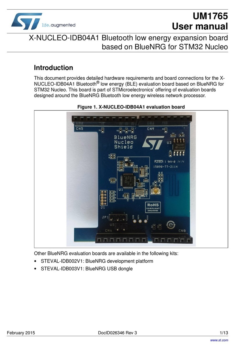
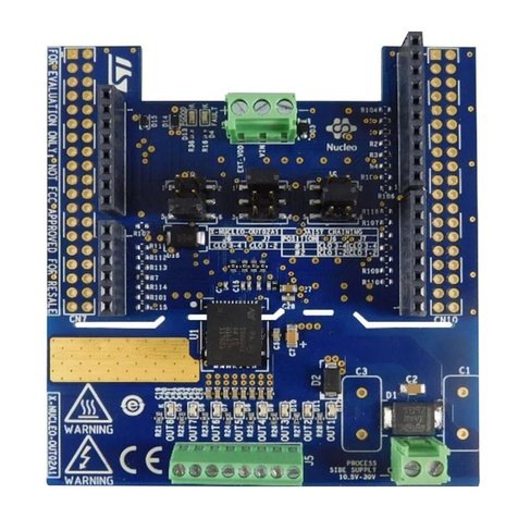
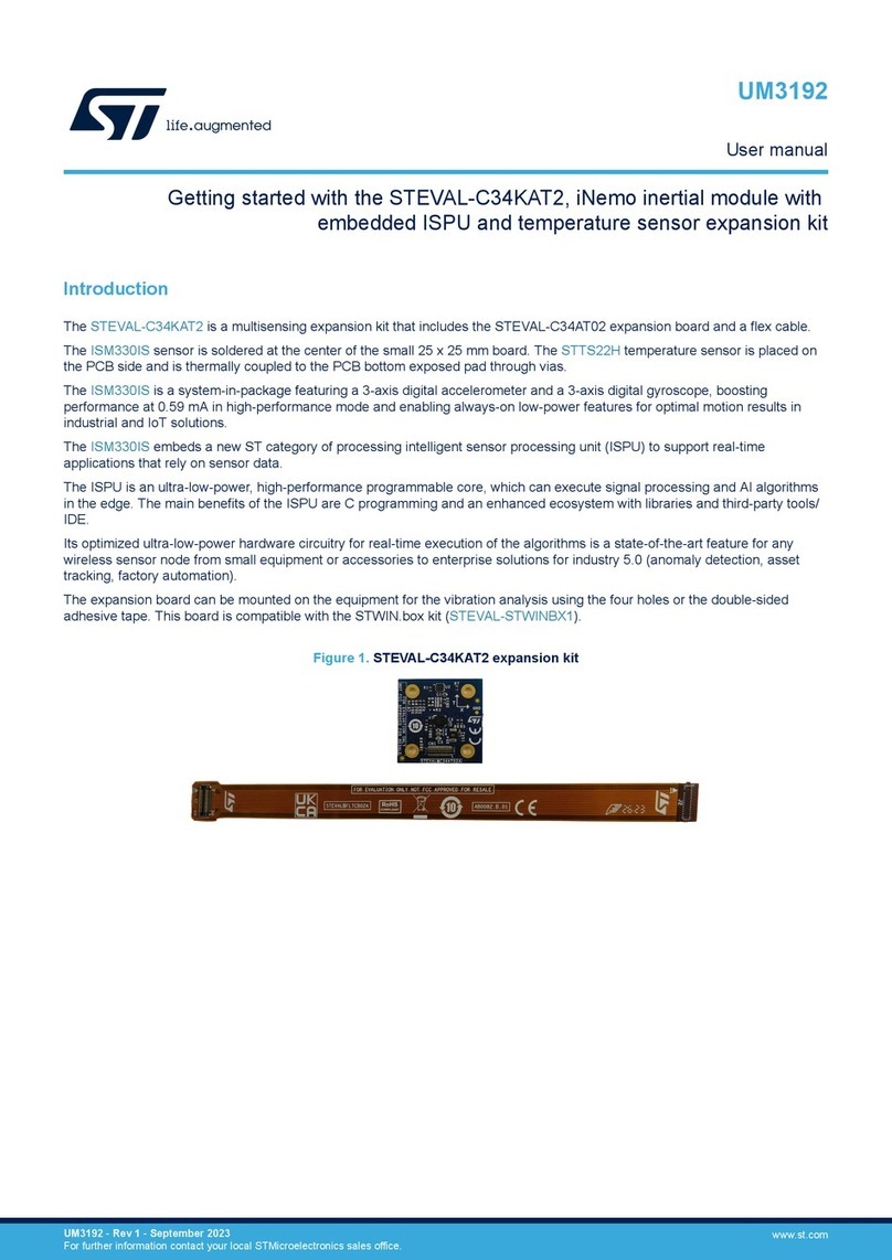
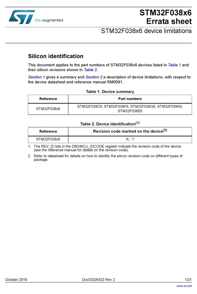
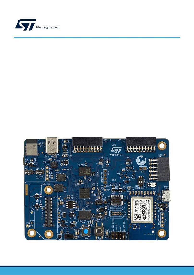
ST B-WB1M-WPAN1 User manual

Introduction
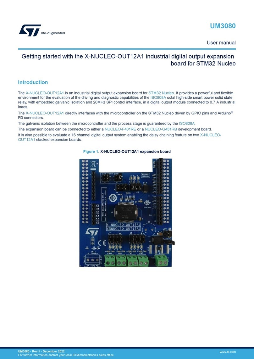
The B-WB1M-WPAN1 STM32WB connectivity expansion board provides an affordable and flexible way for users to try out new
concepts and build prototypes with the STM32WB series STM32WB1MMC microcontroller module.
The B-WB1M-WPAN1 product requires a separate probe for programming and debugging. The STLINK-V3SET debugger can
be connected through a MIPI10/STDC14 cable.
The B-WB1M-WPAN1 STM32WB connectivity expansion board is provided with a USB Type-C® connector (for power only) on
an add-on STMod+ adapter board.
The B-WB1M-WPAN1 product is provided with the STM32WB comprehensive software HAL library and various packaged
software examples available with the STM32CubeWB MCU Package.
Figure 1. B-WB1M-WPAN1 main board (top view)
Figure 2. B-WB1M-WPAN1 main board (bottom view)
Pictures are not contractual.
STM32WB connectivity expansion board
UM3200
User manual
UM3200 - Rev 1 - November 2023
For further information contact your local STMicroelectronics sales office. www.st.com

1 Features
• STM32WB connectivity expansion board embedding an STM32WB1MMC module including:
–Ultra‑low‑power STM32WB15CCY dual‑core Arm® Cortex®‑M4/M0+, Bluetooth® Low Energy 5.4,
AES‑256, featuring 320 Kbytes of flash memory and 48 Kbytes of SRAM in a WLCSP49 package
– RF transceiver multistandard radio Bluetooth® Low Energy, compliant with Bluetooth® specification
5.4 with 1 and 2 Mbit/s transfer rates
• 256‑Kbit serial I2C bus EEPROM
• MEMS sensors from STMicroelectronics:
– Integrated high-accuracy temperature sensor
– 3D accelerometer and 3D gyroscope
• User LED
• User and reset push-buttons
• Board connectors:
–MIPI® debug
– STMod+
–USB Type-C® for power only on add‑on STMod+ adapter board
• Flexible power supply options: external sources, or USB VBUS from the add‑on board
• Comprehensive free software libraries and examples available with the STM32CubeWB MCU Package
• Support of a wide choice of Integrated Development Environments (IDEs) including IAR Embedded
Workbench®, MDK-ARM, and STM32CubeIDE
Note: Arm is a registered trademark of Arm Limited (or its subsidiaries) in the US and/or elsewhere.
UM3200
Features
UM3200 - Rev 1 page 2/38

2 Ordering information
To order the B-WB1M-WPAN1 STM32WB connectivity expansion board, refer to Table 1. Additional information is
available from the datasheet and reference manual of the target microcontroller.
Table 1. List of available products
Order code Board reference Target STM32
B-WB1M-WPAN1 • MB1868(1)
• MB1880(2) STM32WB1MMCH6TR
1. Expansion board
2. STMod+ adapter board
2.1 Codification
The meaning of the codification is explained in Table 2.
Table 2. Codification explanation
B-XXYY-ZZZZT Description Example: B-WB1M-WPAN1
B Expansion board Connectivity expansion board
XX MCU series in STM32 32-bit Arm Cortex MCUs STM32WB series
YY MCU product line in the series STM32WB1M line
ZZZZ Wireless network Wireless personal area network based
on Bluetooth® Low Energy 5.4 certified
T Sequential number First WPAN connectivity expansion
board
UM3200
Ordering information
UM3200 - Rev 1 page 3/38

3 Development environment
The B-WB1M-WPAN1 STM32WB connectivity expansion board runs with the STM32WB1MMC module including
the STM32WB15CCY 32-bit microcontroller based on the dual‑core Arm® Cortex®‑M4/M0+ processor.
Note: Arm is a registered trademark of Arm Limited (or its subsidiaries) in the US and/or elsewhere.
3.1 System requirements
•Multi‑OS support: Windows® 10, Linux® 64-bit, or macOS®
•USB Type-A or USB Type-C® to USB Type-C® cable
Note: macOS® is a trademark of Apple Inc., registered in the U.S. and other countries and regions.
Linux® is a registered trademark of Linus Torvalds.
Windows is a trademark of the Microsoft group of companies.
3.2 Development toolchains
•IAR Systems® - IAR Embedded Workbench®(1)
• Keil® - MDK-ARM(1)
• STMicroelectronics - STM32CubeIDE
1. On Windows® only.
3.3 Demonstration software
The demonstration software, included in the STM32Cube MCU Package corresponding to the on-board
microcontroller, is preloaded in the STM32 flash memory for easy demonstration of the device peripherals in
standalone mode. The latest versions of the demonstration source code and associated documentation can be
downloaded from www.st.com.
UM3200
Development environment
UM3200 - Rev 1 page 4/38

4 Conventions
Table 3 provides the conventions used for the ON and OFF settings in the present document.
Table 3. ON/OFF convention
Convention Definition
Jumper JPx ON Jumper fitted
Jumper JPx OFF Jumper not fitted
Jumper JPx [1-2] Jumper fitted between Pin 1 and Pin 2
Solder bridge SBx ON SBx connections closed by 0 Ω resistor
Solder bridge SBx OFF SBx connections left open
Resistor Rx ON Resistor soldered
Resistor Rx OFF Resistor not soldered
Capacitor Cx ON Capacitor soldered
Capacitor Cx OFF Capacitor not soldered
UM3200
Conventions
UM3200 - Rev 1 page 5/38

5 Quick start
The B-WB1M-WPAN1 STM32WB connectivity expansion board is an easy-to-use and low-cost development kit
used to evaluate and start development quickly with an STM32WB1MMC module. Before installing and using the
product, accept the evaluation product license agreement from the www.st.com/epla webpage. For more
information on the B-WB1M-WPAN1 STM32WB connectivity expansion board and demonstration software, visit
www.st.com.
5.1 Getting started
Follow the sequence below to configure the B-WB1M-WPAN1 STM32WB connectivity expansion board and
launch the demonstration application (refer to Figure 4 for component location):
1. Check jumper positions on board, JP1 (IDD) ON. The default jumper position on the board is explained in
Table 4.
2. Choose one of the several possibilities to supply the B-WB1M-WPAN1 STM32WB connectivity expansion
board (MB1868) with power. For example, connect a supply cable to CN4 to supply the board with an
external 5 V supply source (E5V).
3. Press on the reset button (B2) of the B-WB1M-WPAN1 STM32WB connectivity expansion board (MB1868)
and the demonstration starts.
4. This demonstration application software is available on the www.st.com website.
Table 4. Jumper default configuration
Jumper Definition Position(1) Comment
JP1 IDD ON For STM32WB1MMC current
measurements (RF part)
1. The default jumper state is shown in bold.
UM3200
Quick start
UM3200 - Rev 1 page 6/38

6 Hardware layout and configuration
6.1 Connectivity expansion board (MB1868)
The CEB (connectivity expansion board) MB1868 is designed around the STM32WB1MMC module, which
includes an STM32WB15CCY microcontroller. Figure 3 shows the connections between the STM32WB1MMC
module and its peripherals, push-buttons, LEDs, USB, and sensors. Figure 4 and Figure 5 show the location of
these features on the CEB MB1868. The mechanical dimensions of the board are shown in Figure 6.
Figure 3. MB1868 hardware block diagram
DT59181V1
I2C
SPI
VCP SWD
GPIO
STM32WB15CCY
XTAL 32
MHz
XTAL 32
kHz SMPS
IPD Antenna
matching
Internal
antenna
STM32WB1MMC
(CN1)
(U4)
DEBUG
(CN3)
STMod+ connector
Temperature
sensor
(U1)
Accelerometer
Gyroscope
(U2)
EEPROM
(U3)
User
button
(B1)
User
blue LED
(LD1)
Reset
button
5V_PWR
green LED
(B2)
(LD2)
E5V
E3V3
(CN4) (CN5)
UM3200
Hardware layout and configuration
UM3200 - Rev 1 page 7/38

6.1.1 MB1868 layout
Figure 4. MB1868 top layout
DT59182V1
Product sticker
STM32WB1MMC (U4)
SMA (CN2)
USER button (B1)
RESET button (B2)
USER LED (LD1)
5V_PWR LED (LD2)
IDD jumper for current
measurement (JP1)
STDC14 programming and
debug connector (CN3)
E3V3 connector supply (CN5)
E5V connector supply (CN4)
Temperature sensor (U1)
3D accelerometer
and 3D gyroscope (U2)
I2C EEPROM (U3)
STMod+
connector
(CN1)
Figure 5. MB1868 bottom layout
DT59183V1
STMod+
connector
(CN1)
Board sticker
UM3200
Connectivity expansion board (MB1868)
UM3200 - Rev 1 page 8/38

6.1.2 MB1868 mechanical drawing
Figure 6. MB1868 mechanical drawing (in millimeters)
UM3200
Connectivity expansion board (MB1868)
UM3200 - Rev 1 page 9/38

6.2 STMod+ adapter board (MB1880)
The MB1880 STMod+ adapter board is a very simple board that allows the MB1868 connectivity expansion board
to become a host with the add-on STMod+ connectors (female).
Figure 7 shows the basic hardware block diagram. Figure 1 and Figure 2 show the location of the main
components of the MB1880 board. The mechanical dimensions of the board are shown in Figure 10.
Figure 7. MB1880 basic hardware block diagram
DT59131V1
JP1
STMod+
connector
(CN2)
STMod+
connector
(CN3)
USB C
(CN1)
JP2
6.2.1 MB1880 layout
Figure 8. MB1880 top layout
DT59132V1
STMod+
connector
(CN2)
Jumper
(JP1)
5V test point
(TP2)
GND test point
(TP1)
Jumper
(JP2)
STMod+
connector
(CN3)
ESDA7P60-1U1M
ESD protection
(U1)
USB Type-C®
connector
(CN1)
UM3200
STMod+ adapter board (MB1880)
UM3200 - Rev 1 page 10/38

Figure 9. MB1880 bottom layout
DT59133V1
STMod+
connector
(CN3)
Board sticker
EMS sticker
(reserved for EMS)
STMod+
connector
(CN2)
6.2.2 MB1880 mechanical drawing
Figure 10. MB1880 mechanical drawing (in millimeters)
UM3200
STMod+ adapter board (MB1880)
UM3200 - Rev 1 page 11/38

6.3 Power supply
Four different sources can provide the power supply:
• An external E5V 5 V power supply connected to CN4 (preferred solution)
• An external E3V3 3.3 V power supply connected to CN5
• 5 V via the STMod+ adapter board (MB1880) supplied through the USB Type-C® connector (CN1)
• 5 V via the STMod+ adapter board (MB1880) supplied through a host connected to CN3
Figure 11. CEB MB1868 power tree
DT59186V1
E5V connector (CN4)
E5V
SB21 ON
E3V3 connector (CN5)
SB20 OFF
I2C EEPROM
(U3)
3V3
LDO (U8)
3V3
3V3
JP1
(current
measurement)
STM32WB1MMC (U4)
VDD
VDDA
VBAT
STMod+ connector (CN1)
5V
5V
5V
3V3
STDC14
programming and
debug connector (CN3)
3V3
SB19 ON
3V3 3V3_MEMS
Sensors:
-3D accelerometer and 3D
gyroscope (U4)
- Temperature sensor (U1)
In case an external voltage supply on E5V is used to power the connectivity expansion board MB1868, this E5V
power source must comply with the EN‑60950-1: 2006+A11/2009 standard and must be safety extra low voltage
(SELV) with limited power capability.
UM3200
Power supply
UM3200 - Rev 1 page 12/38

6.3.1 Power supply input E5V connector (default setting)
The CEB MB1868 can be powered from the E5V connector (CN4) by either:
• Plugging an external voltage supply (from 3.6 up to 5.5 V)
• Plugging a 3.7 V battery pack
Refer to Table 5. This is the default setting.
Table 5. External power source E5V
Input power name Connector pins Voltage range Maximum current
E5V MB1868 - CN4 pin 1 3.6 to 5.5 V 500 mA
Make sure you supply the board with the correct power when using CN4. CN4 pin 1 is the E5V supply and pin 2 is
the GND, as shown in Figure 12.
Figure 12. E5V and GND pins on CN4
DT59188V1
E5VGND
UM3200
Power supply
UM3200 - Rev 1 page 13/38

6.3.2 Power via STMod+ adapter board (MB1880) supplied through a USB Type-C® connector
The CEB MB1868 can be powered by 5V coming from the USB Type-C® connector of the STMod+ adapter board
(MB1880). This USB Type-C® connector can be connected to:
• A PC through a USB cable
• A USB charger
This is displayed in Table 6 and Figure 13.
Figure 13. Power supply from 5V via STMod+ adapter board (MB1880) connected through a USB
connector
DT59189V1
Table 6. External power source 5V
Input power name Connector pins Voltage range Maximum current
5V MB1880 - CN1 5 V 500 mA
6.3.3 Power via STMod+ adapter board (MB1880) supplied through a host
The CEB MB1868 can be powered by 5V coming from the second STMod+ connector of the STMod+ adapter
board (MB1880). This STMod+ connector can be connected to a host.
This is displayed in Figure 14.
Figure 14. Power supply input from 5V via STMod+ adapter board (MB1880) connected to a host
DT59190V1
UM3200
Power supply
UM3200 - Rev 1 page 14/38

6.3.4 Power supply input E3V3 connector
The CEB MB1868 can be powered by the E3V3 connector (CN5) by plugging an external E3V3 voltage supply
(up to 3.6 V).
Refer to Table 7.
Table 7. External power source E3V3
Input power name Connector pins Voltage range Maximum current
E3V3 MB1868 - CN5 pin 1 Up to 3.6 V 500 mA
Make sure to supply the card with the correct power when using CN5.
A 2‑pin header must be used with CN5.
CN5 pin 1 is the E3V3 supply and pin 2 is the GND, as shown in Figure 15.
Figure 15. E3V3 and GND pins on CN5
DT59192V1
GND E3V3
UM3200
Power supply
UM3200 - Rev 1 page 15/38

6.4 Board functions
6.4.1 LEDs
User LED (LD1)
This blue LED is a user LED connected to the STM32WB1MMC module I/O PB0. To light the LD1 LED, a HIGH
logic state must be written in the corresponding GPIO PB0.
5V_PWR LED (LD2)
This green LED indicates that the CEB MB1868 is powered, and 5V power is available at the input of the 3V3
regulator (U8) to provide the 3.3 V necessary to supply the STM32WB1MMC module.
6.4.2 Push-buttons
User button (B1)
This user button is connected to the STM32WB1MMC module I/O PB1.
Reset button (B2)
This push-button is connected to NRST and is used to reset the STM32WB1MMC module.
6.4.3 Current consumption measurement (IDD)
Jumper JP1 labeled IDD, is used to measure the STM32WB1MMC module power consumption by removing the
jumper and by connecting an ammeter. Its location in the power structure is shown in Figure 11.
1. JP1 ON. STM32WB1MMC is powered with the 3V3 voltage (default).
2. JP1 OFF. An ammeter must be connected to measure the STM32WB1MMC current. If there is no ammeter, the
STM32WB1MMC module is not powered.
UM3200
Board functions
UM3200 - Rev 1 page 16/38

6.5 Solder bridges
There are 21 solder bridges on the MB1868, and there is one solder bridge on the MB1880 board.
On MB1868, all 21 solder bridges are located on the bottom side of the CEB MB1868.
All the solder bridges present on the CEB MB1868 are used to configure several I/Os and power supply pins for
compatibility of features and pinout with the supported target STM32WB1MMC module.
Table 8. Solder bridge configuration on MB1868
Solder bridge control Solder bridge
(SB)
State(
1) Description(1)
STMOD+_UART1_RTS
(PA12)
SB1
(SB1 and SB2
are exclusive.)
ON UART1_RTS connected to pin 1 of the STMod+ connector
OFF UART1_RTS not connected to pin 1 of the STMod+ connector
STMOD+_SPI1_NSS
(PA4)
SB2
(SB1 and SB2
are exclusive.)
ON SPI1_NSS connected to pin 1 of the STMod+ connector
OFF SPI1_NSS not connected to pin 1 of the STMod+ connector
STMOD+_UART1_RX
(PA10)
SB3
(SB3 and SB4
are exclusive.)
ON UART1_RX connected to pin 2 of the STMod+ connector
OFF UART1_RX not connected to pin 2 of the STMod+ connector
STMOD+_SPI1_MOSIP
(PA7)
SB4
(SB3 and SB4
are exclusive.)
ON SPI1_MOSIP connected to pin 2 of the STMod+ connector
OFF SPI1_MOSIP not connected to pin 2 of the STMod+ connector
STMod+ connector pin 12
SB5 ON NRST connected to pin 12 of the STMod+ connector
OFF NRST not connected to pin 12 of the STMod+ connector
SB7 ON PA1 connected to pin 12 of the STMod+ connector
OFF PA1 not connected to pin 12 of the STMod+ connector
STMOD+_UART1_TX
(PA9)
SB6
(SB6 and SB8
are exclusive.)
ON UART1_TX connected to pin 3 of the STMod+ connector
OFF UART1_TX not connected to pin 3 of the STMod+ connector
STMOD+_SPI1_MISOP
(PA6)
SB8
(SB6 and SB8
are exclusive.)
ON SPI1_MISOP connected to pin 3 of the STMod+ connector
OFF SPI1_MISOP not connected to pin 3 of the STMod+ connector
STMOD+_UART1_CTS
(PA11)
SB9
(SB9 and
SB10 are
exclusive.)
ON UART1_CTS connected to pin 4 of the STMod+ connector
OFF UART1_CTS not connected to pin 4 of the STMod+ connector
STMOD+_SPI1_SCK
(PA5)
SB10
(SB9 and
SB10 are
exclusive.)
ON SPI1_SCK connected to pin 4 of the STMod+ connector
OFF SPI1_SCK is not connected to pin 4 of the STMod+ connector
I2C2_SCL (PB6) SB11 ON I2C2_SCL connected to pin 7 of the STMod+
I2C2_SDA (PB7) SB12 ON I2C2_SDA connected to pin 10 of the STMod+
I2C EEPROM chip enable input
(E1)
SB13
(SB13 and
SB14 are
exclusive.)
ON Chip enable input (E1) set to 3V3
OFF Chip enable input (E1) not set to 3V3, so should be set to GND
with SB14
UM3200
Solder bridges
UM3200 - Rev 1 page 17/38

Solder bridge control Solder bridge
(SB)
State(
1) Description(1)
I2C EEPROM chip enable input
(E1)
SB14
(SB13 and
SB14 are
exclusive.)
ON Chip enable input (E1) set to GND
OFF Chip enable input (E1) not set to GND, so should be set to
3V3 with SB13
I2C EEPROM chip enable input
(E2)
SB15
(SB15 and
SB16 are
exclusive.)
ON Chip enable input (E2) set to 3V3
OFF Chip enable input (E2) not set to 3V3, so should be set to GND
with SB16
I2C EEPROM chip enable input
(E2)
SB16
(SB15 and
SB16 are
exclusive.)
ON Chip enable input (E2) set to GND
OFF Chip enable input (E2) not set to GND, so should be set to
3V3 with SB15
VCP_TX (PA9) SB17 ON PA9 connected to VCP_TX (STDC14 connector)
OFF PA9 not connected to VCP_TX (STDC14 connector)
VCP_RX (PA10) SB18 ON PA10 connected to VCP_RX (STDC14 connector)
OFF PA10 not connected to VCP_RX (STDC14 connector)
3V3_MEMS SB19 ON 3V3_MEMS connected to 3V3.
OFF 3V3_MEMS not connected to 3V3.
E3V3 SB20 ON E3V3 connected to 3V3.
OFF E3V3 not connected to 3V3.
E5V SB21 ON E5V connected to 5V. Board supplied from CN4.
OFF E5V not connected to 5V.
1. The default SB state is in bold.
On MB1880, the solder bridge SB1 is located on the top side of the board.
Table 9. Solder bridge configuration on MB1880
Solder bridge control Solder bridge
(SB)
State(
1) Description(1)
5 V on VBUS SB1
ON 5 V voltage supply connected to the VBUS supply of the USB-
C® connector.
OFF 5 V voltage supply not connected to the VBUS supply of the USB-
C® connector.
1. The default SB state is in bold.
UM3200
Solder bridges
UM3200 - Rev 1 page 18/38

6.6 Jumpers
6.6.1 MB1868 jumper
The jumper JP1 labeled IDD, is used to measure the STM32WB1MMC module power consumption by removing
the jumper and by connecting an ammeter. Refer to Section 6.4.3.
6.6.2 MB1880 jumpers
The MB1880 board has two parallel jumpers as shown in Figure 1, Figure 2, and Figure 10. Set these jumpers in
positions that are consistent with the solder bridges on MB1868 as indicated in Table 10.
Table 10. Consistent JP (MB1880) and SB (MB1868) settings for SPI or UART functions
- JP1, JP2 SB1 SB2 SB3 SB4 SB6 SB8 SB9 SB10
SPI [2‑3] OFF ON OFF ON OFF ON OFF ON
UART [1‑2] ON OFF ON OFF ON OFF ON OFF
6.7 Embedded devices
6.7.1 I2C interface
Two B-WB1M-WPAN1 embedded sensors and the EEPROM are connected to the STM32WB1MMC module with
an I2C bus. The accelerometer/gyroscope, and temperature sensors are connected to the STM32WB1MMC I2C1
bus.
The address is a 7‑bit address with an additional read/write bit (HIGH for reading, LOW for writing). Table 11
describes the different addresses to read or write action for each component:
Table 11. I2C addresses
Device Action Address
Accelerometer-gyroscope sensor (U2) Read 1101 0101 (D5h)
Write 1101 0100 (D4h)
Temperature sensor (U1) Read 0111 1111 (7Fh)
Write 0111 1110 (7Eh)
U3 (EEPROM)
Memory array
Read 10101 101 (ADh)
Write 1010 1100 (ACh)
U3 (EEPROM)
Identification page
Read 1011 1101 (BDh)
Write 1011 1100 (BCh)
6.7.2 Temperature sensor
U1 is a device that measures ambient temperature. It is connected to the STM32WB1MMC through the I2C
interface.
6.7.3 3D accelerometer and 3D gyroscope (U2)
U2 is connected to STM32WB1MMC through the I2C interface.
UM3200
Jumpers
UM3200 - Rev 1 page 19/38

U2 is a system-in-package featuring a high‑performance 3D digital accelerometer and 3D digital gyroscope
tailored for Industry 4.0 applications.
Figure 16. 3D direction for acceleration and angular rate
Figure 17. 3D accelerometer and 3D gyroscope (U2) pin 1 location
DT59210V1
Pin 1
UM3200
Embedded devices
UM3200 - Rev 1 page 20/38
Table of contents
Other ST Computer Hardware manuals
Popular Computer Hardware manuals by other brands

ADS Technologies
ADS Technologies INSTANTHDTV PCI PTV380 - SOFTWARE GUIDE 1 Software guide

Cambricon
Cambricon MLU270-F Series user manual

Tews Technologies
Tews Technologies TVME201 user manual

Air Techniques
Air Techniques PERI-PRO III user manual

CanMore
CanMore Gplayer user manual

BenQ
BenQ QCast Mirror QP30 user manual