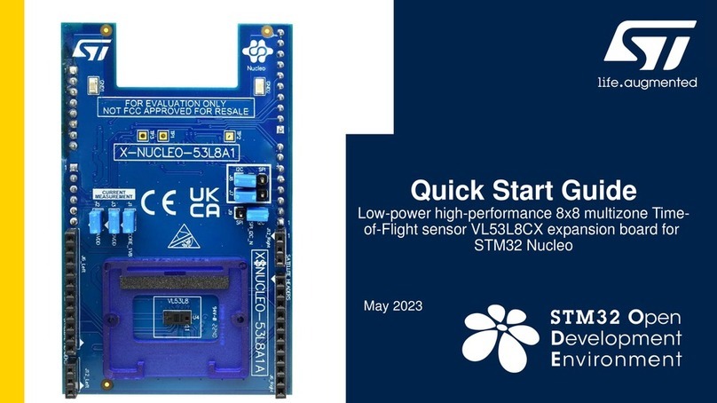
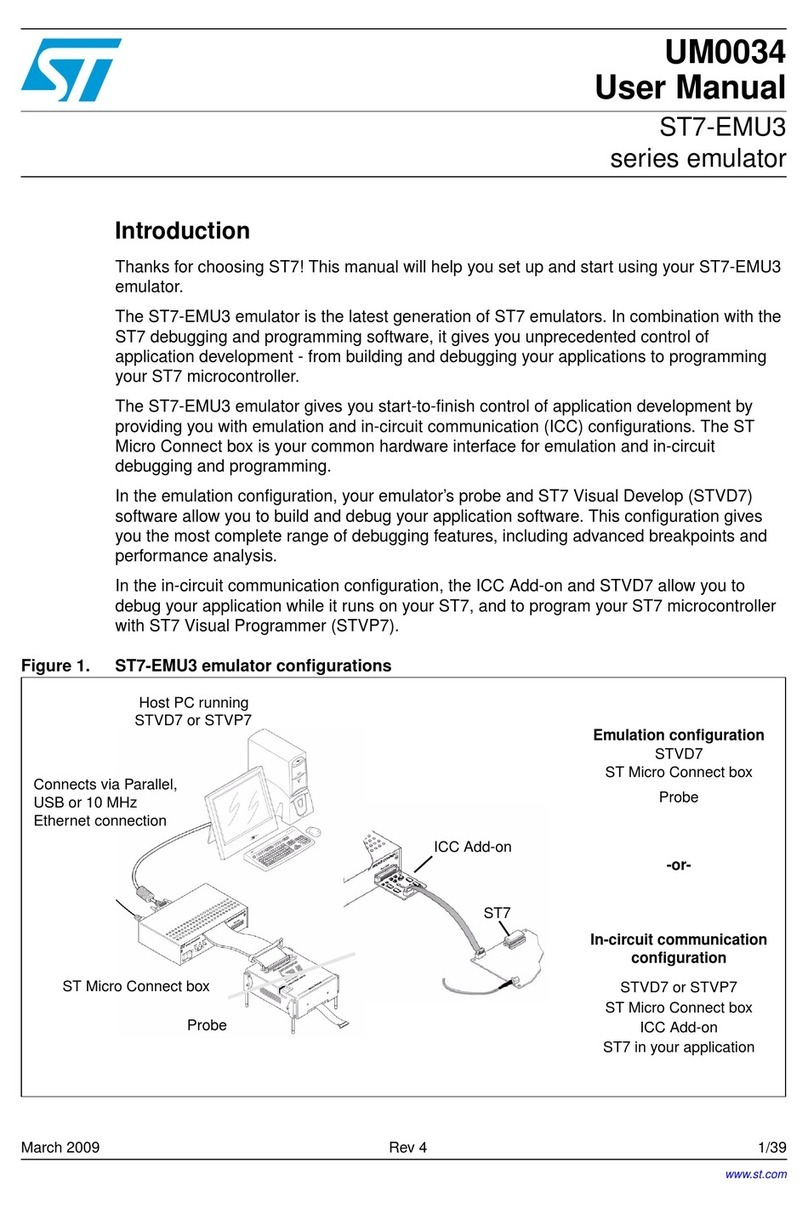
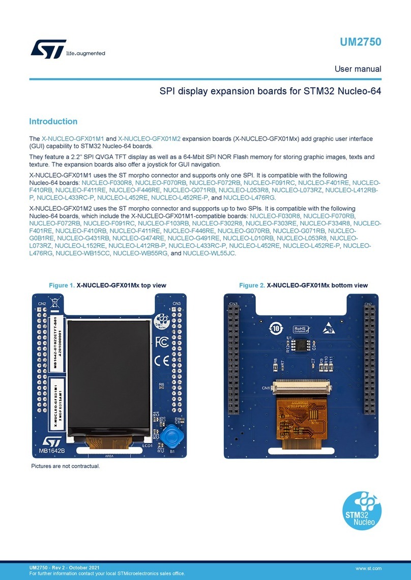
ST X-NUCLEO-IHM07M1 User manual

September 2015
DocID028304 Rev 1
1/28
www.st.com
UM1943
User manual
Getting started with the X-NUCLEO-IHM07M1 motor driver
expansion board based on the L6230 for STM32 Nucleo
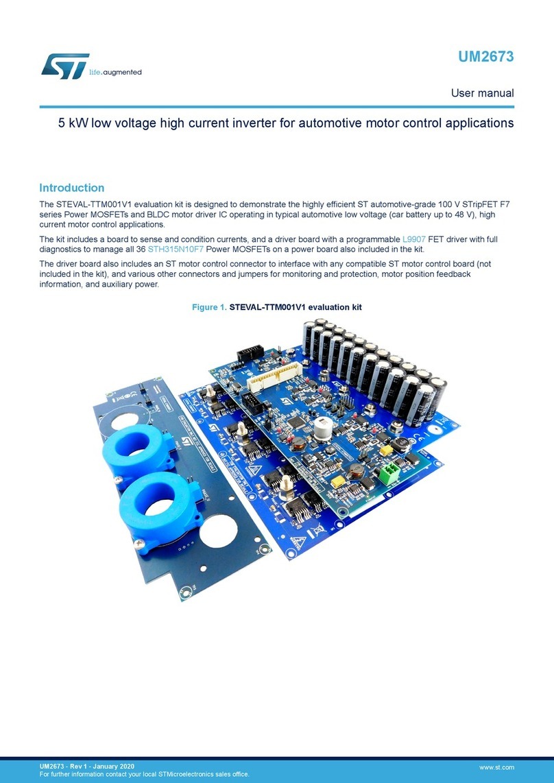
Introduction
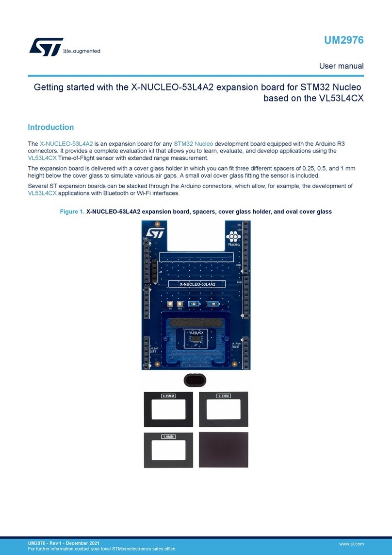
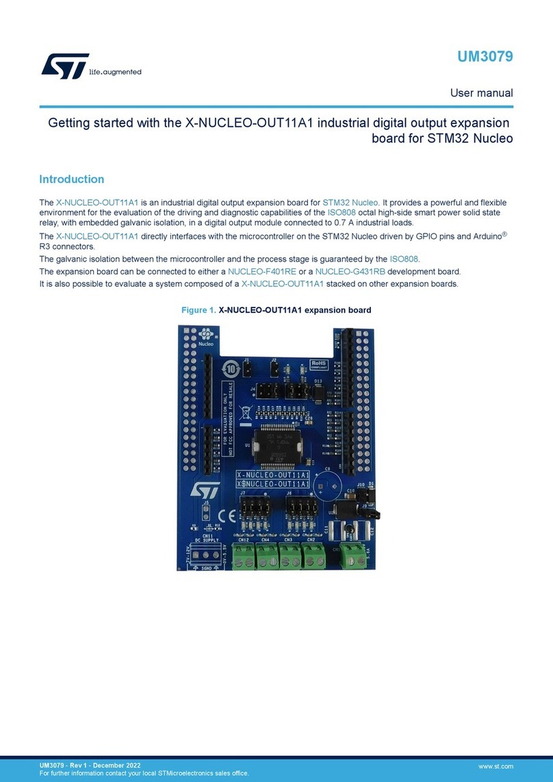
The X-NUCLEO-IHM07M1 is a three-phase brushless DC motor driver expansion board based on the
L6230 for STM32 Nucleo. It provides an affordable and easy-to-use solution for driving three-phase
brushless DC motors in your STM32 Nucleo project. The X-NUCLEO-IHM07M1 is compatible with the
ST morpho connector and supports the addition of other boards which can be stacked onto a single
STM32 Nucleo board. The user can also mount the Arduino UNO R3 connector. The X-NUCLEO-
IHM07M1 is fully configurable and ready to support different closed loop control based on sensor or
sensorless mode control, and it is compatible with three shunt or single shunt current sense measuring.
The driver used on this STM32 Nucleo expansion board is the L6230, a DMOS fully-integrated driver for
three-phase brushless PMSM motors, assembled in a PowerSO36 package, with overcurrent and
thermal protection. This user manual describes the procedure to configure the X-NUCLEO-IHM07M1
expansion board to operate with an STM32 Nucleo board.
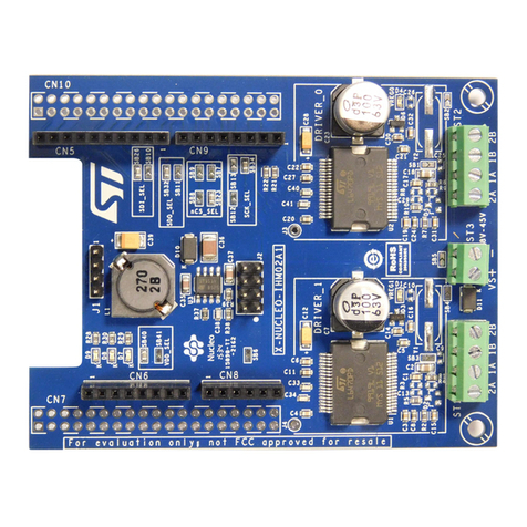
Figure 1: X-NUCLEO-IHM07M1 three-phase brushless DC motor driver expansion board based on L6230 for
STM32 Nucleo

Contents
UM1943
2/28
DocID028304 Rev 1
Contents
1System introduction.........................................................................3
1.1 Main characteristics ..........................................................................3
1.2 Target applications............................................................................3
2Getting started..................................................................................4
2.1 System architecture ..........................................................................4
2.2 Building the system...........................................................................4
2.2.1 Hardware settings............................................................................... 5
3Board schematic.............................................................................10
4Circuit description..........................................................................18
4.1 Power section –L6230 driver with integrated three-phase bridge...18
4.2 Power section –Overcurrent detection (OCP) and current sensing
measurement...............................................................................................19
4.3 Analog section –Hall/Encoder motor speed sensor........................21
4.4 Analog section –BEMF detection circuit.........................................21
4.5 Analog section –Bus voltage and temperature sensing circuit.......21
5BOM (bill of material) .....................................................................23
6Revision history..............................................................................27

UM1943
System introduction
DocID028304 Rev 1
3/28
1 System introduction
1.1 Main characteristics
The list below provides the board specification data and the main parameters for the X-
NUCLEO-IHM07M1 expansion board:
Three-phase driver board for BLDC/PMSM motors
Nominal operating voltage range from 8 V to 48 V DC
2.8 A output peak current (1.4 ARMS)
Operating frequency up to 100 kHz
Non dissipative overcurrent detection and protection
Cross-conduction protection
Thermal measuring and overheating protection
Full compatibility with ST Six Step or ST FOC control algorithms
Full support for sensor and sensorless mode
3-shunt and 1-shunt configurable jumpers for motor current sensing
Hall/Encoder motor sensor connector and circuit
Debug connector for DAC, GPIOs, etc.
Potentiometer available for speed regulation
Fully populated board conception with test points
User LED
Compatible with STM32 Nucleo boards
Equipped with ST morpho connectors
RoHS compliant
PCB type and size:
PCB material: FR-4
4-layer layout
Copper thickness: 70 μm (external layer), 35 μm (internal layer)
Total dimensions of the board: 70 mm x 66 mm
1.2 Target applications
Low voltage PMSM motor driver
Low power fans
Power tools
Industrial drives

Getting started
UM1943
4/28
DocID028304 Rev 1
2 Getting started
2.1 System architecture
A generic motor control system can be schematized in three main blocks (see Figure 2:
"Overall system architecture"):
Control block - its main task is to accept user commands and drive a motor. The X-
NUCLEO-IHM07M1 is based on the STM32 Nucleo board, which provides all digital
signals to properly implement motor driver control.
Power block - it is based on three-phase inverter topology. The core of the power
block is the L6230 driver, which contains all the necessary active power and analog
components to perform low voltage PMSM motor control.
Motor - the X-NUCLEO-IHM07M1 is able to properly drive a low voltage BLDC/PMSM
motor.
Figure 2: Overall system architecture
2.2 Building the system
The X-NUCLEO-IHM07M1 expansion board is a complete hardware development platform
(Power block) for the STM32 Nucleo board, for evaluating a motor control solution for a
single BLDC/PMSM motor. For normal board operation, it must be connected to an STM32
Nucleo board (Control block) through the ST morpho connector, as shown in the image
below.

UM1943
Getting started
DocID028304 Rev 1
5/28
Figure 3: X-NUCLEO-IHM07M1 plugged on STM32 Nucleo
The interconnection between the STM32 Nucleo and the X-NUCLEO-IHM07M1 has been
designed for full-compatibility with many STM32 Nucleo boards and no solder bridge
modification is required. When stacked, the system is ready to operate with the connection
of a BLDC/PMSM motor. For proper use, please respect the hardware and software
settings. For the software details, refer to the X-CUBE-SPN7 software expansion
documents available on www.st.com.
2.2.1 Hardware settings
Table 1: Jumper settings
Jumper
Permitted configurations
Default
condition
JP1
Selection for pull-up insertion (BIAS) in current sensing circuit
OPEN
JP2
Selection for op amp gain modification in current sensing circuit
OPEN
JP3
Selection for pull-up enabling in Hall/Encoder detection circuit
CLOSED
J9
Selection to supply the STM32 Nucleo board through the X-NUCLEO-
IHM07M(1)
OPEN
J5
Selection for single/three shunt configuration. Set to single shunt by
default
2-3 CLOSED
J6
Selection for single/three shunt configuration. Set to single shunt by
default
2-3 CLOSED
J7
Debug connector for DAC. Available for probe connection
OPEN
Notes:
(1)It is recommended to REMOVE jumper J9 before power-on on J1

Getting started
UM1943
6/28
DocID028304 Rev 1
With J9 closed, it is mandatory not to exceed 12 V DC on the J1 connector to avoid
damage to the STM32 Nucleo board.
Jumper JP5 (STM32 Nucleo board) MUST be connected between pin 2 and 3 to enable
the STM32 Nucleo external power supply.
Table 2: Screw terminal table
Screw terminal
Function
J1
Motor power supply input (8 V- 48 V DC)
J2
3-phase motor connector
Figure 4: X-NUCLEO-IHM07M1 –top layer with silk-screen
The X-NUCLEO-IHM07M1 expansion board is equipped with the ST morpho connector,
male pin headers (CN7 and CN10) accessible on both sides of the board. They can be
used to connect the power board to the STM32 Nucleo board. All signals and power pins of
the MCU are available on the ST morpho connector. For further details, please refer to user
manual UM1724 (5.12 STMicroelectronics morpho connector) available on www.st.com.
Table 3: ST morpho connector table
Connector
Pin
Default
Signal
Solder bridge
CN7
1
PC10
Enable_CH1-L6230
R58
2
PC11
Enable_CH2-L6230
R67
3
PC12
Enable_CH3-L6230
R72
4
PD2
5
VDD
6
E5V
7
BOOT0
8
GND
9
NC/PF6

UM1943
Getting started
DocID028304 Rev 1
7/28
Connector
Pin
Default
Signal
Solder bridge
10
NC
11
NC/PF7
12
IOREF
13
PA13
14
RESET
15
PA14
16
+3V3
17
PA15
Encoder A/Hall H1
R79
18
+5V
Encoder/Hall PS voltage
19
GND
20
GND
21
PB7
22
GND
23
PC13
Blue button
24
VIN
J9
25
PC14
26
NC
27
PC15
28
PA0
Curr_fdbk_PhA
R47
29
PH0/PF0/PD0
30
PA1
VBUS_sensing
R51
31
PH1/PF1/PD1
32
PA4
DAC_Ch
R76 N.M.
33
VLCD/VBAT
34
PB0
BEMF2_sensing
R60
35
PC2
Temperature feedback
R54
36
PC1 or PB9(1)
Curr_fdbk_PhB
R48
37
PC3
BEMF1_sensing
R59
38
PC0 or PB8(2)
Curr_fdbk_PhC
R50
CN10
1
PC9
2
PC8
3
PB8
4
PC6
5
PB9
6
PC5
7
AVDD
8
U5V(3)

Getting started
UM1943
8/28
DocID028304 Rev 1
Connector
Pin
Default
Signal
Solder bridge
9
GND
10
NC
11
PA5(4)
GPIO/DAC/PWM
R80
12
PA12
CPOUT
R52
13
PA6(5)
DIAG/ENABLE/BKIN1
R53
14
PA11
DIAG/ENABLE/BKIN2
R46
15
PA7(6)
BEMF3_sensing
R63
16
PB12
17
PB6
18
PB11/NC
19
PC7
20
GND
21
PA9
VH_PWM
R64
22
PB2
LED RED
R83
23
PA8
UH_PWM
R56
24
PB1
POTENTIOMETER
R78
25
PB10
Encoder Z/Hall H3
R84
26
PB15(7)
BEMF3_sensing
R66
27
PB4
CURRENT REF
R77
28
PB14(8)
DIAG/ENABLE/BKIN1
R49
29
PB5
GPIO/DAC/PWM
R85
30
PB13(9)
GPIO/DAC/PWM
R82
31
PB3
Encoder B/Hall H2
R81
32
AGND
33
PA10
WH_PWM
R70
34
PC4
35
PA2
36
NC/PF5
37
PA3
38
NC/PF4
Notes:
(1)Please refer to Table 9: Solder bridges in user manual UM1724 for further details
(2)Please refer to Table 9: Solder bridges in user manual UM1724 for further details
(3)U5V is 5 V power from ST-LINK/V2-1 USB connector and it rises before +5 V
(4)For STM32F302-Nucleo only:
- pin PA5 is on CN10/pin 30 and PB13 is on CN10/pin 11
- pin PA6 is on CN10/pin 28 and PB14 is on CN10/pin 13
- pin PA7 is on CN10/pin 26 and PB15 is on CN10/pin 13

UM1943
Getting started
DocID028304 Rev 1
9/28
(5)For STM32F302-Nucleo only:
- pin PA5 is on CN10/pin 30 and PB13 is on CN10/pin 11
- pin PA6 is on CN10/pin 28 and PB14 is on CN10/pin 13
- pin PA7 is on CN10/pin 26 and PB15 is on CN10/pin 13
(6)For STM32F302-Nucleo only:
- pin PA5 is on CN10/pin 30 and PB13 is on CN10/pin 11
- pin PA6 is on CN10/pin 28 and PB14 is on CN10/pin 13
- pin PA7 is on CN10/pin 26 and PB15 is on CN10/pin 13
(7)For STM32F302-Nucleo only:
- pin PA5 is on CN10/pin 30 and PB13 is on CN10/pin 11
- pin PA6 is on CN10/pin 28 and PB14 is on CN10/pin 13
- pin PA7 is on CN10/pin 26 and PB15 is on CN10/pin 13
(8)For STM32F302-Nucleo only:
- pin PA5 is on CN10/pin 30 and PB13 is on CN10/pin 11
- pin PA6 is on CN10/pin 28 and PB14 is on CN10/pin 13
- pin PA7 is on CN10/pin 26 and PB15 is on CN10/pin 13
(9)For STM32F302-Nucleo only:
- pin PA5 is on CN10/pin 30 and PB13 is on CN10/pin 11
- pin PA6 is on CN10/pin 28 and PB14 is on CN10/pin 13
- pin PA7 is on CN10/pin 26 and PB15 is on CN10/pin 13

Board schematic
UM1943
10/28
DocID028304 Rev 1
3 Board schematic
Figure 5: X-NUCLEO-IHM07M1 schematic (1 of 8)
Vshunt_3_GND
Vshunt_2_GND
Vshunt_1_GND
Externaloperational-amplifier
Overall AV=1.53
3V3
3V3
3V3
3V3
3V3
3V3
3V3
Vshunt_1
Curr_fdbk1
Curr_fdbk2
CP+
Vshunt_2
Curr_fdbk3
Vshunt_3
C8
N.M. 100pF/6.3V
JP1
FOC
R11
2.2k
C4
N.M. 100pF/6.3V
R13
680
C1
100nF10V
R9
2.2k
-
+U10C
TSV994IPT
10
98
4
11
-
+U10D
TSV994IPT
12
13 14
4
11
R10 2.2k
C3
680pF 10V
0 3R
R15
2.2k
R1
2.2k
C7
680pF 10V
R5 2.2k
R4
2.2k
R14
0
R8
0
R2680
R12
2.2k
C5
680pF 10V
-
+U10B
TSV994IPT
5
67
4
11
-
+U10A
TSV994IPT
3
21
4
11
R7
680
R16
2.2k
R6
2.2k
C6
N.M. 100pF/6.3V
JP2 FOC
C2
4.7uF 10V
GSPG03092015DI0955

UM1943
Board schematic
DocID028304 Rev 1
11/28
Figure 6: X-NUCLEO-IHM07M1 schematic (2 of 8)
HALL/ENCODER SENSOR
5V
GND
A+/H1
B+/H2
Z+/H3
3V33V3
5V
A+/H1
B+/H2
Z+/H3
R30
1k8
JP3
JUMPER
C20
10pF10V
R32
1k8 R34
4K7N.M.
R31
1k8
R33
4K7N.M.
R29
10k
J3
Stripline m. 1x5
1
2
3
4
5C22
10pF10V
R28
10k
R27
10k
D4
BAT30KFILM
D3
BAT30KFILM
D2
BAT30KFILM
C19
100n
R35
4K7N.M.
J4
RING
1
C21
10pF10V
SPEED REGULATION
SPEED
3V3
SPEED
R42
100K
SHUNT RESISTOR
Vshunt_1_GND
Vshunt_2_GND Vshunt_3_GND
Vshunt_1 Vshunt_2 Vshunt_3
R45
0.331W
R44
0.331W
R43
0.331W
RS model 742-8420
Placed nearthe L6230 driver
3V3
Temperature feedba ck
R19
NTC 10K
2
1R20
4K7
C10 10nF10V
VBUS SENSOR
VBUS_SENS
VIN+
VBUS
C14
4.7nF/10V
R18
9.31K1%
R17
169K1%
GSPG03092015DI1000

Board schematic
UM1943
12/28
DocID028304 Rev 1
Figure 7: X-NUCLEO-IHM07M1 schematic (3 of 8)
L6230 DMOS driver for three-phase brushless DC motor
POWER CONNECTOR
OUT1
OUT2
OUT3
SENS1
SENS2
SENS3
CPOUT
IN1
EN1
EN3
IN3
EN2
IN2
CP+
CP-
VIN+
3V3
3V3
Vshunt_2
EN3 IN3
EN2 IN2
DIAG/EN
CURRENTREF
CPOUT
CP+
IN1
EN1
R21
33K
J16
RING
1
R25
39k
R23
10K
roto
M2
J
1
2
3
C13
100nF/100V
C17
1nF/6.3V
D1
SMBD 7000
12
3
C18
10n-N.M.
C15
100uF, 63V
C12
10n100V
U11
L6230PD
IN1
9CPOUT
24
VSA
4
N.C. 3
N.C. 2
GND 1
OUT3
32
N.C. 31
VBOOT
30
EN3 29
CP-
28
VCP
7
CP+
13
N.C. 14
OUT1
15
N.C. 16
N.C. 17
GND 18
GND 19
N.C. 20
N.C. 21
EN1
10
SENS1 12
N.C. 23
N.C. 6
IN2 26
SENS2 8
SENS3 25
EN2 27
IN3 11
OUT2
5
DIAG/EN 22
VSB
33
N.C. 34
N.C. 35
GND 36
EP 37
C16
100n,6.3V
R22
10K
C9
220nF, 16V
C11
100nF/100V
R26
39k
D12
SMBJ48A-TR
R24
39k
J1
CON2
1
2
GSPG03092015DI1005

UM1943
Board schematic
DocID028304 Rev 1
13/28
Figure 8: X-NUCLEO-IHM07M1 schematic (4 of 8)
3Sh
1Sh
3Sh
1Sh
BEMFDETECTION
- SIXSTEP
SINGLE/THREE SHUNT CONFIGURATION
OUT1 OUT2 OUT3
GPIO_BEMF GPIO_BEMF GPIO_BEMF
BEMF1 BEMF3
3V33V33V3
3V3
GPIO_BEMF
BEMF1 BEMF2
GPIO_BEMF GPIO_BEMF
BEMF3
Vshunt_3
SENS3
Vshunt_2
Vshunt_1
SENS1
Vshunt_2
R39
10k
J6
CON3 1
2
3
R36
2.2k
D10
BAT30KFILM
D6
BAT30KFILM
R41
10k
J5
CON3 1
2
3
D9
BAT30KFILM
D5
BAT30KFILM D8
BAT30KFILM
R38
2.2k
C23
0.1uF/6.3V
R40
10k
D7
BAT30KFILM
R37
2.2k
GSPG03092015DI1010

Board schematic
UM1943
14/28
DocID028304 Rev 1
Figure 9: X-NUCLEO-IHM07M1 schematic (5 of 8)
F302
PWM
PA8-UH
PA6-BKIN
PA9-VH
PA10-WH
PC12
PC11
PC10
PA11
DIAG/EN
IN1
EN1
IN2
EN2
IN3
EN3
C10_14
C10_28
C10_13
C10_23
C7_1
C10_21
C7_2
C10_33
C7_3
R58
0
R46
0
R64
0
R70
0
R67
0
R53
0
R72
0
R56
0
R49
0
HALL/ENCODERSENSOR
PA15 - Enc. A/H1
PB3 - Enc. B/H2
PB10 - Enc. Z/H3
C7_17
C10_31
C10_25 Z+/H3
A+/H1
B+/H2
R81 0
R79 0
R84 0
DAC/REF
F302 PA5/PB13
PA4- DAC
PB4-PWM
PA5 - DAC
PB5-DAC PWM
CURRENT REF
C7_32
C10_27
C10_11
C10_30
C10_29 0 28R
J8
RING 1
0 08R
J7
Stripline m. 1x3
1
2
3
0 77R
R76
0-N.M.
0 58R
Currents
F302
EmbPGA
PA0 - PhA
PC1 - PhB
PC0 - PhC
PA1 - BUSV
PC2 - Temp. Sens.
PA1 - EmbPGA
PA7 - EmbPGA
PB0 - EmbPGA
3V3
C7_28
C7_38
C7_35
Curr_fdbk1
Curr_fdbk2
Curr_fdbk3
VBUS
Temperature feedback
C7_30
C10_15
C7_34
Vshunt_1
Vshunt_2
C10_26
Vshunt_3
C7_36
C7_30
0 74R
R73 0
0 45R
R69
N.M.13K 1%
R65 0
R74
N.N. 4.99K
R68
N.N. 4.99K
R61
N.N. 4.99K
R71 0-N.M.
0 15R
0 84R
005R
0 75R
R62 N.M.13K 1%
R75
N.M.13K 1%
GSPG03092015DI1015

UM1943
Board schematic
DocID028304 Rev 1
15/28
Figure 10: X-NUCLEO-IHM07M1 schematic (6 of 8)
STM32 NUCLEO PART USED
PC13 - START/STOP (B1 BUTTON)
RESET - MCU RST (B2 BUTTON)
VIN
VIN+
C7_24
J9
JUMPER VIN 3A 12
Open by default J27 on:
1) 12 VMAX on J26
2) JP5 (Nucleo pin 2, 3)
2) JP1 (Nucleo) removed
USER
PB1
PB2
C10_24
C10_22
SPEED
D11
RED
087R
R83
510
BEMF six STEP
F302
PC9 - GPIO
PC3 - ADC
PB0 - ADC
PA7 - ADC
PA12- TIM1 ETR
C10_12
C10_1
C7_37
C7_34
C10_15
C10_26
CPOUT
GPIO_BEMF
BEMF1
BEMF2
BEMF3
025R
0 66R
0 95R
0 36R
0 06R
0 55R
GSPG03092015DI1020

Board schematic
UM1943
16/28
DocID028304 Rev 1
Figure 11: X-NUCLEO-IHM07M1 schematic (7 of 8)
ARDUINO/STMORPHO CONNECTOR
C7_1
C7_3
C7_5
C7_7
C7_13
C7_15
C7_17
C7_19
C7_21
C7_23
C7_25
C7_27
C7_29
C7_31
C7_33
C7_35
C7_37
C7_14C6_3
C7_16
C7_18C6_5
C7_20
C7_22
C7_24C6_8
C7_28C8_1
C7_38C8_6
C7_36C8_5
C7_34C8_4
C7_30C8_2
C7_32C8_3
C7_2
C7_4
E5V C7_6
C7_8 C10_3
C5_10
C10_7
C5_8 C10_9
C5_7 C10_11
C5_6 C10_13
C5_5 C10_15
C5_4 C10_17
C5_3 C10_19
C5_2 C10_21
C5_1
C10_5
C5_9
C10_35
C9_2
C10_29
C9_5 C10_31
C9_4
C10_25
C9_7
C10_33
C9_3
C10_27
C9_6
C10_23
C9_8
C10_37
C9_1
C10_1 C10_2
C10_4
C10_6
C10_8
C10_10
C10_12
C10_14
C10_16
C10_18
C10_20
C10_22
C10_24
C10_26
C10_28
C10_30
C10_32
C10_34
C10_36
C10_38
C7_9
C7_11 C7_12 C6_1 N.C.
C6_2 +3V3
C6_6
N.C. C7_10
C6_7
C7_26
C6_4
C7_18
3V3
5V
CN6
1
2
3
4
5
6
7
8
CN5
1
2
3
4
5
6
7
8
9
10
CN10
12
34
56
78
910
11 12
13 14
15 16
17 18
19 20
21 22
23 24
25 26
27 28
29 30
31 32
33 34
35 36
37 38
CN7
12
34
56
78
910
11 12
13 14
15 16
17 18
19 20
21 22
23 24
25 26
27 28
29 30
31 32
33 34
35 36
37 38 CN8
1
2
3
4
5
6
CN91
2
3
4
5
6
7
8
GSPG03092015DI1410

UM1943
Board schematic
DocID028304 Rev 1
17/28
Figure 12: X-NUCLEO-IHM07M1 schematic (8 of 8)
L6230 DMOS driver for three-phase brushless DC motor
POWER CONNECTOR
OUT1
OUT2
OUT3
SENS1
SENS2
SENS3
CPOUT
IN1
EN1
EN3
IN3
EN2
IN2
CP+
CP-
VIN+
3V3
3V3
Vshunt_2
EN3 IN3
EN2 IN2
DIAG/EN
CURRENTREF
CPOUT
CP+
IN1
EN1
R21
33K
J16
RING
1
R25
39k
R23
10K
rotoM 2J
1
2
3
C13
100nF/100V
C17
1nF/6.3V
D1
SMBD 7000
12
3
C18
10n-N.M.
C15
100uF, 63V
C12
10n100V
U11
L6230PD
IN1
9CPOUT
24
VSA
4
N.C. 3
N.C. 2
GND 1
OUT3
32
N.C. 31
VBOOT
30
EN3 29
CP-
28
VCP
7
CP+
13
N.C. 14
OUT1
15
N.C. 16
N.C. 17
GND 18
GND 19
N.C. 20
N.C. 21
EN1
10
SENS1 12
N.C. 23
N.C. 6
IN2 26
SENS2 8
SENS3 25
EN2 27
IN3 11
OUT2
5
DIAG/EN 22
VSB
33
N.C. 34
N.C. 35
GND 36
EP 37
C16
100n,6.3V
R22
10K
C9
220nF, 16V
C11
100nF/100V
R26
39k
D12
SMBJ48A-TR
R24
39k
J1
CON2
1
2
GSPG03092015DI1415

Circuit description
UM1943
18/28
DocID028304 Rev 1
4 Circuit description
4.1 Power section –L6230 driver with integrated three-phase
bridge
The main section is based on the L6230. It is a DMOS fully-configurable driver for three-
phase brushless BLDC/PMSM motors. The supply voltage is provided through an external
connector (J1) and with (J9) jumper settings, it is possible to choose if the digital section
(STM32 Nucleo board) must be supplied by USB or by the expansion board. For these
settings, please refer to Table 1: "Jumper settings".
Figure 13: X-NUCLEO-IHM07M1 –power section
The L6230 integrates a three-phase bridge which consists of six power MOSFETs. Using
the N-channel power MOSFET for the upper transistors in the bridge requires a gate drive
voltage above the power supply voltage. The bootstrapped supply (VBOOT) is obtained
through an internal oscillator and a few external components to implement a charge pump
circuit as shown in the diagram that follows.

UM1943
Circuit description
DocID028304 Rev 1
19/28
Figure 14: X-NUCLEO-IHM07M1 –charge pump circuit
4.2 Power section –Overcurrent detection (OCP) and current
sensing measurement
The L6230 driver implements overcurrent protection with an internal detection circuit that
does not require an external resistor. The current is compared with an embedded current
reference and the output generates a fault condition to the DIAG pin that goes to ground.
U11
L6230PD
IN1
9CPOUT
24
VSA
4
N.C.3
N.C.2
GND 1
OUT3
32
N.C.31
VBOOT
30
EN3 29
CP-
28
VCP
7
CP+
13
N.C.14
OUT1
15
N.C.16
N.C.17
GND 18
GND 19
N.C.20
N.C.21
EN1
10
SENS1 12
N.C.23
N.C.6
IN226
SENS2 8
SENS3 25
EN2 27
IN311
OUT2
5
DIAG/EN 22
VSB
33
N.C.34
N.C.35
GND 36
EP 37
D12
SMBJ48A-TR
C12
10n 100V
C9
220nF, 16V
VIN+
C13
100nF/100V
C15
100uF, 63V
J16
RING
1
CP-
C11
100nF/100V
CPOUT
R21
33K
J1
CON2
1
2
CP+
CURRENT REF CP+
D1
SMBD 7000
12
3
GSPG14092015DI1535

Circuit description
UM1943
20/28
DocID028304 Rev 1
This pin, connected to the STM32 Nucleo board (BKIN Timer function), detects this
condition and immediately disables the driving signals.The current sensing input is
connected to the sensing resistors Rsense (refer to the diagram below) and it is possible to
choose between three-shunt or single-shunt configuration through the jumpers (J5, J6). For
this setting please refer to Table 1: "Jumper settings".
Figure 15: X-NUCLEO-IHM07M1 –current sensing circuit
U11
L6230PD
IN1
9CPOUT
24
VSA
4
N.C. 3
N.C. 2
GND 1
OUT3
32
N.C. 31
VBOOT
30
EN3 29
CP-
28
VCP
7
CP+
13
N.C. 14
OUT1
15
N.C. 16
N.C. 17
GND 18
GND 19
N.C. 20
N.C. 21
EN1
10
SENS1 12
N.C. 23
N.C. 6
IN226
SENS2 8
SENS3 25
EN2 27
IN311
OUT2
5
DIAG/EN 22
VSB
33
N.C. 34
N.C. 35
GND 36
EP 37
OUT1
OUT2
J2Motor
1
2
3
OUT3
J5
CON31
2
3
J6
CON31
2
3
R43
0.33 1W R44
0.33 1W R45
0.33 1W
SENS1
SENS2
3V3
SENS3
IN3
EN3
IN2
EN2
R25
39k R26
39k C17
1nF/6.3V
R22
10K
Vshunt_2
EN3 IN3
EN2 IN2
DIAG/EN
Vshunt_3
SENS3
Vshunt_2
Vshunt_1
SENS1
Vshunt_2
Vshunt_1 Vshunt_2 Vshunt_3
GSPG14092015DI1540
Table of contents
Other ST Computer Hardware manuals

ST
ST STM32H573I-DK User manual

ST
ST STM32F411 User manual

ST
ST X-NUCLEO-LED12A1 User manual

ST
ST STM32F4 Series Owner's manual

ST
ST X-NUCLEO-OUT11A1 User manual
ST
ST STM32 ODE User manual

ST
ST X-NUCLEO-BNRG2A1 User manual

ST
ST STM32F038 6 Series User manual

ST
ST X-NUCLEO-OUT02A1 User manual

ST
ST AEK-COM-ISOSPI1 User manual

ST
ST 32L152CDISCOVERY User manual

ST
ST STEVAL-CCH002V2 User manual

ST
ST B-WB1M-WPAN1 User manual

ST
ST B-U585I-IOT02A User manual

ST
ST STEVAL-IFP044V1 User manual

ST
ST X-NUCLEO-OUT02A1 User manual

ST
ST ST32M103 Series User manual

ST
ST M41ST85W User manual

ST
ST X-NUCLEO-OUT06A1 User manual

ST
ST X-NUCLEO-OUT13A1 User manual