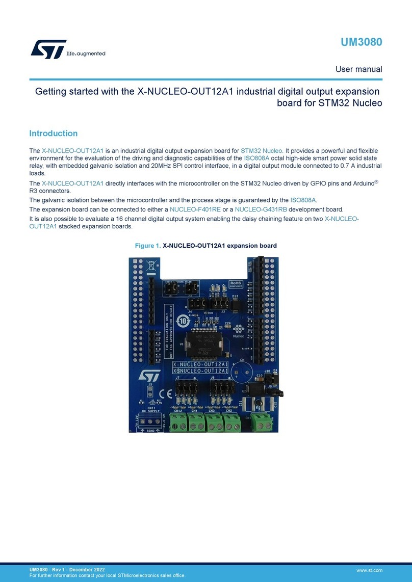
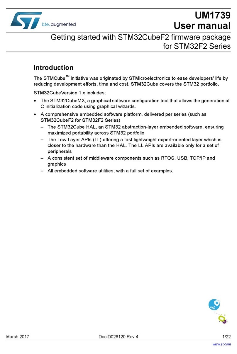
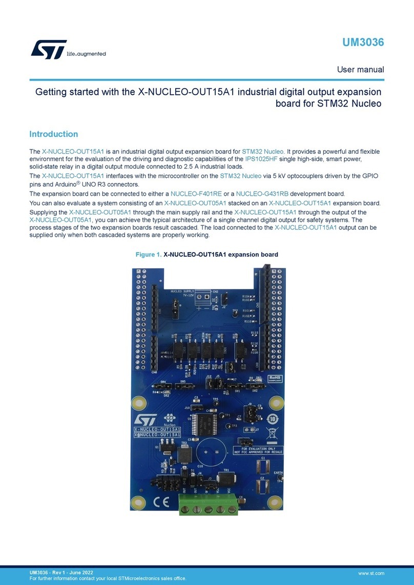
ST STM32F3DISCOVERY User manual

September 2012 Doc ID 023594 Rev 2 1/36
UM1570
User manual
STM32F3DISCOVERY
Discovery kit for STM32F303xx microcontrollers
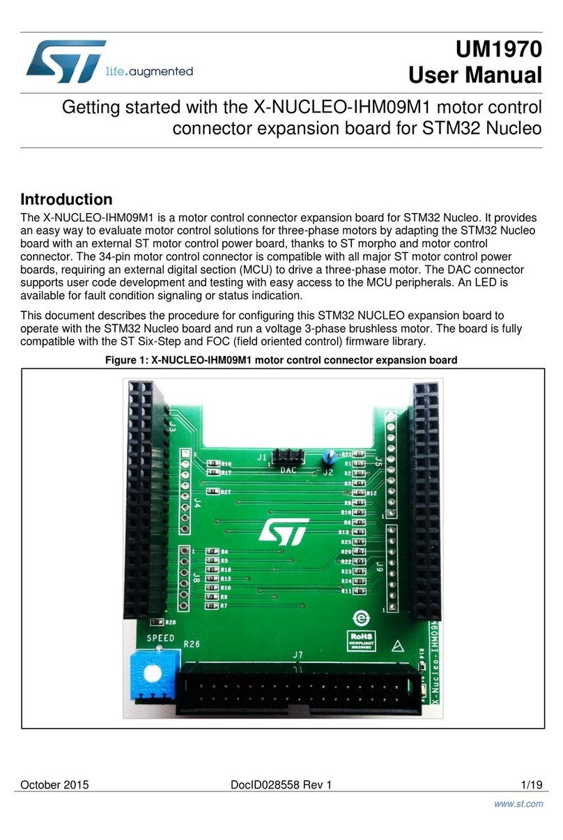
Introduction
The STM32F3DISCOVERY is designed to help you explore the features of the STM32 F3
32-bit ARM® Cortex™-M4 mixed-signal MCU, and develop your applications. It is based on
an STM32F303VCT6 and includes an ST-LINK/V2 embedded debug tool interface,
Gyroscope ST MEMS, E-compass with accelerometer ST MEMS, LEDs, pushbuttons and a
USB mini-B connector.
Figure 1. STM32F3DISCOVERY
Table 1. Applicable tools
Type Part number
Evaluation tools STM32F3DISCOVERY
www.st.com

Contents UM1570
2/36 Doc ID 023594 Rev 2
Contents
1 Conventions . . . . . . . . . . . . . . . . . . . . . . . . . . . . . . . . . . . . . . . . . . . . . . . . 5
2 Quick start . . . . . . . . . . . . . . . . . . . . . . . . . . . . . . . . . . . . . . . . . . . . . . . . . 6
2.1 Getting started . . . . . . . . . . . . . . . . . . . . . . . . . . . . . . . . . . . . . . . . . . . . . . 6
2.2 System requirements . . . . . . . . . . . . . . . . . . . . . . . . . . . . . . . . . . . . . . . . . 6
2.3 Development toolchain supporting the STM32F3DISCOVERY . . . . . . . . . 6
2.4 Order code . . . . . . . . . . . . . . . . . . . . . . . . . . . . . . . . . . . . . . . . . . . . . . . . . 6
3 Features . . . . . . . . . . . . . . . . . . . . . . . . . . . . . . . . . . . . . . . . . . . . . . . . . . . 7
4 Hardware and layout . . . . . . . . . . . . . . . . . . . . . . . . . . . . . . . . . . . . . . . . . 8
4.1 STM32F303VCT6 microcontroller . . . . . . . . . . . . . . . . . . . . . . . . . . . . . . 11
4.2 Embedded ST-LINK/V2 . . . . . . . . . . . . . . . . . . . . . . . . . . . . . . . . . . . . . . 14
4.2.1 Using ST-LINK/V2 to program/debug the STM32F303VCT6 on board . 14
4.2.2 Using ST-LINK/V2 to program/debug an external STM32 application . . 15
4.3 Power supply and power selection . . . . . . . . . . . . . . . . . . . . . . . . . . . . . . 17
4.4 LEDs . . . . . . . . . . . . . . . . . . . . . . . . . . . . . . . . . . . . . . . . . . . . . . . . . . . . 17
4.5 Pushbuttons . . . . . . . . . . . . . . . . . . . . . . . . . . . . . . . . . . . . . . . . . . . . . . . 17
4.6 USB device supported . . . . . . . . . . . . . . . . . . . . . . . . . . . . . . . . . . . . . . . 18
4.7 E-compass/accelerometer MEMS (ST MEMS LSM303DLHC) . . . . . . . . 18
4.8 Gyroscope MEMS (ST MEMS L3GD20) . . . . . . . . . . . . . . . . . . . . . . . . . 18
4.9 JP3 (Idd) . . . . . . . . . . . . . . . . . . . . . . . . . . . . . . . . . . . . . . . . . . . . . . . . . . 18
4.10 OSC clock . . . . . . . . . . . . . . . . . . . . . . . . . . . . . . . . . . . . . . . . . . . . . . . . 19
4.10.1 OSC clock supply . . . . . . . . . . . . . . . . . . . . . . . . . . . . . . . . . . . . . . . . . 19
4.10.2 OSC 32 kHz clock supply . . . . . . . . . . . . . . . . . . . . . . . . . . . . . . . . . . . 19
4.11 Solder bridges . . . . . . . . . . . . . . . . . . . . . . . . . . . . . . . . . . . . . . . . . . . . . 20
4.12 Extension connectors . . . . . . . . . . . . . . . . . . . . . . . . . . . . . . . . . . . . . . . . 21
5 Mechanical drawing . . . . . . . . . . . . . . . . . . . . . . . . . . . . . . . . . . . . . . . . 30
6 STM32F3DISCOVERY electrical schematics . . . . . . . . . . . . . . . . . . . . . 31
7 Revision history . . . . . . . . . . . . . . . . . . . . . . . . . . . . . . . . . . . . . . . . . . . 35

UM1570 List of figures
Doc ID 023594 Rev 2 3/36
List of figures
Figure 1. STM32F3DISCOVERY. . . . . . . . . . . . . . . . . . . . . . . . . . . . . . . . . . . . . . . . . . . . . . . . . . . . . 1
Figure 2. Hardware block diagram . . . . . . . . . . . . . . . . . . . . . . . . . . . . . . . . . . . . . . . . . . . . . . . . . . . . 8
Figure 3. Board layout (top view) . . . . . . . . . . . . . . . . . . . . . . . . . . . . . . . . . . . . . . . . . . . . . . . . . . . . . 9
Figure 4. Board layout (bottom view) . . . . . . . . . . . . . . . . . . . . . . . . . . . . . . . . . . . . . . . . . . . . . . . . . 10
Figure 5. STM32F303VCT6 package . . . . . . . . . . . . . . . . . . . . . . . . . . . . . . . . . . . . . . . . . . . . . . . . 11
Figure 6. STM32F303VCT6 block diagram . . . . . . . . . . . . . . . . . . . . . . . . . . . . . . . . . . . . . . . . . . . . 13
Figure 7. Typical configuration. . . . . . . . . . . . . . . . . . . . . . . . . . . . . . . . . . . . . . . . . . . . . . . . . . . . . . 14
Figure 8. STM32F3DISCOVERY connections image . . . . . . . . . . . . . . . . . . . . . . . . . . . . . . . . . . . . 15
Figure 9. ST-LINK/V2 connections image . . . . . . . . . . . . . . . . . . . . . . . . . . . . . . . . . . . . . . . . . . . . . 16
Figure 10. STM32F3DISCOVERY mechanical drawing . . . . . . . . . . . . . . . . . . . . . . . . . . . . . . . . . . . 30
Figure 11. STM32F3DISCOVERY top level . . . . . . . . . . . . . . . . . . . . . . . . . . . . . . . . . . . . . . . . . . . . 31
Figure 12. ST-LINK/V2 (SWD only) . . . . . . . . . . . . . . . . . . . . . . . . . . . . . . . . . . . . . . . . . . . . . . . . . . . 32
Figure 13. STM32F303VCT6 MCU . . . . . . . . . . . . . . . . . . . . . . . . . . . . . . . . . . . . . . . . . . . . . . . . . . . 33
Figure 14. Peripherals . . . . . . . . . . . . . . . . . . . . . . . . . . . . . . . . . . . . . . . . . . . . . . . . . . . . . . . . . . . . . 34

List of tables UM1570
4/36 Doc ID 023594 Rev 2
List of tables
Table 1. Applicable tools. . . . . . . . . . . . . . . . . . . . . . . . . . . . . . . . . . . . . . . . . . . . . . . . . . . . . . . . . . . 1
Table 2. ON/OFF conventions . . . . . . . . . . . . . . . . . . . . . . . . . . . . . . . . . . . . . . . . . . . . . . . . . . . . . . 5
Table 3. Jumper states . . . . . . . . . . . . . . . . . . . . . . . . . . . . . . . . . . . . . . . . . . . . . . . . . . . . . . . . . . . 14
Table 4. Debug connector CN3 (SWD) . . . . . . . . . . . . . . . . . . . . . . . . . . . . . . . . . . . . . . . . . . . . . . 15
Table 5. Solder bridges. . . . . . . . . . . . . . . . . . . . . . . . . . . . . . . . . . . . . . . . . . . . . . . . . . . . . . . . . . . 20
Table 6. STM32F303VCT6 MCU pin description versus board function . . . . . . . . . . . . . . . . . . . . . 21
Table 7. Document revision history . . . . . . . . . . . . . . . . . . . . . . . . . . . . . . . . . . . . . . . . . . . . . . . . . 35

UM1570 Conventions
Doc ID 023594 Rev 2 5/36
1 Conventions
Tabl e 2 provides the definition of some conventions used in the present document.
Table 2. ON/OFF conventions
Convention Definition
Jumper JP1 ON Jumper fitted
Jumper JP1 OFF Jumper not fitted
Solder bridge SBx ON SBx connections closed by solder
Solder bridge SBx OFF SBx connections left open

Quick start UM1570
6/36 Doc ID 023594 Rev 2
2 Quick start
The STM32F3DISCOVERY is a low-cost and easy-to-use development kit to quickly
evaluate and start development with an STM32 F3 series microcontroller. Before installing
and using the product, please accept the Evaluation Product License Agreement from
www.st.com/stm32f3discovery. For more information on the STM32F3DISCOVERY and for
demonstration software, visit www.st.com/stm32f3discovery.
2.1 Getting started
Follow the sequence below to configure the STM32F3DISCOVERY board and launch the
DISCOVER application:
1. Check the jumper positions on the board, JP3 on, CN4 on (DISCOVERY selected).
2. Connect the STM32F3DISCOVERY board to a PC with a USB cable type A to mini-B
through the USB ST-LINK or USB USER connector to power the board. The red LEDs
LD1 (PWR) and LD2 (COM) light up.
3. The eight LED indicators blink sequentially.
4. Press the USER button to enable the MEMS gyroscope sensor.
5. Observe how the blinking of the LEDs indicates the gyroscope movements.
6. Press the USER button again to enable the MEMS e-compass sensor.
7. Keep the board in a horizontal position. One of the eight LEDs lights up to indicate the
direction of the north.
8. Tilt the board and the eight LEDs blink again
9. To examine or modify the Discover project related to this demo, visit
www.st.com/stm32f3discovery and follow the tutorial. Discover the STM32F303xx MCU
features, download and execute programs proposed in the list of projects.
10. Develop your own application using the available examples.
2.2 System requirements
●Windows PC (XP, Vista, 7)
●USB type A to Mini-B USB cable
2.3 Development toolchain supporting the STM32F3DISCOVERY
●Altium®, TASKING™ VX-toolset
●ARM®, Atollic TrueSTUDIO®
●IAR™, EWARM (IAR Embedded Workbench®)
●Keil™, MDK-ARM™
2.4 Order code
To order the STM32F303xx Discovery kit, use the order code STM32F3DISCOVERY.

UM1570 Features
Doc ID 023594 Rev 2 7/36
3 Features
The STM32F3DISCOVERY offers the following features.
●STM32F303VCT6 microcontroller featuring 256 KB of Flash memory, 48 KB of RAM in
an LQFP100 package.
●On-board ST-LINK/V2 with selection mode switch to use the kit as a standalone
ST-LINK/V2 (with SWD connector for programming and debugging).
●Board power supply: through the USB bus or from an external 3 V or 5 V supply
voltage.
●External application power supply: 3 V and 5 V.
●L3GD20, ST MEMS motion sensor, 3-axis digital output gyroscope.
●LSM303DLHC, ST MEMS system-in-package featuring a 3D digital linear acceleration
sensor and a 3D digital magnetic sensor.
●Te n L E D s :
– LD1 (red) for 3.3 V power-on.
– LD2 (red/green) for USB communication.
– Eight user LEDs, LD3/10 (red), LD4/9 (blue), LD5/8 (orange) and LD6/7 (green).
●Two pushbuttons (user and reset).
●USB USER with Mini-B connector.
●Extension header for LQFP100 I/Os for quick connection to prototyping board and easy
probing.
A large number of free ready-to-run application firmware examples are available at
www.st.com/stm32f3discovery to support quick evaluation and development.

Hardware and layout UM1570
8/36 Doc ID 023594 Rev 2
4 Hardware and layout
The STM32F3DISCOVERY is designed around the STM32F303VCT6 microcontroller in a
100-pin LQFP package.
Figure 2 illustrates the connections between the STM32F303VCT6 and its peripherals
(ST-LINK/V2, pushbutton, LED, USB, Gyroscope ST MEMS, E-compass with accelerometer
ST MEMS, and connectors).
Figure 2 and Figure 3 help you to locate these features on the STM32F3DISCOVERY.
Figure 2. Hardware block diagram
%MBEDDED
34,).+6
34-&6#4
)/ )/
)/ 2%3%4
,%$S
,$,$
,'$
"
2%3%4
"
53%2
,3-$,(#
-INI53"
-INI53"
37$
(EADER
(EADER

UM1570 Hardware and layout
Doc ID 023594 Rev 2 9/36
Figure 3. Board layout (top view)
Note: Pin 1 of CN3, CN4, JP3, JP4, P1 and P2 connectors are identified by a square.
34,).+6
53"53%2
,$RED,%$
072
,$REDGREEN,%$
#/-
#.
37$CONNECTOR
*0)$$
MEASUREMENT
"USERBUTTON
#.
34,).+
$)3#/6%29
SELECTOR
6POWER
SUPPLY
INPUTOUTPUT
6POWER
SUPPLY
INPUTOUTPUT
"RESET
BUTTON
,'$
,3-$,(#
34-&6#4
RED,%$,$
BLUE,%$,$
GREEN,%$,$
ORANGE,%$,$
ORANGE,%$,$
GREEN,%$,$
BLUE,%$,$
RED,%$,$

Hardware and layout UM1570
10/36 Doc ID 023594 Rev 2
Figure 4. Board layout (bottom view)
Note: If SB12 is ON, SB17 must be OFF and R33 removed to provide the clock source from MCO
correctly.
RoHS SN
3"3"3"3"
2%3%26%$
3"3"3"3"
$%&!5,4
3""//4
3"37/
3"34-?234
3".234
3"2848
3"2848
3""53%2
3""2%3%4
3"53"53%2
3"53"53%2
3"-#/
3"8CRYSTAL
3"8CRYSTAL
3"8CRYSTAL
3"8CRYSTAL

UM1570 Hardware and layout
Doc ID 023594 Rev 2 11/36
4.1 STM32F303VCT6 microcontroller
This ARM™Cortex-M4 32-bit MCU with FPU has 256 KB Flash, 48 KB SRAM, 4 ADCs, two
DAC channels, seven comparators, four PGAs, 13 timers, 2.0-3.6 V operation.
Figure 5. STM32F303VCT6 package
This device provides the following benefits.
●72 MHz/62 DMIPS (from Flash) or 94 DMIPS (from CCM-SRAM) Cortex-M4 with single
cycle DSP MAC and floating point unit:
– Boosted execution of control algorithms.
– More features possible for your applications.
– Ease of use.
– Better code efficiency.
– Faster time to market.
– Elimination of scaling and saturation.
– Easier support for meta-language tools.
●Real-time performance:
– CCM-SRAM (core coupled memory): 8 Kbytes of SRAM mapped to the instruction
bus; critical routines loaded in the 8-Kbyte CCM at startup can be completed at full
speed with zero wait states, achieving 94 Dhrystone MIPS and CoreMark score
155 at 72 MHz.
– SRAM and CCM-SRAM with parity bit
– 32-bit AHB bus matrix
– DMA controllers
– Memory protection unit (MPU).
More performance for critical routines with zero-wait state execution from safe CCM-
SRAM.
●Outstanding power efficiency:
– Stop mode down to 5.7 μA typ
–RTC<2μA typ in VBAT mode
– 2.0 to 3.6 V or 1.8 V +/-8% power supply range
– Flexibility to reduce power consumption for applications requiring advanced
analog peripherals and low-power modes.
– Running at low voltage or on a rechargeable battery.
34-&6#4
,1&0XMM
+BYTESOF&LASHMEMORY
+BYTESOF32!-

Hardware and layout UM1570
12/36 Doc ID 023594 Rev 2
●Maximum integration:
– Up to 256 Kbytes of on-chip Flash memory, 48 Kbytes of SRAM, reset circuit,
internal RCs, PLLs, WLCSP package available, More features in space-
constrained applications.
●Superior and innovative peripherals:
– Analog: 4x 12-bit ADC 5 MSPS reaching 18 MSPS in interleaved mode, 3x 16-bit
Sigma Delta ADC up to 50 KSPS, fast comparators (50 ns), programmable gain
amplifiers (4 gains, 1% accuracy). 12-bit DACs.
– Up to 17 timers: 16 and 32 bits running up to 144 MHz.
– Audio: simplex or full duplex I²S interfaces.
– Up to 12 communication interfaces including 5x USART (9 Mbit/s), 3x SPI/I²S
(18 Mbit/s), 2x I²C (1 MHz fast mode plus), CAN (1 Mbit/s), USB full speed.
– Consumer electronic control (CEC).
– Cyclic redundancy check (CRC).
– Capacitive touch-sensing (24 keys).
– Full set of integration features on chip resulting in simplified board designs and
fewer external components.
– BOM cost reduced.
●Pin compatibility and same API for peripherals as F1 series:
– More than 350 Cortex-M based compatible STM32 devices.
– More than 70 Cortex-M4 based compatible STM32 devices.
– Digital signal processing (DSP) capability at a competitive price.

UM1570 Hardware and layout
Doc ID 023594 Rev 2 13/36
Figure 6. STM32F303VCT6 block diagram
MS18960V4
4OUCH3ENSING
#ONTROLLER
AHB decoder
4)-%2
#HANNELS#OMP
#HANNEL"2+AS!&
4)-%2
4)-%207-
4)-%207-
#HANNELS
#OMPCHANNELS
%42"2+AS!&
30)
-/3)-)3/
3#+.33AS!&
53!24
2848#43243
3MART#ARDAS!&
7IN7!4#($/'
"US-ATRIX
-05&05
#ORTEX-#05
&MAX -(Z
.6)#
'0$-!
CHANNELS
##-2!-
+"
&LASH
INTERFACE
/",
&,!3(+"
BITS
*4234
*4$)
*4#+37#,+
*4-337$!4
*4$/
!S!&
0OWER
6OLTAGEREG
6TO6
6$$
3UPPLY
3UPERVISION
0/20$2
06$
0/2
2ESET
)NT
6$$)/TO6
V33
.2%3%4
6$$!
633!
)ND7$'+
3TANDBY
INTERFACE
0,, 84!,/3#
-(Z
2ESET
CLOCK
CONTROL
!("0#,+
!0"0#,+
!0"0#,+
!("
!0"
!("
!0"
#2#
!0"& MAX -(Z
!0"F MAX-(Z
'0)/0/24!
'0)/0/24"
'0)/0/24#
'0)/0/24$
'0)/0/24%
/3#?).
/3#?/54
30))3
3#,3$!3-"!,AS!&
53!24
3#,3$!3-"!,AS!&
53!24
2#,3
4)-%2
4)-%2
30))3
BIT$!#)&
4)-%2
BIT07-
0!;=
0";=
0#;=
-/3)3$-)3/EXT?3$
3#+#+.3373-#,+AS!&
#HANNELS%42AS!&
53"$053"$-
$!#?#(AS!&
(#,+
&#,+
53!24#,+
2#(3-(Z
32!-
+"
%4-
4RACE4RIG
37*4!'
40)5
)BUS
42!$%#,+
42!#%$;=
AS!&
$BUS
3YSTEM
'0$-!
CHANNELS
BIT!$#
BIT!$#
)&
4EMPSENSOR
62%&
62%&
4)-%2
%84)4
7+50
88!&
#HANNEL#OMP
#HANNEL"2+AS!&
#HANNEL#OMP
#HANNEL"2+AS!&
#HANNELS
#OMPCHANNELS
%42"2+AS!&
'0)/0/24&
0$;=
0%;=
4)-%2
53"32!-"
0&;=
BIT!$#
)&
BIT!$#
)##,+
!$#3!2
#,+
637
84!,K(Z /3#?).
/3#?/54
6"!4 6TO6
24#
!75
"ACKUP
2EG
"YTE
"ACKUP
INTERFACE
!.4)4!-0
4)-%2
5!24
5!24
)#
)#
BX#!.
"32!-
53"&3
$!#?#(AS!&
/P!MP
/P!MP
/P!MP
/P!MP
).XX/54XX
).XX/54XX
).XX/54XX
).XX/54XX
).4%2&!#%
393#&'#4,
'0#OMPARATOR
'0#OMPARATOR
'0#OMPARATOR
#!.48#!.28
#HANNELS%42AS!&
#HANNELS%42AS!&
-/3)3$-)3/EXT?3$
3#+#+.3373-#,+AS!&
2848#43243AS!&
2848#43243AS!&
2848AS!&
2848AS!&
6$$!
8X)NS/54SAS!&
88'ROUPSOF
CHANNELSAS!&
6$$!
6$$!
6$$! 6$$!
6$$)/
6$$)/

Hardware and layout UM1570
14/36 Doc ID 023594 Rev 2
4.2 Embedded ST-LINK/V2
The ST-LINK/V2 programming and debugging tool is integrated on the
STM32F3DISCOVERY. The embedded ST-LINK/V2 can be used in two different ways
according to the jumper states (Ta bl e 3 ).
●Program/debug the MCU on board,
●Program/debug an MCU in an external application board using a cable connected to
SWD connector CN3.
The embedded ST-LINK/V2 supports only SWD for STM32 devices. For information about
debugging and programming features, refer to user manual UM1075 (ST-LINK/V2 in-circuit
debugger/programmer for STM8 and STM32) which describes in detail all the ST-LINK/V2
features.
Figure 7. Typical configuration
4.2.1 Using ST-LINK/V2 to program/debug the STM32F303VCT6 on board
To program the STM32F303VCT6 MCU on the board, simply plug in the two jumpers on
CN4, as shown in Figure 8 in red, but do not use the CN3 connector as that could disturb
communication with the STM32F303VCT6 of the STM32F3DISCOVERY.
Table 3. Jumper states
Jumper state Description
Both CN4 jumpers ON ST-LINK/V2 functions enabled for on-board programming (default)
Both CN4 jumpers OFF ST-LINK/V2 functions enabled for application through external CN3
connector (SWD supported)
MS31115V1
Hardware requirements:
- USB cable type A to mini-B
- Computer with Windows XP, Vista or 7
Development toolchains:
- Altium TASKING VX-Toolset
- Atollic TrueSTUDIO
- IAR EWARM
- Keil MDK-ARM

UM1570 Hardware and layout
Doc ID 023594 Rev 2 15/36
Figure 8. STM32F3DISCOVERY connections image
4.2.2 Using ST-LINK/V2 to program/debug an external STM32 application
It is very easy to use the ST-LINK/V2 to program the STM32 on an external application.
Simply remove the two jumpers from CN4 as shown in Figure 9, and connect your
application to the CN3 debug connector according to Ta bl e 4 .
Note: SB7 must be OFF if you use the CN3 pin 5 in your external application.
Table 4. Debug connector CN3 (SWD)
Pin CN3 Designation
1 VDD_TARGET VDD from application
2 SWCLK SWD clock
3 GND Ground
4 SWDIO SWD data input/output
5 NRST RESET of target MCU
6 SWO Reserved

Hardware and layout UM1570
16/36 Doc ID 023594 Rev 2
Figure 9. ST-LINK/V2 connections image

UM1570 Hardware and layout
Doc ID 023594 Rev 2 17/36
4.3 Power supply and power selection
The power supply is provided either by the host PC through the USB cable, or by an external
5 V power supply.
The D1 and D2 diodes protect the 5 V and 3 V pins from external power supplies.
●5 V and 3 V can be used as output power supplies when another application board is
connected to pins P1 and P2. In this case, the 5 V and 3 V pins deliver a 5 V or 3 V
power supply and power consumption must be lower than 100 mA.
●5 V and 3 V can also be used as input power supplies, for example when the USB
connectors are not connected to the PC. In this case, the STM32F3DISCOVERY board
must be powered by a power supply unit or by auxiliary equipment complying with
standard EN-60950-1: 2006+A11/2009, and must be safety extra low voltage (SELV)
with limited power capability.
Note: The board can be also powered through the USB USER connector and is protected by D4
and D5 diodes when both USBs are connected (in which case, the 5 V power is around 4.4
volts).
4.4 LEDs
●LD1 PWR: red LED indicates that the board is powered.
●LD2 COM: LD2 default status is red. LD2 turns to green to indicate that
communications are in progress between the PC and the ST-LINK/V2.
●User LD3: red LED is a user LED connected to the I/O PE9 of the STM32F303VCT6.
●User LD4: blue LED is a user LED connected to the I/O PE8 of the STM32F303VCT6.
●User LD5: orange LED is a user LED connected to the I/O PE10 of the
STM32F303VCT6.
●User LD6: green LED is a user LED connected to the I/O PE15 of the
STM32F303VCT6.
●User LD7: green LED is a user LED connected to the I/O PE11 of the
STM32F303VCT6.
●User LD8: orange LED is a user LED connected to the I/O PE14 of the
STM32F303VCT6.
●User LD9: blue LED is a user LED connected to the I/O PE12 of the STM32F303VCT6.
●User LD10: red LED is a user LED connected to the I/O PE13 of the STM32F303VCT6.
4.5 Pushbuttons
●B1 USER: user and wake-up button connected to the I/O PA0 of the STM32F303VCT6.
●B2 RESET: pushbutton connected to NRST is used to RESET the STM32F303VCT6.

Hardware and layout UM1570
18/36 Doc ID 023594 Rev 2
4.6 USB device supported
The STM32F303VCT6 MCU is also used to drive the second USB mini-B connector (USB
USER) which allows the board to be used as a USB Device. The STM32F3DISCOVERY
can then act as a USB joystick, mouse, or other similar device. If both USBs are connected,
diodes D4 and D5 protect the board and use the power from the USB ST-LINK.
The board can be powered through this USB USER connector, then LED1 PWR lights,
LED2 COM blinks and it can run an application in standalone mode.
4.7 E-compass/accelerometer MEMS (ST MEMS LSM303DLHC)
The LSM303DLHC is an ultra-compact low-power system-in-package featuring a 3D digital
linear acceleration sensor and a 3D digital magnetic sensor. It includes a sensing element
and an IC interface able to provide the measured acceleration to the external world through
I2C serial interface.
The LSM303DLHC has dynamically user-selectable full scales of ±2g/±8g and is capable of
measuring acceleration, and a magnetic field full scale from ±1.3g to 8.1g with an output
data rate of 100 Hz or 400 Hz.
The STM32F303VCT6 MCU controls this motion sensor through the I2C interface.
4.8 Gyroscope MEMS (ST MEMS L3GD20)
The L3GD20 is an ultra-compact, low-power, three-axis angular rate sensor. It includes a
sensing element and an IC interface able to provide the measured angular rate to the
external world through the I2C/SPI serial interface.
The L3GD20 has dynamically user-selectable full scales of ±250 dps/±500 dps/±2000 dps
and is capable of measuring rates.
The STM32F303VCT6 MCU controls this motion sensor through the SPI interface.
4.9 JP3 (Idd)
Jumper JP3, labeled Idd, allows the consumption of the STM32F303VCT6 to be measured
by removing the jumper and connecting an ammeter.
●Jumper on: STM32F303VCT6 is powered (default).
●Jumper off: an ammeter must be connected to measure the STM32F303VCT6 current.
If there is no ammeter, the STM32F303VCT6 is not powered.

UM1570 Hardware and layout
Doc ID 023594 Rev 2 19/36
4.10 OSC clock
4.10.1 OSC clock supply
The following information indicates all configurations for clock supply selection.
●MCO from ST-LINK. From MCO of the STM32F103C8T6. This frequency cannot be
changed, it is fixed at 8 MHz and connected to PF0-OSC_IN of the STM32F303VCT6.
Configuration needed:
– SB12 closed, SB17 open, R33 removed
– SB18, R32, C22, C23, X2 = don't care
●Oscillator on board. From X2 crystal (not provided). For typical frequencies and its
capacitors and resistors, please refer to the STM32F303VCT6 Datasheet.
Configuration needed:
– SB12, SB17, SB18 open
– R32, R33, C22, C23, X2 soldered
●Oscillator from external PF0. From external oscillator through pin 5 of the P2
connector. Configuration needed:
– SB12 open, SB17 closed, R33 removed
– SB18, R32, C22, C23, X2 = don't care
●No external oscillator. From Internal oscillator HSI only. PF0 and PF1 can be used as
GPIO. Configuration needed:
– SB12 open, SB17 closed, SB18 closed, R32 removed, R33 removed
– C22, C23, X2 = don't care
4.10.2 OSC 32 kHz clock supply
The following information indicates all configurations for the 32 kHz clock supply selection.
●Oscillator on board. From X3 Crystal (not provided). Configuration needed:
– SB14 open, SB16 open.
– R29, R30, C14, C26, X3 soldered.
●Oscillator from external PC14. From external oscillator through the pin 7 of P2
connector. Configuration needed:
– SB14 open, R29 removed
– SB16, R30, C14, C26, X3 = don't care
●No external oscillator. PC14 and PC15 can be used as GPIO. Configuration needed:
– SB14 closed, SB16 closed, R29 removed, R30 removed.
– C14, C26, X3 = don't care.

Hardware and layout UM1570
20/36 Doc ID 023594 Rev 2
4.11 Solder bridges
Table 5. Solder bridges
Bridge State(1) Description
SB17,18
(X1 crystal) (2)
OFF X1, C22, C23, R32 and R33 provide a clock. PF0, PF1 are disconnected from P2.
ON PF0, PF1 are connected to P2 (R32 and R33 must not be fitted).
SB1,3,5,8 (default) ON Reserved, do not modify
SB2,4,6,9 (reserved) OFF Reserved, do not modify
SB14,16
(X3 crystal)
OFF X3, C14, C26, R29 and R30 deliver a 32 KHz clock. PC14, PC15 are not
connected to P2.
ON PC14, PC15 are only connected to P2. Remove only R26, R29
SB23
(B2-RESET)
ON B2 Push Button is connected to NRST of STM32F303VCT6
OFF B2 Push Button is not connected to NRST of STM32F303VCT6
SB20
(B1-USER)
ON B1 Push Button is connected to PA0
OFF B1 Push Button is not connected to PA0
SB13,15
(RX,TX)
OFF Reserved, do not modify
ON Reserved, do not modify
SB7
(NRST)
ON NRST signal of connector CN3 is connected to NRST of STM32F303VCT6
OFF NRST signal is not connected
SB10
(SWO)
ON SWO signal of connector CN3 is connected to PB3
OFF SWO signal is not connected
SB11
(STM_RST)
OFF No incidence on NRST signal of STM32F103C8T6
ON NRST signal of STM32F103C8T6 is connected to GND
SB19
(BOOT0)
ON BOOT0 signal of STM32F303VCT6 is at level "0" through 510 ohm pull-down
OFF BOOT0 signal of STM32F303VCT6 is at level "1" through 10K ohm pull-up (not
provided).
SB21,22
(USB USER)
OFF PA11 and PA12 are only used for USB USER and not connected to P2 to avoid
noise.
ON PA11 and PA12 are connected to P2.
SB12
(MCO)(2)
OFF MCO signal of STM32F103C8T6 is not used.
ON MCO clock signal from STM32F103C8T6 is connected to OSC_IN of
STM32F303VCT6.
1. Default state is shown in bold.
2. If SB12 is ON, SB17 must be OFF and R33 removed to provide the clock source from the MCO correctly.
Other manuals for STM32F3DISCOVERY
2
Table of contents
Other ST Computer Hardware manuals

ST
ST STR91 Series Installation and operating instructions

ST
ST STEVAL-IDZ3V1 Series User manual
ST
ST X-NUCLEO-OUT07A1 User manual

ST
ST X-NUCLEO-IHM09M1 User manual
ST
ST STM32F4 Series Owner's manual

ST
ST STEVAL-IHM017V1 User manual

ST
ST UM2082 User manual

ST
ST Nomadik NHK-15 User manual

ST
ST STEVAL-IFP046V1 User manual

ST
ST 32L152CDISCOVERY User manual

ST
ST X-NUCLEO-OUT02A1 User manual

ST
ST STSW-ST25DV002 User manual

ST
ST X-NUCLEO-IHM17M1 User manual

ST
ST STSW-L9026-Y0 User manual

ST
ST UM2168 User manual

ST
ST STEVAL-IOD002V1 User manual

ST
ST X-NUCLEO-OUT02A1 User manual

ST
ST X-NUCLEO-OUT02A1 User manual

ST
ST X-NUCLEO-IHM02A1 User manual
ST
ST X-NUCLEO-BNRG2A1 User manual