ST 32L100CDISCOVERY User manual

August 2013 DocID025091 Rev 1 1/30
UM1656
User manual
32L100CDISCOVERY discovery kit
for STM32L100 Value Line microcontrollers
Introduction
The 32L100CDISCOVERY helps you to discover the features of the STM32L100 Value Line
32-bit ARM®Cortex™-M3 microcontrollers and to develop your applications easily. It is
based on STM32L100RCT6 and includes an ST-LINK/V2 embedded debug tool, LEDs, and
push buttons.
Figure 1. 32L100CDISCOVERY
www.st.com

Contents UM1656
2/30 DocID025091 Rev 1
Contents
1 Conventions . . . . . . . . . . . . . . . . . . . . . . . . . . . . . . . . . . . . . . . . . . . . . . . . 5
2 Quick start . . . . . . . . . . . . . . . . . . . . . . . . . . . . . . . . . . . . . . . . . . . . . . . . . 6
2.1 Getting started . . . . . . . . . . . . . . . . . . . . . . . . . . . . . . . . . . . . . . . . . . . . . . 6
2.2 System requirements . . . . . . . . . . . . . . . . . . . . . . . . . . . . . . . . . . . . . . . . . 6
2.3 Development toolchain supporting the 32L100CDISCOVERY . . . . . . . . . 6
2.4 Order code . . . . . . . . . . . . . . . . . . . . . . . . . . . . . . . . . . . . . . . . . . . . . . . . . 6
3 Features . . . . . . . . . . . . . . . . . . . . . . . . . . . . . . . . . . . . . . . . . . . . . . . . . . . 7
4 Hardware and layout . . . . . . . . . . . . . . . . . . . . . . . . . . . . . . . . . . . . . . . . . 8
4.1 STM32L100RCT6 microcontroller . . . . . . . . . . . . . . . . . . . . . . . . . . . . . . .11
4.2 Embedded ST-LINK/V2 . . . . . . . . . . . . . . . . . . . . . . . . . . . . . . . . . . . . . . 13
4.2.1 Using ST-LINK/V2 to program/debug the STM32L100 Value Line
on board . . . . . . . . . . . . . . . . . . . . . . . . . . . . . . . . . . . . . . . . . . . . . . . . . 14
4.2.2 Using ST-LINK/V2 to program/debug an external STM32 application . . 15
4.3 Power supply and power selection . . . . . . . . . . . . . . . . . . . . . . . . . . . . . . 16
4.4 LEDs . . . . . . . . . . . . . . . . . . . . . . . . . . . . . . . . . . . . . . . . . . . . . . . . . . . . 16
4.5 Push buttons . . . . . . . . . . . . . . . . . . . . . . . . . . . . . . . . . . . . . . . . . . . . . . 16
4.6 JP2 (IDD) . . . . . . . . . . . . . . . . . . . . . . . . . . . . . . . . . . . . . . . . . . . . . . . . . . 16
4.7 Oscillator clock (OSC) . . . . . . . . . . . . . . . . . . . . . . . . . . . . . . . . . . . . . . . 17
4.7.1 OSC clock supply . . . . . . . . . . . . . . . . . . . . . . . . . . . . . . . . . . . . . . . . . 17
4.7.2 OSC 32 KHz clock supply . . . . . . . . . . . . . . . . . . . . . . . . . . . . . . . . . . . 17
4.8 Solder bridges . . . . . . . . . . . . . . . . . . . . . . . . . . . . . . . . . . . . . . . . . . . . . 18
4.9 Extension connectors . . . . . . . . . . . . . . . . . . . . . . . . . . . . . . . . . . . . . . . . 19
5 Mechanical drawing . . . . . . . . . . . . . . . . . . . . . . . . . . . . . . . . . . . . . . . . 25
6 Electrical schematics . . . . . . . . . . . . . . . . . . . . . . . . . . . . . . . . . . . . . . . 26
7 Revision history . . . . . . . . . . . . . . . . . . . . . . . . . . . . . . . . . . . . . . . . . . . 29

DocID025091 Rev 1 3/30
UM1656 List of tables
3
List of tables
Table 1. ON/OFF conventions . . . . . . . . . . . . . . . . . . . . . . . . . . . . . . . . . . . . . . . . . . . . . . . . . . . . . . 5
Table 2. Jumper states . . . . . . . . . . . . . . . . . . . . . . . . . . . . . . . . . . . . . . . . . . . . . . . . . . . . . . . . . . . 13
Table 3. Debug connector CN3 (SWD) . . . . . . . . . . . . . . . . . . . . . . . . . . . . . . . . . . . . . . . . . . . . . . 15
Table 4. Solder bridge settings. . . . . . . . . . . . . . . . . . . . . . . . . . . . . . . . . . . . . . . . . . . . . . . . . . . . . 18
Table 5. MCU pin description versus board function . . . . . . . . . . . . . . . . . . . . . . . . . . . . . . . . . . . . 19
Table 6. Document revision history . . . . . . . . . . . . . . . . . . . . . . . . . . . . . . . . . . . . . . . . . . . . . . . . . 29

List of figures UM1656
4/30 DocID025091 Rev 1
List of figures
Figure 1. 32L100CDISCOVERY . . . . . . . . . . . . . . . . . . . . . . . . . . . . . . . . . . . . . . . . . . . . . . . . . . . . . 1
Figure 2. Hardware block diagram . . . . . . . . . . . . . . . . . . . . . . . . . . . . . . . . . . . . . . . . . . . . . . . . . . . 8
Figure 3. Top layout . . . . . . . . . . . . . . . . . . . . . . . . . . . . . . . . . . . . . . . . . . . . . . . . . . . . . . . . . . . . . . 9
Figure 4. Bottom layout . . . . . . . . . . . . . . . . . . . . . . . . . . . . . . . . . . . . . . . . . . . . . . . . . . . . . . . . . . . 10
Figure 5. STM32L100RCT6 package . . . . . . . . . . . . . . . . . . . . . . . . . . . . . . . . . . . . . . . . . . . . . . . . 11
Figure 6. STM32L100RCT6 block diagram . . . . . . . . . . . . . . . . . . . . . . . . . . . . . . . . . . . . . . . . . . . 12
Figure 7. Typical configuration . . . . . . . . . . . . . . . . . . . . . . . . . . . . . . . . . . . . . . . . . . . . . . . . . . . . . 13
Figure 8. 32L100CDISCOVERY connections . . . . . . . . . . . . . . . . . . . . . . . . . . . . . . . . . . . . . . . . . . 14
Figure 9. ST-LINK connections . . . . . . . . . . . . . . . . . . . . . . . . . . . . . . . . . . . . . . . . . . . . . . . . . . . . . 15
Figure 10. 32L100CDISCOVERY mechanical drawing. . . . . . . . . . . . . . . . . . . . . . . . . . . . . . . . . . . . 25
Figure 11. 32L100CDISCOVERY . . . . . . . . . . . . . . . . . . . . . . . . . . . . . . . . . . . . . . . . . . . . . . . . . . . . 26
Figure 12. ST-LINK/V2 (SWD only) . . . . . . . . . . . . . . . . . . . . . . . . . . . . . . . . . . . . . . . . . . . . . . . . . . . 27
Figure 13. MCU . . . . . . . . . . . . . . . . . . . . . . . . . . . . . . . . . . . . . . . . . . . . . . . . . . . . . . . . . . . . . . . . . . 28

DocID025091 Rev 1 5/30
UM1656 Conventions
29
1 Conventions
Table 1 provides the definition of some conventions used in the present document.
Table 1. ON/OFF conventions
Convention Definition
Jumper JP1 ON Jumper fitted
Jumper JP1 OFF Jumper not fitted
Solder bridge SBx ON SBx connections closed by solder
Solder bridge SBx OFF SBx connections left open

Quick start UM1656
6/30 DocID025091 Rev 1
2 Quick start
The 32L100CDISCOVERY is a low-cost and easy-to-use development kit to quickly
evaluate and start development with an STM32L100 Value Line series.
Before installing and using the product, please accept the Evaluation Product License
Agreement from www.st.com/stm32l1-discovery.
For more information on the 32L100CDISCOVERY and for demonstration software, visit
www.st.com/stm32l1-discovery.
2.1 Getting started
Follow the sequence below to configure the 32L100CDISCOVERY board and launch the
DISCOVER application:
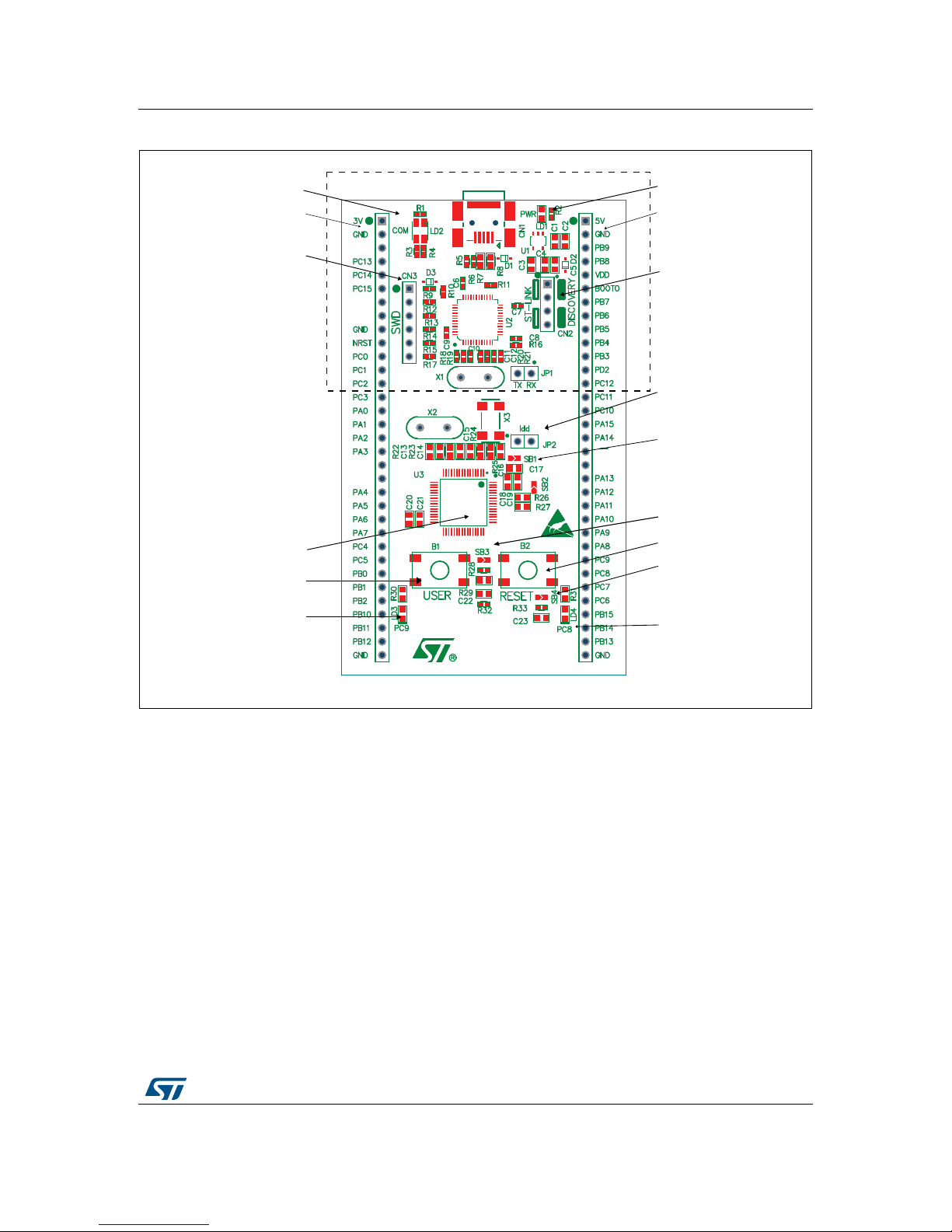
1. Check jumper position on the board, JP2 on, CN2 on (Discovery selected).
2. Connect the 32L100CDISCOVERY board to a PC with a USB cable ‘type A to mini-B’
through USB connector CN1 to power the board. Red LED LD1 (PWR) and LD2 (COM)
light up and green LED LD3 blinks.
3. Press user button B1 (bottom left corner of the board).
4. Observe how the green LED LD3 blinking changes according to USER button B1
clicks.
5. Each click on USER button B1 is confirmed by the blue LED LD4.
6. To study or modify the DISCOVER project related to this demo, visit
www.st.com/stm32l1-discovery and follow the tutorial.
7. Discover the STM32L100 Value Line features, download and execute programs
proposed in the list of projects.
8. Develop your own application using available examples.
2.2 System requirements
•Windows PC (XP, Vista, 7)
•USB type A to Mini-B USB cable
2.3 Development toolchain supporting the 32L100CDISCOVERY
•Altium®, TASKING™ VX-toolset
•ARM®, Atollic TrueSTUDIO®
•IAR™, EWARM (IAR Embedded Workbench®)
•Keil™, MDK-ARM™
2.4 Order code
To order the STM32L100 Value Line Discovery kit, use the order code STM32L100C-
DISCO.

DocID025091 Rev 1 7/30
UM1656 Features
29
3 Features
The 32L100CDISCOVERY kit offers the following features:
•STM32L100RCT6 microcontroller featuring 256 KB Flash, 16 KB RAM in an LQFP64
package
•On-board ST-LINK/V2 with selection mode switch to use the kit as a standalone
ST-LINK/V2 (with SWD connector for programming and debugging)
•Board power supply: through USB bus or from an external 5 V supply voltage
•External application power supply: 3 V and 5 V
•Four LEDs:
– LD1 (red) for 3.3 V power on
– LD2 (red/green) for USB communication
– LD3 (green) for PC9 output
– LD4 (blue) for PC8 output
•Two push buttons (user and reset)
•Extension header for LQFP64 I/Os for quick connection to prototyping board and easy
probing.
•An additional board is provided with the kit which can be connected to the extension
connector for even easier prototyping and probing.
•A large number of free ready-to-run application firmware examples are available on
www.st.com/stm32l1-discovery to support quick evaluation and development.

Hardware and layout UM1656
8/30 DocID025091 Rev 1
4 Hardware and layout
The 32L100CDISCOVERY is designed around the STM32L100RCT6 microcontroller in a
64-pin LQFP package.
Figure 2 illustrates the connections between the STM32L100RCT6 and its peripherals (ST-
LINK/V2, push button, LEDs and connectors).
Figure 3 and Figure 4 help you to locate these features on the 32L100CDISCOVERY.
Figure 2. Hardware block diagram
MS32775V1
LED
LD4, PC8
B1
USER
I/O
Embedded
ST-LINK/V2
Mini
USB
LED
LD3, PC9
B2
RST
RESET
I/OI/O
Header
Header
SWD
STM32L100RCT6

DocID025091 Rev 1 9/30
UM1656 Hardware and layout
29
Figure 3. Top layout
1. Pin 1 of CN2, CN3, P1 and P2 connectors are identified by a square.
MS32777V1
(red/green LED) LD2
COM
CN3
SWD connector
IDD measurement
ST-LINK/V2
B1 user button
B2 reset button
LD1 (red LED)
PWR
CN2
ST-LINK/DISCOVERY
selector
(green LED) LD3
LD4 (blue LED)
STM32L100RCT6
JP2
5V power supply
input/output
3V power supply
su
input/output
SB1 (VBAT)
SB3 (B1-USER)
SB4 (B2-RESET)
VLCD
GND
VDD
VDD
GND
MB1108 rev B
STM32L100C-DISCO
PH0
PH1
www.st.com/stm32l1-discovery

Hardware and layout UM1656
10/30 DocID025091 Rev 1
Figure 4. Bottom layout
SB6, SB8, SB10, SB12
MS30025V1
SB5, SB7, SB9, SB11
(RESERVED)
(DEFAULT)
SB20, SB21 (X3 crystal)
SB14, SB15 (RX, TX)
SB19 (NRST)
SB16, SB17 (X2 crystal)
SB13 (STM_RST)
SB22 (T_SWO)
SB18 (MCO)

DocID025091 Rev 1 11/30
UM1656 Hardware and layout
29
4.1 STM32L100RCT6 microcontroller
The Value Line STM32L100RCT6 incorporates the connectivity power of the universal serial
bus (USB) with the high-performance ARM Cortex™-M3 32-bit RISC core operating at a
32 MHz frequency, a memory protection unit (MPU), high-speed embedded memories
(256 Kbytes of Flash memory and 16 Kbytes of RAM) and an extensive range of enhanced
I/Os and peripherals connected to two APB buses.
The STM32L100RCT6 device offers one 12-bit ADC, two DACs, two ultra-low-power
comparators, six general-purpose 16-bit timers and two basic timers, which can be used as
time bases.
Moreover, the STM32L100RCT6 device contains standard and advanced communication
interfaces: two I2Cs, three SPIs, two I2S, three USARTs and a USB.
It also includes a real-time clock and a set of backup registers that remain powered in
Standby mode.
Finally, the integrated LCD controller has a built-in LCD voltage generator that allows you to
drive up to 8 multiplexed LCDs with contrast independent of the supply voltage.
The ultra-low-power STM32L100RCT6 operates from a 1.8 to 3.6 V power supply with
BOR. It is available in the -40 to +85 °C temperature range. A comprehensive set of power-
saving modes allows the design of low-power applications.
Figure 5. STM32L100RCT6 package
-36
34-,2#4
+BYTESOF&LASHMEMORY
+BYTESOF2!-
,1&0XMM

Hardware and layout UM1656
12/30 DocID025091 Rev 1
Figure 6. STM32L100RCT6 block diagram
EXT. IT
WKU P
WIn WATCH DOG
12bit ADC
JTAG & SW
20 AF
NJTRST
JTDI
JTCK/SWCLK
JTMS/SWDAT
JTDO
As AF
NRST
VDD = 1.8 V to 3.6 V
VSS
51 AF
USB 2.0 FS device USB_DP
SRAM 16K
2x(8x16bit)
fMAX :32 MHz
SCL,SDA,SMBus,PMBus
as AF
GP DMA 7 channels
XTAL OSC
1-24 MHz
AHPBCLK
APBPCLK
HCLK
FCLK
EEPROM 64 bit
VOLT. REG.
VDDC ORE POW ER
Backup interface
BusMatrix 5M/5S
Interface
Ibus
Dbus
obl
EE²
USB SRAM 512B
USART1
USART2
SPI2/I2S
5 x 32-Bit
backup
reg.
SCL,SDA as AF
I2C1
RX,TX,CTS,RTS,
SmartCard as AF
Standby
WDG32K
VDDA /
VSSA
RX,TX,CTS,
RTS,SmartCard
as AF
NVIC
SPI1
MOSI,MISO,
SCK,NSS
as AF
IF
interface
PVD
BOR
Int
RTC V2
AWU
System
PA[15:0]
PB[15:0]
PC[15:0]
PD[15:0]
LCD 8x28 (4x32) SEGx
COMx
12bit DAC1
FIFI
IF
DAC_OUT1 as AF
DAC_OUT2 as AF
MPU
Vref
GP Comp
BOR / Bgap
C O M Px_ IN x PU / PD
PDR
PDR
TIMER6
1 Channel
General purpose
timers
256 KB
PROGRAM
4 KB DATA
8 KB BOOT
LCDBooster
V
LCD
PH [2:0]
RCLSI
MOSI,MISO,SCK,NSS,
WS,CK,MCK,SD as AF
2x(8x16bit)
Supply
monitoring
@VDDA
Supply monitoring
MS32904V1
APB2: f
MAX
= 32MHz
PLL &
Clock
Mgmt
AHB/
APB2
AHB/
APB1
GPIO PORTC
GPIO PORTD
GPIO PORTH
APB1: f
MAX
= 32MHz
@VDDA
@VDDA
@VDD
@VDD
@VDD
@VDDA
@VDDA
TIMER7
TIMER2
TIMER3
TIMER4
VLCD = 2.5 V to 3.6 V
OSC32_IN
OSC32_OUT
RTC_OUT
OSC_IN
OSC_OUT
TAMPER
4 Channels
4 Channels
4 Channels
M3 CPU
GPIO PORTA
GPIO PORTB
AHB: f
MAX
= 32MHz
GP DMA2 5 channels
MOSI,MISO,SCK,NSS,
WS,CK,MCK,SD as AF
RX,TX,CTS,RTS,
SmartCard as AF
RCMSI
RCHSI
1 Channel
2 Channels
XTAL 32kHz
12bit DAC2
USB_DM
USART3
SPI3/I2S
I2C2
TIMER9
TIMER10
TIMER11

DocID025091 Rev 1 13/30
UM1656 Hardware and layout
29
4.2 Embedded ST-LINK/V2
The ST-LINK/V2 programming and debugging tool is integrated on the
32L100CDISCOVERY. The embedded ST-LINK/V2 can be used in 2 different ways
according to the jumper states (see Table 2):
•Program/debug the MCU on board,
•Program/debug an MCU in an external application board using a cable connected to
SWD connector CN3.
The embedded ST-LINK/V2 supports only SWD for STM32 devices. For information about
debugging and programming features refer to user manual UM1075 (ST-LINK/V2 in-circuit
debugger/programmer for STM8 and STM32) which describes in detail all the ST-LINK/V2
features.
Figure 7. Typical configuration
Table 2. Jumper states
Jumper state Description
Both CN2 jumpers ON ST-LINK/V2 functions enabled for on board programming (default)
Both CN2 jumpers OFF ST-LINK/V2 functions enabled for application through external CN3
connector (SWD supported)
-36
(ARDWAREREQUIREMENTS
53"CABLETYPE!TOMINI"
COMPUTERWITH7INDOWS806ISTAOR
$EVELOPMENTTOOLCHAIN
!LTIUM4!3+).'684OOLSET
!TOLLIC4RUE345$)/
)!2%7!2-
+EIL-$+!2-

Hardware and layout UM1656
14/30 DocID025091 Rev 1
4.2.1 Using ST-LINK/V2 to program/debug the STM32L100 Value Line
on board
To program the STM32L100 Value Line microcontroller on board, simply plug in the two
jumpers on CN2, as shown in Figure 8 in red, but do not use the CN3 connector as that
could disturb communication with the STM32L100RCT6 of the 32L100CDISCOVERY.
Figure 8. 32L100CDISCOVERY connections
-36
CN2 jumpers ON
CN3
SWD connector

DocID025091 Rev 1 15/30
UM1656 Hardware and layout
29
4.2.2 Using ST-LINK/V2 to program/debug an external STM32 application
It is very easy to use the ST-LINK/V2 to program the STM32 on an external application.
Simply remove the 2 jumpers from CN2 as shown in Figure 9, and connect your application
to the CN3 debug connector according to Table 3.
Note: SB19 and SB22 must be OFF if you use CN3 pin 5 in your external application.
Figure 9. ST-LINK connections
Table 3. Debug connector CN3 (SWD)
Pin CN3 Designation
1 VDD_TARGET VDD from application
2 SWCLK SWD clock
3 GND Ground
4 SWDIO SWD data input/output
5 NRST RESET of target MCU
6 SWO Reserved
-36
CN2 jumpers OFF
CN3
SWD connector

Hardware and layout UM1656
16/30 DocID025091 Rev 1
4.3 Power supply and power selection
The power supply is provided either by the host PC through the USB cable, or by an
external 5V power supply.
The D1 and D2 diodes protect the 5V and 3V pins from external power supplies:
•5V and 3V can be used as output power supplies when another application board is
connected to pins P1 and P2.
In this case, the 5V and 3V pins deliver a 5V or 3V power supply and power
consumption must be lower than 100 mA.
•5V can also be used as input power supplies e.g. when the USB connector is not
connected to the PC.
In this case, the 32L100CDISCOVERY board must be powered by a power supply unit
or by auxiliary equipment complying with standard EN-60950-1: 2006+A11/2009, and
must be Safety Extra Low Voltage (SELV) with limited power capability.
4.4 LEDs
•LD1 PWR: Red LED indicates that the board is powered.
•LD2 COM: Tricolor LED (COM) advises on the communication status as follows:
– Slow blinking Red LED/Off: At power on before USB initialization
– Fast blinking Red LED/Off: After the first correct communication between PC and
STLINK/V2 (enumeration)
– Red LED On: When initialization between PC and ST-LINK/V2 is successfully
finished
– Green LED On: After successful target communication initialization
– Blinking Red/Green LED: During communication with target
– Red LED On: Communication finished and OK
– Orange LED On: Communication failure
•User LD3: Green user LED connected to the I/O PC9 of the STM32L100RCT6.
•User LD4: Blue user LED connected to the I/O PC8 of the STM32L100RCT6.
4.5 Push buttons
•B1 USER: User push button connected to the I/O PA0 of the STM32L100RCT6.
•B2 RESET: Push button used to RESET the STM32L100RCT6.
4.6 JP2 (IDD)
Jumper JP2, labeled IDD, allows the consumption of STM32L100RCT6 to be measured by
removing the jumper and connecting an ammeter.
•Jumper on: STM32L100RCT6 is powered (default).
•Jumper off: an ammeter must be connected to measure the STM32L100RCT6 current,
(if there is no ammeter, the STM32L100RCT6 is not powered).

DocID025091 Rev 1 17/30
UM1656 Hardware and layout
29
4.7 Oscillator clock (OSC)
4.7.1 OSC clock supply
PH0 and PH1 can be used as GPIO or as HSE oscillator. By default these I/Os are
configured as GPIO, so SB16 and SB17 are closed, SB18 is open and R22, R23, C13 and
C14 are not populated.
An external HSE clock can be provided to the MCU in three ways:
•MCO from ST-LINK. From MCO of the STM32F103. This frequency cannot be
changed, it is fixed at 8 MHz and connected to PH0-OSC_IN of the STM32L100RCT6.
Configuration needed:
– SB16, SB18 CLOSED
– R22, R23 removed
– SB17 OPEN
•Oscillator onboard. From X2 crystal (not provided). For typical frequencies and its
capacitors and resistors, please refer to the STM32L100RCT6 Datasheet.
Configuration needed:
– SB16, SB17 SB18 OPEN
– R22, R23, C13, C14 soldered
•Oscillator from external PH0. From external oscillator through pin 7 of the P1
connector. Configuration needed:
– SB16, SB17 CLOSED
– SB18 OPEN
– R22 and R23 removed
4.7.2 OSC 32 KHz clock supply
PC14 and PC15 can be used as GPIO or as LSE oscillator. By default these I/Os are
configured as GPIO, so SB20 & SB21 are closed and X3, R24, R25 are not populated.
An external LSE clock can be provided to the MCU in two ways:
•Oscillator onboard. From X3 crystal (not provided). Configuration needed:
– SB20, SB21 OPEN
– C15, C16, R24 and R25 soldered.
•Oscillator from external PC14. From external oscillator trough the pin 5 of P1
connector. Configuration needed:
– SB20, SB21 CLOSED
– R24 and R25 removed

Hardware and layout UM1656
18/30 DocID025091 Rev 1
4.8 Solder bridges
Table 4. Solder bridge settings
Bridge State(1) Description
SB16,17
(X2 crystal)(2) OFF X2, C13, C14, R22 and R23 provide a clock. PH0, PH1 are disconnected
from P1.
ON PH0, PH1 are connected to P1 (R22, R23 and SB18 must not be fitted).
SB6,8,10,12 (Default) ON Reserved, do not modify.
SB5,7,9,11 (Reserved) OFF Reserved, do not modify.
SB20,21
(X3 crystal)
OFF X3, C15, C16, R24 and R25 deliver a 32 KHz clock. PC14, PC15 are not
connected to P1.
ON PC14, PC15 are only connected to P1 (R24, R25 must not be fitted).
SB4
(B2-RESET)
ON B2 push button is connected to the NRST pin of the STM32L100RCT6
MCU.
OFF B2 push button is not connected the NRST pin of the STM32L100RCT6
MCU.
SB3
(B1-USER)
ON B1 push button is connected to PA0.
OFF B1 push button is not connected to PA0.
SB1
(VBAT powered from VDD)
ON VBAT is permanently powered from VDD.
OFF VBAT is not powered from VDD but pin3 of P1.
SB14,15
(RX,TX)
OFF Reserved, do not modify.
ON Reserved, do not modify.
SB19
(NRST)
ON NRST signal of the CN3 connector is connected to the NRST pin of the
STM32L100RCT6 MCU.
OFF NRST signal of the CN3 connector is not connected to the NRST pin of the
STM32L100RCT6 MCU.
SB22
(T_SWO)
ON SWO signal of the CN3 connector is connected to PB3.
OFF SWO signal is not connected.
SB13
(STM_RST)
OFF No incidence on STM32F103C8T6 (ST-LINK/V2) NRST signal.
ON STM32F103C8T6 (ST-LINK/V2) NRST signal is connected to GND.
SB2
(BOOT0)
ON BOOT0 signal of the STM32L100RCT6 MCU is held low through a
510 Ohm pull-down resistor.
OFF BOOT0 signal of the STM32L100RCT6 MCU can be set high through a
10 K Ωpull-up resistor R27 to solder.
SB18
(MCO)(2) ON Provides the 8 MHz for OSC_IN from MCO of STM32L100RCT6.
OFF See SB16, SB17 description.
1. Default SBx state is shown in bold.
2. OSC_IN clock comes from MCO if SB18 is ON and SB16,17 are OFF
and comes from X2 if SB18 is OFF and SB16,17 are ON.

DocID025091 Rev 1 19/30
UM1656 Hardware and layout
29
4.9 Extension connectors
The male headers P1 and P2 can connect the 32L100CDISCOVERY to a standard
prototyping/wrapping board. STM32L100RCT6 GPI/Os are available on these connectors.
P1 and P2 can also be probed by an oscilloscope, logical analyzer or voltmeter.
Table 5. MCU pin description versus board function
MCU pin Board function
Main
function Alternate
functions
LQFP64
Push button
LED
SWD
OSC
Free I/O
Power supply
CN3
P1
P2
BOOT0 BOOT0 60 6
NRST NRST 7
RESET
NRST
510
PA0
WKUP1/RTC_TAMP2/
TIM2_CH1_ETR/
USART2_CTS/ADC_IN0/
COMP1_INP
14
USER
15
PA1 TIM2_CH2/USART2_RTS/
LCD_SEG0/ADC_IN1/
COMP1_INP/OPAMP1_VINP 15 16
PA2
TIM2_CH3/TIM9_CH1/
USART2_TX/LCD_SEG1/
ADC_IN2/COMP1_INP/
OPAMP1_VINM
16 17
PA3
TIM2_CH4/TIM9_CH2/
USART2_RX/LCD_SEG2/
ADC_IN3/COMP1_INP/
OPAMP1_VOUT
17 18
PA4
SPI1_NSS/SPI3_NSS/
I2S3_WS/USART2_CK/
ADC_IN4/DAC_OUT1/
COMP1_INP
20 21
PA5 TIM2_CH1_ETR/SPI1_SCK
/ADC_IN5/DAC_OUT2/
COMP1_INP 21 22
PA6
TIM3_CH1/TIM10_CH1/
SPI1_MISO/LCD_SEG3/
ADC_IN6/COMP1_INP/
OPAMP2_VINP
22 23

Hardware and layout UM1656
20/30 DocID025091 Rev 1
PA7
TIM3_CH2/TIM11_CH1/
SPI1_MOSI/LCD_SEG4/
ADC_IN7/COMP1_INP
/OPAMP2_VINM
23 24
PA8 USART1_CK/MCO/
LCD_COM0 41 25
PA9 USART1_TX/LCD_COM1 42 24
PA10 USART1_RX/LCD_COM2 43 23
PA11 USART1_CTS/USB_DM/
SPI1_MISO 44 22
PA12 USART1_RTS/USB_DP/
SPI1_MOSI 45 21
PA13 JTMS-SWDAT 46
SWDIO
420
PA14 JTCK-SWCLK 49
SWCLK
217
PA15 TIM2_CH1_ETR/SPI1_NSS
/SPI3_NSS/I2S3_WS/
LCD_SEG17 50 16
PB0
TIM3_CH3/LCD_SEG5/
ADC_IN8/COMP1_INP/
VREF_OUT/
OPAMP2_VOUT
26 27
PB1 TIM3_CH4/LCD_SEG6/
ADC_IN9/COMP1_INP/
VREF_OUT 27 28
PB2/BO
OT1 COMP1_INP 28 29
PB3 TIM2_CH2/SPI1_SCK/
SPI3_SCK/I2S3_CK/
LCD_SEG7/COMP2_INM 55
SWO
611
Table 5. MCU pin description versus board function (continued)
MCU pin Board function
Main
function Alternate
functions
LQFP64
Push button
LED
SWD
OSC
Free I/O
Power supply
CN3
P1
P2
Table of contents
Other ST Motherboard manuals

ST
ST EVAL-L9963-MCU Installation and operating instructions

ST
ST SPC560P-DISP User manual

ST
ST EVALSP1310CPU User manual

ST
ST STEVAL-BLUEMIC-1 User manual

ST
ST STEVAL-LLL014V1 User manual

ST
ST Nucleo STM32F302R8 User manual

ST
ST UM1935 User manual

ST
ST EVSPIN32G4-DUAL User manual

ST
ST STEVAL-ISB68RX User manual

ST
ST STM32100B-EVAL User manual