ST SPC560P-DISP User manual

May 2014 DocID026329 Rev 1 1/24
UM1762
User manual
SPC560P-DISP Discovery+ evaluation board
Introduction
The SPC560P-DISP Discovery kit helps you to discover SPC56 P line Power Architecture
®
Microcontrollers.
The discovery board is based on SPC560P50L5, 64 MHz, single issue, 32-bit CPU core
complex (e200z0h) CPU core with 574KB flash in an LQFP144 package.
The numerous interfaces including GPI/O's, peripherals such as CAN, JTAG, K-Line, LIN,
FlexCAN and GPIOs make the SPC560P-DISP an excellent starter kit for customer quick
evaluation and project development.
Dedicated connectors allow plugging Arduino shields (Arduino-compatible).
The SPC560 P line is designed to address cost sensitive chassis, airbag, electrical
hydraulic power steering (EHPS), electric power steering (EPS), and electrical motor control
applications.
Free ready-to-run application firmware examples are available inside SPC5Studio
(www.st.com/spc5studio) to support quick evaluation and development.
www.st.com
Downloaded from Arrow.com.

Contents UM1762
2/24 DocID026329 Rev 1
Contents
1 SPC560P-DISP Discovery+ board . . . . . . . . . . . . . . . . . . . . . . . . . . . . . . 5
1.1 Debug interface . . . . . . . . . . . . . . . . . . . . . . . . . . . . . . . . . . . . . . . . . . . . . 5
1.2 I/O interface and connectors . . . . . . . . . . . . . . . . . . . . . . . . . . . . . . . . . . . 5
2 Hardware overview . . . . . . . . . . . . . . . . . . . . . . . . . . . . . . . . . . . . . . . . . . 6
2.1 Power Supply section . . . . . . . . . . . . . . . . . . . . . . . . . . . . . . . . . . . . . . . . . 6
2.1.1 5 VDC power supply . . . . . . . . . . . . . . . . . . . . . . . . . . . . . . . . . . . . . . . . 7
2.1.2 3.3 VDC power supply . . . . . . . . . . . . . . . . . . . . . . . . . . . . . . . . . . . . . . 8
2.1.3 Power supply using USB connection . . . . . . . . . . . . . . . . . . . . . . . . . . . . 8
2.1.4 Automatic DC source selector . . . . . . . . . . . . . . . . . . . . . . . . . . . . . . . . . 9
2.2 Crystal oscillator . . . . . . . . . . . . . . . . . . . . . . . . . . . . . . . . . . . . . . . . . . . . . 9
2.3 Reset section . . . . . . . . . . . . . . . . . . . . . . . . . . . . . . . . . . . . . . . . . . . . . . 10
2.4 User LEDs . . . . . . . . . . . . . . . . . . . . . . . . . . . . . . . . . . . . . . . . . . . . . . . . 10
2.5 ADC reference . . . . . . . . . . . . . . . . . . . . . . . . . . . . . . . . . . . . . . . . . . . . . 10
2.6 Integrated USB programmer/debugger . . . . . . . . . . . . . . . . . . . . . . . . . . .11
2.7 JTAG connectors . . . . . . . . . . . . . . . . . . . . . . . . . . . . . . . . . . . . . . . . . . . 13
2.8 FlexCAN interface and Safety Port . . . . . . . . . . . . . . . . . . . . . . . . . . . . . 15
2.9 FlexRay interface . . . . . . . . . . . . . . . . . . . . . . . . . . . . . . . . . . . . . . . . . . . 15
2.10 LINFlex communication (Serial Communication Interface module) . . . . . 16
2.11 Connectors Arduino-compatible . . . . . . . . . . . . . . . . . . . . . . . . . . . . . . . . 17
2.12 I/O header . . . . . . . . . . . . . . . . . . . . . . . . . . . . . . . . . . . . . . . . . . . . . . . . 18
3 PCB layout . . . . . . . . . . . . . . . . . . . . . . . . . . . . . . . . . . . . . . . . . . . . . . . . 21
Appendix A General handling precautions . . . . . . . . . . . . . . . . . . . . . . . . . . . . . 22
Revision history . . . . . . . . . . . . . . . . . . . . . . . . . . . . . . . . . . . . . . . . . . . . . . . . . . . . 23
Downloaded from Arrow.com.

DocID026329 Rev 1 3/24
UM1762 List of tables
3
List of tables
Table 1. PSU Section - LEDs . . . . . . . . . . . . . . . . . . . . . . . . . . . . . . . . . . . . . . . . . . . . . . . . . . . . . . . 7
Table 2. User LEDs . . . . . . . . . . . . . . . . . . . . . . . . . . . . . . . . . . . . . . . . . . . . . . . . . . . . . . . . . . . . . 10
Table 3. JTAG connector (X1 and X2) . . . . . . . . . . . . . . . . . . . . . . . . . . . . . . . . . . . . . . . . . . . . . . . 14
Table 4. I/O header (Schematic diagram). . . . . . . . . . . . . . . . . . . . . . . . . . . . . . . . . . . . . . . . . . . . . 19
Table 5. Document revision history . . . . . . . . . . . . . . . . . . . . . . . . . . . . . . . . . . . . . . . . . . . . . . . . . 23
Downloaded from Arrow.com.

List of figures UM1762
4/24 DocID026329 Rev 1
List of figures
Figure 1. SPC560P-DISP Discovery+ board . . . . . . . . . . . . . . . . . . . . . . . . . . . . . . . . . . . . . . . . . . . . 5
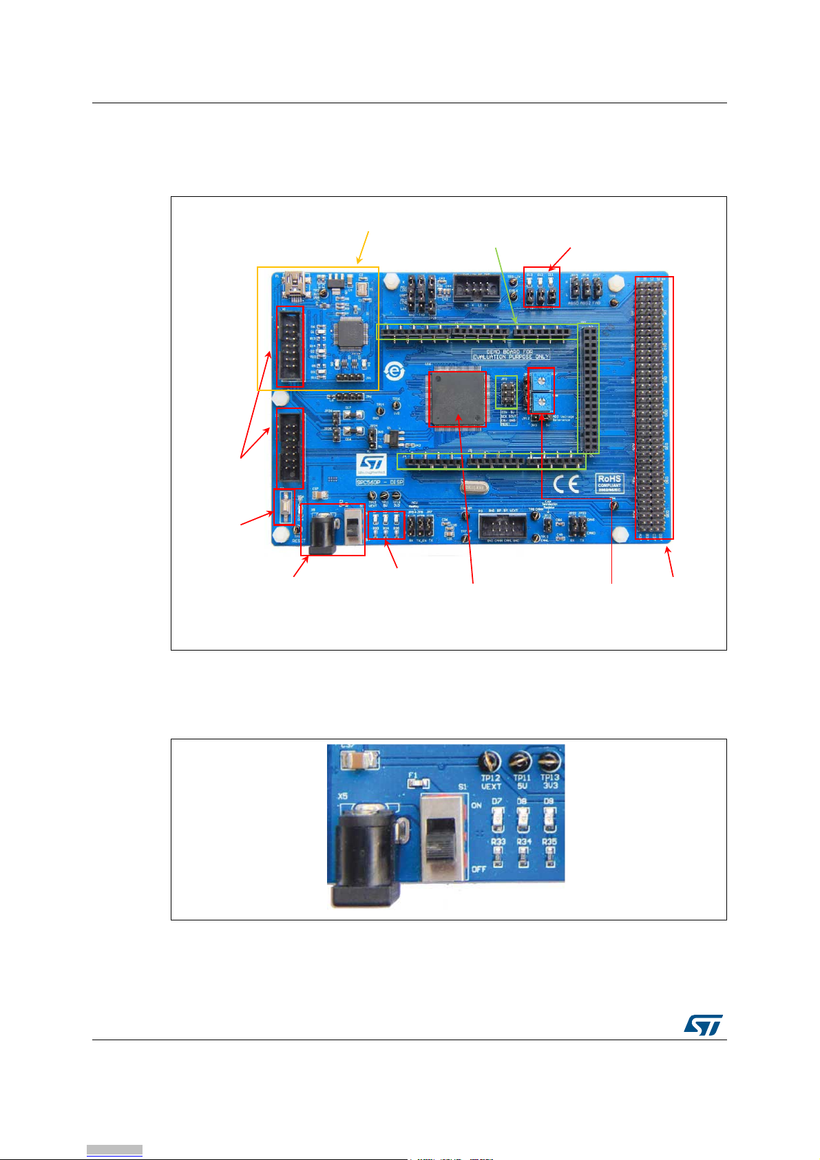
Figure 2. SPC560P-DISP - hw overview . . . . . . . . . . . . . . . . . . . . . . . . . . . . . . . . . . . . . . . . . . . . . . . 6
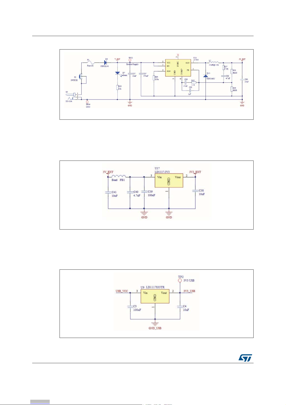
Figure 3. PSU section (PCB top side) . . . . . . . . . . . . . . . . . . . . . . . . . . . . . . . . . . . . . . . . . . . . . . . . . 6
Figure 4. PSU section (PCB bottom side) . . . . . . . . . . . . . . . . . . . . . . . . . . . . . . . . . . . . . . . . . . . . . . 7
Figure 5. PSU section (Vout: 5.0 V
DC
). . . . . . . . . . . . . . . . . . . . . . . . . . . . . . . . . . . . . . . . . . . . . . . . . 8
Figure 6. PSU section (Vout: 3.3 V
DC
). . . . . . . . . . . . . . . . . . . . . . . . . . . . . . . . . . . . . . . . . . . . . . . . . 8
Figure 7. USB connection - 3.3 V
DC. . . . . . . . . . . . . . . . . . . . . . . . . . . . . . . . . . . . . . . . . . . . . . . . . . . . . . . . . . . . . . . .8
Figure 8. Automatic DC source selector . . . . . . . . . . . . . . . . . . . . . . . . . . . . . . . . . . . . . . . . . . . . . . . 9
Figure 9. Crystal oscillator . . . . . . . . . . . . . . . . . . . . . . . . . . . . . . . . . . . . . . . . . . . . . . . . . . . . . . . . . . 9
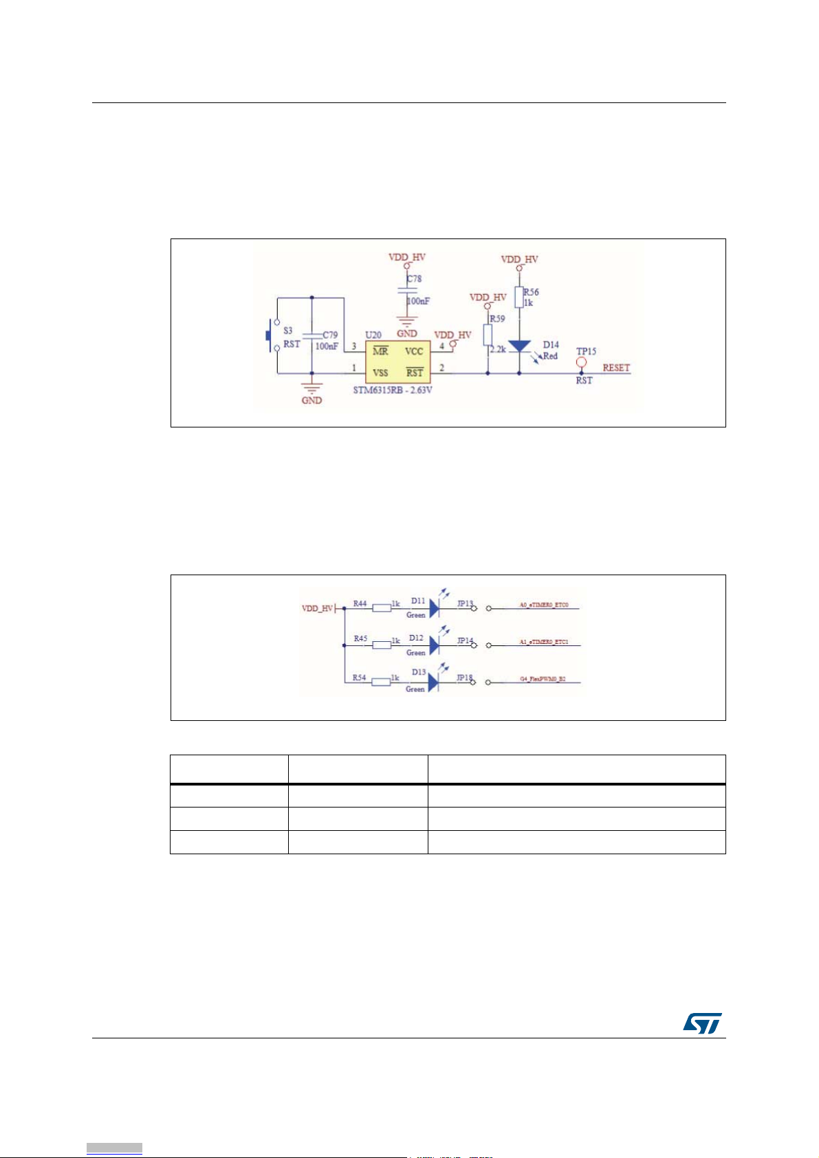
Figure 10. Reset section . . . . . . . . . . . . . . . . . . . . . . . . . . . . . . . . . . . . . . . . . . . . . . . . . . . . . . . . . . . 10
Figure 11. User LEDs . . . . . . . . . . . . . . . . . . . . . . . . . . . . . . . . . . . . . . . . . . . . . . . . . . . . . . . . . . . . . 10
Figure 12. ADC reference . . . . . . . . . . . . . . . . . . . . . . . . . . . . . . . . . . . . . . . . . . . . . . . . . . . . . . . . . . 11
Figure 13. Integrated debugger – USB input . . . . . . . . . . . . . . . . . . . . . . . . . . . . . . . . . . . . . . . . . . . . 12
Figure 14. Integrated debugger – EEPROM . . . . . . . . . . . . . . . . . . . . . . . . . . . . . . . . . . . . . . . . . . . . 12
Figure 15. Integrated debugger - Level Shifters . . . . . . . . . . . . . . . . . . . . . . . . . . . . . . . . . . . . . . . . . 13
Figure 16. Integrated debugger - LEDs . . . . . . . . . . . . . . . . . . . . . . . . . . . . . . . . . . . . . . . . . . . . . . . . 13
Figure 17. JTAG connectors . . . . . . . . . . . . . . . . . . . . . . . . . . . . . . . . . . . . . . . . . . . . . . . . . . . . . . . . 14
Figure 18. FlexCAN - jumpers configuration . . . . . . . . . . . . . . . . . . . . . . . . . . . . . . . . . . . . . . . . . . . . 15
Figure 19. High Speed CAN and FlexRay . . . . . . . . . . . . . . . . . . . . . . . . . . . . . . . . . . . . . . . . . . . . . . 15
Figure 20. FlexRay – jumper configuration . . . . . . . . . . . . . . . . . . . . . . . . . . . . . . . . . . . . . . . . . . . . . 16
Figure 21. FlexRay transceiver and connector . . . . . . . . . . . . . . . . . . . . . . . . . . . . . . . . . . . . . . . . . . 16
Figure 22. LINFlex communication (I) . . . . . . . . . . . . . . . . . . . . . . . . . . . . . . . . . . . . . . . . . . . . . . . . . 17
Figure 23. LINFlex communication (I) . . . . . . . . . . . . . . . . . . . . . . . . . . . . . . . . . . . . . . . . . . . . . . . . . 17
Figure 24. Connectors Arduino-compatible (I). . . . . . . . . . . . . . . . . . . . . . . . . . . . . . . . . . . . . . . . . . . 17
Figure 25. Connectors Arduino-compatible (II) . . . . . . . . . . . . . . . . . . . . . . . . . . . . . . . . . . . . . . . . . . 18
Figure 26. Connectors Arduino-compatible (III). . . . . . . . . . . . . . . . . . . . . . . . . . . . . . . . . . . . . . . . . . 18
Figure 27. Connectors Arduino-compatible (IV). . . . . . . . . . . . . . . . . . . . . . . . . . . . . . . . . . . . . . . . . . 18
Figure 28. I/O header (Schematic diagram). . . . . . . . . . . . . . . . . . . . . . . . . . . . . . . . . . . . . . . . . . . . . 19
Figure 29. PCB layout . . . . . . . . . . . . . . . . . . . . . . . . . . . . . . . . . . . . . . . . . . . . . . . . . . . . . . . . . . . . . 21
Downloaded from Arrow.com.

DocID026329 Rev 1 5/24
UM1762 SPC560P-DISP Discovery+ board
23
1 SPC560P-DISP Discovery+ board
Figure 1. SPC560P-DISP Discovery+ board
The PCB, the components and all HW parts assembled in the board meet requirements of
the applicable RoHS directives.
1.1 Debug interface
•Double 2x7-pin JTAG interfaces
•USB mini B and integrated programmer/debugger
1.2 I/O interface and connectors
•PSU plug (+12V)
•FlexCAN interface
•FlexRay
•K-Line
•LINFlex
•Arduino connectors (Arduino compatibility)
•4x37 headers
("1(3*
Downloaded from Arrow.com.

Hardware overview UM1762
6/24 DocID026329 Rev 1
2 Hardware overview
Figure 2. SPC560P-DISP - hw overview
2.1 Power Supply section
Figure 3. PSU section (PCB top side)
63&3/
[+HDGHU
8VHU/('V
5HVHW
-7$*FRQQHFWRU
9
'&
SRZHU6XSSO\
DQGVZLWFK 3RWHQWLRPHWHU
IRU$'&
8VHU/('V
368DQG
9/('V
,QWHJUDWHG
SURJUDPPHUGHEXJJHU
("1(3*
("1(3*
Downloaded from Arrow.com.

DocID026329 Rev 1 7/24
UM1762 Hardware overview
23
Figure 4. PSU section (PCB bottom side)
2.1.1 5 V
DC
power supply
This section is only used when an external 12V PSU is connected to the X5 DC port
(a)
(X5).
The diode D6 is used to protect the board against reverse polarity and AC source. The fuse
F1 protects the board when an accidental short circuit occurs.
The LED D7 is switched on when the board is correctly powered and the switch S1 is set to
ON position.
The 5V generator is based on the ST device A7985; Figure 5 shows the circuit diagram.
Table 1. PSU Section - LEDs
Item Color Function
D7 Green Vext (+12V)
D8 Green 5V
D9 Green 3.3V
D3 Green VCIO
96XSSO\
8
96XSSO\
8
'&VRXUFH6HOHFWRU
88
("1(3*
a. The external 12V PSU adapter is not included in the evaluation kit
Downloaded from Arrow.com.

Hardware overview UM1762
8/24 DocID026329 Rev 1
Figure 5. PSU section (Vout: 5.0 V
DC
)
2.1.2 3.3 V
DC
power supply
The liner regulator LD1117-3V3 is used to generate the 3.3 V supply voltage; Figure 6
shows the schematic diagram.
Figure 6. PSU section (Vout: 3.3 V
DC
)
2.1.3 Power supply using USB connection
The board can be supplied by the USB cable when the internal programmer/debugger is
used; in this working condition 3.3 V is generated using a liner regulator (Figure 7).
Figure 7. USB connection - 3.3 V
DC
("1(3*
("1(3*
("1(3*
Downloaded from Arrow.com.

DocID026329 Rev 1 9/24
UM1762 Hardware overview
23
2.1.4 Automatic DC source selector
The circuit in Figure 8 switches 5 V and 3.3 V automatically when the board is supplied by
an external PSU or by 5V from the PC/USB cable. The voltage divider made by R46 and
R51 is used to sense the presence of an external PSU (5V is sensed) and it drives U19 and
U23 properly.
Figure 8. Automatic DC source selector
The jumper JP24 allows selecting the VDD_HV level: 3.3 V or 5 V.
2.2 Crystal oscillator
The SPC560P-DISP board is populated with 16 MHz crystal to clock the SPC560P50L5.
Figure 9. Crystal oscillator
("1(3*
("1(3*
Downloaded from Arrow.com.

Hardware overview UM1762
10/24 DocID026329 Rev 1
2.3 Reset section
The reset circuit (see Figure 10) generates a sharp signal to reset the microcontroller. The
core of the circuit is the device STM6315RB-2.63 V; it produces the reset pulse when the S3
button is pushed: D14 is turned on on when the reset pulse is generated.
Figure 10. Reset section
2.4 User LEDs
On the board are present three USER LEDs connected as shown in Figure 11. The jumpers
JP13, JP14 and JP18 allow disconnecting the LED cathodes and used the GPIO to a
different purpose.
Figure 11. User LEDs
2.5 ADC reference
Jumper JP 12 allows setting the ADC reference level: 5 V or 3.3 V.
("1(3*
Table 2. User LEDs
Item Color µC Pin - function
D11 Green A0_eTIMER0_ETC0
D12 Green A1_eTIMER0_ETC1
D13 Green G4_FlexPWM0_B2
("1(3*
Downloaded from Arrow.com.

DocID026329 Rev 1 11/24
UM1762 Hardware overview
23
Figure 12. ADC reference
Two potentiometers (R56 and R57) and the jumpers JP19 and JP20 allow the user to
quickly evaluate the performance of ADC: the analog voltage can be adjusted in the range is
0 ÷ VDD_HV_ADC.
Removing the jumper the pin E0 and E12 can be used to support a different application.
2.6 Integrated USB programmer/debugger
The integrated debugger, based on the device FTDI2232H and UDE PLS software, allows
the user to build, run and debug the software applications.
The integrated debugger can be configured to operate as standalone unit and used to
program and debug another SPC5xx application or an evaluation boards. The board is
configured to operate using the integrated debugger.
The SPC560P-DISP discovery board includes a full-featured, perpetual code-limited (128
Kbytes) PLS software license. The debugger serial number is reported on a label applied on
the board.
To download the debugger software and to activate license go to the PLS website.
The integrated debugger is accessible via ST's free integrated development environment,
SPC5Studio (www.st.com/spc5studio).
("1(3*
Downloaded from Arrow.com.

DocID026329 Rev 1 13/24
UM1762 Hardware overview
23
Figure 15. Integrated debugger - Level Shifters
Figure 16. Integrated debugger - LEDs
2.7 JTAG connectors
The integrated debugger can also be used as standalone debugger. To make possible this
functionality, two HW options are possible:
1. Remove the debugger for the main board cutting small portions of PCB where is
located the debugger; (cutable PCB).
2. Let the integrated PLS adapter on the board and electrically disconnect the adapter to
the microcontroller
The first option consists to remove the portion of PCB where is assembled the debugger
cutting small portion of PCB. Both the debugger and the discovery board do notneed HW
modification to work properly
(b)
. A JTAG connector (X1) present in the detached
debugger/programmer allows connecting the board to a target application. Level shifters are
("1(3*
("1(3*
b. Removing the integrated adapter the discovery board must be supplied using a PSU
Downloaded from Arrow.com.

Hardware overview UM1762
14/24 DocID026329 Rev 1
present to equalize the I/O levels. The discovery board can be programmed using an
external programmer connected to the JTAG X2.
The second solution does not need to remove the debugger because it can be disconnected
electrically removing the array resistor RP1. The two JTAG connectors allow connecting the
programmer to the target application. The discovery board must be supplied using a PSU
and a programmer must be connected to the JTAG port to program the microcontroller.
Figure 17. JTAG connectors
Table 3. JTAG connector (X1 and X2)
Pin Signal Pin Signal
1 TDI 2 GND
3 TDO 4 GND
5 TCK 6 GND
7 EVTI 8 NC
9 RESET 10 TMS
11 VDDE7 12 GND
13 RDY 14 JCOMP
("1(3*
Downloaded from Arrow.com.

DocID026329 Rev 1 15/24
UM1762 Hardware overview
23
2.8 FlexCAN interface and Safety Port
SPC560P50L5 includes a FlexCAN interface controller (version 2.0B), the transceiver and a
connector.
The controller also includes a second CAN controller synthesized to run at high bit rates to
be used as a safety port. It can be used as a second independent CAN module.
JP22 and JP23 allow selecting the CAN channel connected to the transceiver; see
Figure 18. JP10 connects the 120 Ωtermination resistor (the resistor is connected when the
jumper is present).
Figure 18. FlexCAN - jumpers configuration
The CAN output signals are available in a single 2x8 pin male connector (see U24 in
Figure 19); the FlexCAN output signals are connected to the even pins of the connector.
Figure 19. High Speed CAN and FlexRay
2.9 FlexRay interface
The FlexRay module implements the Protocol Specification 2.1 with selectable single or
dual channel support. The transceiver used is TJA1080 (U15); JP7, JP8 and JP9 allow
configuring the FlaxRay signals connected to the transceiver. The output signals are located
in the same connector used for the FlexCAN, the odd pins are used.
("1(3*
("1(3*
Downloaded from Arrow.com.

Hardware overview UM1762
16/24 DocID026329 Rev 1
Figure 20. FlexRay – jumper configuration
Figure 21. FlexRay transceiver and connector
2.10 LINFlex communication (Serial Communication Interface
module)
The LINFlex supports LIN Master mode, LIN Slave mode and UART mode. LIN state
machine is compliant to LIN1.3, 2.0, and 2.1 specifications.
Figure 22 and Figure 23 show the hardware implemented for the UART/LIN: U18 and U14
are the LIN and the K-Line transceivers respectively.
JP4 and JP5 configure UART or LIN; the RX and SX signals are available on the connector
JP6.
("1(3*
("1(3*
Downloaded from Arrow.com.

DocID026329 Rev 1 17/24
UM1762 Hardware overview
23
Figure 22. LINFlex communication (I)
Figure 23. LINFlex communication (I)
2.11 Connectors Arduino-compatible
In this discovery board are present Arduino compatible: the connectors J1 J2, J4 and J5 are
compatible with the Arduino-UNO shields and the J5, J6, and JP2 are compatible with
Arduino-Mega shields.
The figures here below are showing the connections of the microcontroller pins and the
Arduino connectors.
Figure 24. Connectors Arduino-compatible (I)
("1(3*
("1(3*
("1(3*
Downloaded from Arrow.com.

Hardware overview UM1762
18/24 DocID026329 Rev 1
Figure 25. Connectors Arduino-compatible (II)
Figure 26. Connectors Arduino-compatible (III)
Figure 27. Connectors Arduino-compatible (IV)
2.12 I/O header
All of the MCU GPIOs and communication channels can be accessed through a 4x37 I/O
headers. Here below the I/O header pin mapping summarized in .
("1(3*
("1(3*
("1(3*
Downloaded from Arrow.com.

DocID026329 Rev 1 19/24
UM1762 Hardware overview
23
Figure 28. I/O header (Schematic diagram)
Table 4. I/O header (Schematic diagram)
Pin
number ABCD
1GND GND GND +5V
2 D14_FlexPWM0_B1 G4_FlexPWM0_B2 E0_ADC1_AN5 E12_ADC1_AN10
3 G7_FlexPWM0_B3 D11_FlexPWM0_B0 C0_ADC1_AN3 E11_ADC1_AN9
4 B14_ADC1_AN1 E10_ADC1_AN8 B15_ADC1_AN2 E9_ADC1_AN7
5 E8_ADC1_AN6 D15_ADC1_AN4 -- E13_DSPI3_SCK
6G8_FlexPWM0_FAU
LT0 G9_FlexPWM0_FAU
LT1 E14_DSPI3_SOU
TE15_DSPI3_SIN
7G10_FlexPWM0_FA
ULT2 G11_FlexPWM0_FA
ULT3 -- --
8 F0_FlexRay0_DBG0 F1_FlexRay0_DBG1 -- --
9 C10_DSPI2_CS2 A9_DSPI2_CS1 -- C15_FlexRay0_CA_T
R_EN
10 A10_DSPI2_CS0 A11_DSPI2_SCK -- D0_FlexRay0_CA_TX
11 A12_DSPI2_SOUT A13_DSPI2_SIN B2_LIN0_TXD B3_LIN0_RXD
12 RESET -- -- --
13 -- -- -- --
14 G0_FCU0_F0 -- NMI D1_FlexRay0_CA_RX
("1(3*
Downloaded from Arrow.com.

Hardware overview UM1762
20/24 DocID026329 Rev 1
15 A5_DSPI1_CS0 A6_DSPI1_SCK B1_CAN0_RXD D2_FlexRay0_CB_RX
16 A7_DSPI1_SOUT A8_DSPI1_SIN A15_SafetyPort0_
RXD D3_FlexRay0_CB_TX
17 B0_CAN0_TXD A14_SafetyPort0_TX
DC12_eTIMER0_ET
C5 D4_FlexRay0_CB_TR
_EN
18 D12_FlexPWM0_X1 G2_FlexPWM0_X2 A0_eTIMER0_ET
C0 A2_eTIMER0_ETC2
19 G5_FlexPWM0_X3 D9_FlexPWM0_X0 A1_eTIMER0_ET
C1 A4_eTIMER1_ETC0
20 C9_DSPI2_CS3 -- F11_NEXUS0_EV
TI D8_DSPI1_CS2
21 F15_LIN1_RXD F14_LIN1_TXD F10_NEXUS0_EV
TO C4_DSPI0_CS0
22 D13_FlexPWM0_A1 G3_FlexPWM0_A2 A3_eTIMER0_ET
C3 G1_FCU0_F1
23 G6_FlexPWM0_A3 D10_FlexPWM0_A0 C11_eTIMER0_ET
C4 C13_eTIMER1_ETC1
24 F2_FlexRay0_DBG2 F3_FlexRay0_DBG3 F9_NEXUS0_MSE
O0 C14_eTIMER1_ETC2
25 D7_DSPI1_CS3 C8_DSPI1_CS1 B6_CLKOUT C5_DSPI0_SCK
26 B7_ADC0_AN0 B12_ADC0/1_AN14 C6_DSPI0_SOUT C7_DSPI0_SIN
27 B13_ADC1_AN0 B11_ADC0/1_AN13 C3_DSPI0_CS1 F12_eTIMER1_ETC3
28 B10_ADC0/1_AN12 B9_ADC0/1_AN11 D6_DSPI0_CS2 F13_eTIMER1_ETC4
29 E2_ADC0_AN5 E7_ADC0_AN10 D5_DSPI0_CS3 F8_NEXUS0_MSEO1
30 B8_ADC0_AN1 E6_ADC0_AN9 F7_NEXUS0_MC
KO F6_NEXUS0_MDO1
31 C2_ADC0_AN3 E5_ADC0_AN8 F5_NEXUS0_MD
O2 F4_NEXUS0_MDO3
32 E4_ADC0_AN7 C1_ADC0_AN2 GND GND
33 E3_ADC0_AN6 E1_ADC0_AN4 +5V 5V
34 GND GND GND 5V
35 -- -- -- --
36 -- -- -- --
37 V_EXT_P V_EXT_P 3v3 VDD_LV_COR
Table 4. I/O header (Schematic diagram) (continued)
Pin
number ABCD
Downloaded from Arrow.com.
Table of contents
Other ST Motherboard manuals

ST
ST STM32CubeF4 User manual

ST
ST X-NUCLEO-IDW01M1 User manual

ST
ST STM32MP157D-EV1 User manual

ST
ST STEVAL-ISF003V1 User manual

ST
ST EVAL-L99DZ200 User manual

ST
ST STEVAL-IHM020V1 User manual

ST
ST UM2248 User manual

ST
ST STEVAL-PCC008V1 User manual

ST
ST STM32 Nucleo User manual

ST
ST STEVAL-ISC004V1 User manual