1Getting started
1.1 System requirements
To test the board, the necessary hardware is:
• An isolated power supply with 5 V, 100 mA capability
• A power supply with 3.3 V to 5 V, 50 mA capability
• A clock generator capable of producing a square wave with frequency from 5 MHz to 25 MHz, TTL-level (0 –
3 V) for the ISOSD61 device
• A clock generator capable to produce two complementary square waves with frequency from 5 MHz to 25
MHz, LVDS-level (1.2 V common mode voltage, +-0.3 V differential voltage) for the ISOSD61L device
• An analog signal source (differential or single-ended) to be applied to the analog input(s) or a current to be
measured through a current shunt
• A digital equipment (PC, FPGA board, MCU board…) capable of implementing a digital filtering of the
sigma-delta modulated output.
1.2 Connecting the board
Follow the steps below to run it:
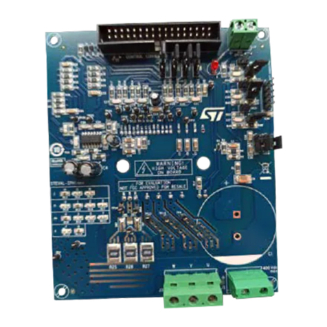
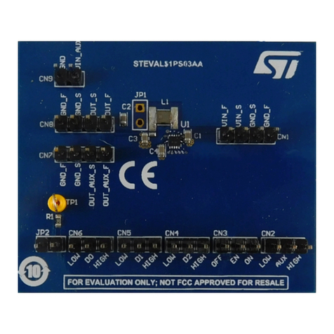
• Use the two twin-screw green connectors to supply 5 V to the isolated front end (VDDiso, M1) and 3.3 V to
5 V to the digital interface (VDD, M2). Carefully respect the polarity. Reversing the polarity may damage the
device.
• Connect the clock source and the data output to the on-board SMB connectors, respectively. Alternatively,
header pin connectors can be used. According to the device interface type:
– ISOSD61 (TTL): connect the clock generator to the MCLKIN connector (BNC2, or J2 and J5) and the
data cable to the MDAT connector (BNC4 or P1). Ensure the voltage amplitude is TTL-level compliant.
– ISOSD61L (LVDS): connect the clock paired cables to the MCLKIN+ and MCLKIN- connectors (BNC2
and BNC3, or J2, J4 and J5) and the data paired cables to the MDAT+ and MDAT- connectors
(BNC4 and BNC5, or P1 and P2). Ensure that levels and polarity are LVDS-level compliant and they
are adjusted to the on-board 110 ohm differential termination resistors. In the case of MDAT signals
terminated to the end of the line to the digital equipment, remove the MDAT termination resistor
opening the S3 and S4 soldered short-circuit pads.
– In case of using the header pin connectors, identify the right GND reference pin (J5 for the clock
signals and pin # 2 of P1 and P2 for the data signals)
• About the analog input signal, different options are possible:
– If a shunt is connected, the current to be sensed will be converted to a voltage signal and fed directly
to the analog inputs. No additional connections are required. Ensure not to exceed the current and
power ratings of the shunt. (Note: The board is designed to fit a BKW-M-R0003-5.0 shunt made by
Isabellenhütte Heusler. It’s rated 0.3 milliohm, 100 A max., 3 W max.)
– In the case of a single-ended analog input signal, place a jumper cap to the J11 2-pin header and
connect the signal cable to the VIN+ SMA on-board connector (BNC1). The maximum signal amplitude
is 640 mVp-p.
– In the case of a differential analog input signal, connect the paired cables to the VIN+ and VIN- (BNC1
and BNC6) SMA on-board connectors. Ensure the J10 and J11 pin headers are free from jumper caps.
1.3 Sigma-Delta data processing
The MDAT, 1-bit sigma-delta stream must be converted to an N-bit digital information in order to provide a high
resolution accurate digital representation of the sampled analog signal. This conversion process is the so-called
digital decimation filtering process. Among the various different decimation techniques, the use of a Sinc3 digital
filter is recommended because of its reasonable stopband attenuation combined with its quick step response.
The code below is an example of a generic Sinc3 filter written for GNU Octave that can be easily ported to other
languages or systems:
UM2815
Getting started
UM2815 - Rev 3 page 2/9
