ST STEVAL-AETKT2V1 User manual

Introduction
The STEVAL-AETKT2V1 evaluation kit implements bidirectional current sense amplifiers by placing a sense resistor either in
the high side or in the low side.
The STEVAL-AETKT2V1 kit consists of a mother board and two different daughter boards for different gain configurations.
TSC21x family implements zero drift technology and is specially designed to accurately measure current by amplifying the
voltage across a shunt resistor connected to its input. The voltage drop (Vsense) is then amplified by an amplifier.
Thanks to the use of thin film resistors, TSC21x offers an extremely precise gain and very high CMRR performance.
Moreover, thanks to the possibility of fixing the output common mode voltage through a reference pin, the TSC21x can be either
used as unidirectional or bidirectional current sensing amplifier.
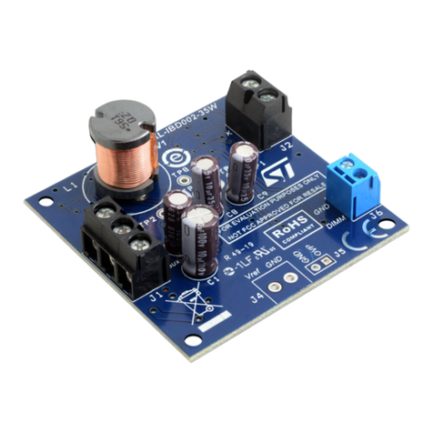
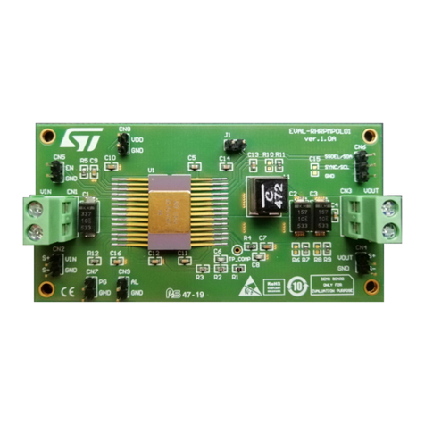
Figure 1. STEVAL-AETKT2V1 evaluation kit
Getting started with the STEVAL-AETKT2V1 evaluation kit for high precision
bidirectional current sense amplifiers
UM2859
User manual
UM2859 - Rev 1 - June 2021
For further information contact your local STMicroelectronics sales office.
www.st.com

1Getting started
1.1 Overview
• Input common mode voltage: 26 V
• Offset voltage: ±35 μV (±100 μV) max.
• Offset drift: 0.1 µV/°C max.
• Gain drift: 20 ppm/°C max.
• 2.7 to 26 V supply voltage
• Quiescent current: 100 μA max.
• SC70-6 and QFN10 (1.8 x 1.4 mm) package
• Temperature range: -40 to 125°C
• Gain configuration from 50 V/V to 1000 V/V
• RoHS compliant
1.2 Shunt resistance
The STEVAL-AETKT2V1 offers the possibility of soldering a shunt resistance directly on the PCB. The board can
host standard 2512 package size shunts on 4 W footprint optimized for minimal reading error.
You can choose the appropriate shunt package and value for your own application. If the chosen shunt is not
compatible with the footprint, it has be connected outside the evaluation kit.
The selection of the shunt resistor is a tradeoff between dynamic range and power dissipation. Generally, in high
current sensing applications, the focus is to reduce as much as possible the power dissipation (I²R) by choosing a
shunt with the smallest value.
The recommended shunt value is obtained from the following equation:
Rsense =VoutMax − Vol
Gain ⋅ 1+Errorgain
−2⋅ Vio ⋅1
Irange (1)
Where VoutMax is the maximum output voltage usually equal to the device VCC or the ADC connected to the
output, Vol is the output low swing value for the TSC21x family (in this case, it is 30 mV), Gain is the gain of the
selected device (for example, TSC213 has a gain of 50), ERRORgain equals to 1%, Vio represents the input offset
voltage (100 µV can be considered for TSC213), Irange is the actual range to be measured.
Note: It is recommended to take a bit smaller shunt value to have some margin and prevent saturation.
The actual current range is calculated by the following equations:
ImaxPositive =VoutMax − Vref
RSℎunt ⋅ Gain (2)
ImaxNegative =Vref − VoutMin
RSℎunt ⋅ Gain (3)
Table 1. Examples of current ranges with 3mOhm shunt over different gain, VCC and Vref values
Device VCC (V) Vref (V) Range Ipositive (A) Range INegative (A)
TSC213
3.3 2.5 4.66 -16
5 2.5 16 -16
TSC210
3.3 2.5 1.16 -4
5 2.5 4 -4
UM2859
Getting started
UM2859 - Rev 1 page 2/12

1.3 Connection
The STEVAL-AETKT2V1 evaluation kit can be connected to the application design via J1 header.
Table 2. J1 pin-out description
J1 pin Description
REF Output or input voltage reference (see Section 1.4 Voltage reference settings)
VCC Supply voltage
GND Ground
OUT TSC21x analog output value
1.4 Voltage reference settings
As the TSC21x family devices can measure current in both directions, some voltage reference has to be provided.
Voltage reference can be generated directly on the STEVAL-AETKT2V1 evaluation kit by a precision op-amp or
by shunt voltage reference. Another option is to use an external reference voltage source.
Refer to the following table for proper jumper settings.
Important: Only one jumper at a time can be placed on the kit.
Table 3. Voltage reference J2A and J2B jumper settings
J2A J2B Functionality
NA GND Unidirectional
NA VCC Unidirectional Inverted
REF1 NA Vref generated by op-amp TSB711 (default Vcc/2)(1)
REF2 NA Vref generated by shunt reference TS431 (default 1.24V)(1)
REF1 or REF2 GND or VCC Not allowed(2)
NA NA External voltage reference provided from J1
1. The reference voltage value can be adjusted by resistor values.
2. IC components might be damaged
UM2859
Connection
UM2859 - Rev 1 page 3/12

2Schematic diagrams
Figure 2. STEVAL-AETKT2V1 main board (STEVAL-AET011V1B) circuit schematic
The STEVAL-AET011V1B board is not available for separate sale
GND
VCC
GND
GND
GND
GND
REF
Out
REF
OutVo
Vin+
Vin- GND
VCC
GND
VCC
GND
VCC
VCC
GND
REF_1
VCC
GND
REF_2
REF_1
REF
REF_2
VCC
Vin+
Vin-
Vo
GND
GND
GND
D3
SMA4F18A
D4
SMA4F18A
Mini spring socket for Daughter Board
REF
1
2
P1
TERMINAL
R4
100k
R5
100k
R1
0R
R2
0R
R3
1k
C1
1µF
C2
100nF
C7
100pF
C3
1nF
C4
NC
C5
NC
C6
NC
D2
BAT54S
IN-
5
IN+
4
OUT 6
REF 1
VCC 3
GND
2
U1
TSC21x
J2B
J2A
J1
R8
NC
R7
0R
R6
2k
D5
TS431
V+
V-
3
4
1
25
U3
TSB711
D1
SMA4F18A
IN-
5
IN+
4
OUT 6
VREF 1
VCC 3
GND
2
U2
TSC21xDB
Rs
3m
UM2859 - Rev 1 page 4/12
UM2859
Schematic diagrams

Figure 3. STEVAL-AETKT2V1 daughter board (STEVAL-AET012V1B) circuit schematic
The STEVAL-AET012V1B board is not available for separate sale
out
out
in-
in+
in+
in-
ref
GND
GND
VCC
VCC
IN-
5
IN+
4
OUT 6
REF 1
VCC 3
GND
2
U1
TSC213
IN-
5
IN+
4
OUT 6
VREF 1
VCC 3
GND
2
U2
DIP6
C1
22n
VCC
GND
ref
Figure 4. STEVAL-AETKT2V1 daughter board (STEVAL-AET013V1B) circuit schematic
The STEVAL-AET013V1B board is not available for separate sale
out
out
in-
in+
in+
in-
ref
GND
GND
VCC
VCC
IN-
5
IN+
4
OUT 6
REF 1
VCC 3
GND
2
U1
TSC210
IN-
5
IN+
4
OUT 6
VREF 1
VCC 3
GND
2
U2
DIP6
C1
22n
VCC
GND
ref
UM2859 - Rev 1 page 5/12
UM2859
Schematic diagrams

3Bill of materials
Table 4. STEVAL-AETKT2V1 bill of materials
Item Q.ty Ref. Part/Value Description Manufacturer Order code
11Table 5. STEVAL-
AET011V1B Main board ST Not available for separate sale
21Table 6. STEVAL-
AET012V1B Daughter board ST Not available for separate sale
31Table 7. STEVAL-
AET013V1B Daughter board ST Not available for separate sale
Table 5. STEVAL-AET011V1B bill of materials
The STEVAL-AET011V1B board is supplied with the kit and is not available for separate sale
Item Q.ty Ref. Part/Value Description Manufacturer Order code
1 1 P1 1x2, 5.08mm Terminal Block
for PCB CUI devices TB009-508-02BE
2 6 U2
DIP6, - 6x
6-5330808-5 TE
DIP 6
Mini spring
socket
TE
Connectivity /
AMP
6-5330808-5
3 2 R1, R2 0 R, 0603 Resistors Vishay/Dale CRCW06030000Z0EAC
4 1 R7 0R, 0805 Resistor Vishay/Dale CRCW08050000Z0EAC
5 2 R4, R5 100 k, 0805,
100 V, ±1% Resistors Vishay/Dale CRCW0805100KFKEA
6 1 C2
100 nF, 0805,
50 V, ±10%,
X7R
Capacitor KEMET C0805C104K5RACTU
7 1 C7
100pF, 0805,
50V, ±10%,
C0G/NP0
Capacitor KEMET C0805C101K5GACTU
8 1 R3
1 k, 0805, 100
V, 100 mW,
±1%, ±100
ppm/K
Resistor Vishay/Dale CRCW08051K00FKEA
9 1 C3
1 nF, 0805, 50
V, ±10%,
C0G/NP0
Capacitor KEMET C0805C102K5GACTU
10 1 C1 1 µF, 0805, 50
V, ±10%, X7R Capacitor KEMET C0805C105K5RACTU
11 1 R6
2 k, 0805, 100
V, ±1%, 100
mW, ±100
ppm/K
Resistor Vishay/Dale CRCW08052K00FKEA
12 1 Rs 3m, 2512 Shunt
4 W improved
Power metal
strip resistors,
surface mount,
4-terminal (not
assembled)
Bourns CSS2H-2512K-3L00FE
13 1 D2 BAT54S,
SOT-23
40 V, 300 mA
general purpose
signal Schottky
diode
ST BAT54SFILM
UM2859
Bill of materials
UM2859 - Rev 1 page 6/12

Item Q.ty Ref. Part/Value Description Manufacturer Order code
14 2 J2A, J2B
Header 3,
HDR1X3 , step
2.54 mm
Connector M/ -
1 row Wurth Elektronik 61300311121
15 1 J1
Header 4,
HDR1X4, step
2.54 mm
Connector M/ -
1 row Wurth Elektronik 61300411121
16 1 R8
NC, 0805, ±1%,
75 V, 100 mW,
±100 ppm/K
Resistor (not
assembled) Any
17 3 C4, C5, C6 NC, 0603, 50 V,
±10%
Ceramic
capacitor (not
assembled)
Any
18 3 D1, D3, D4 SMA4F18A,
SMA Flat
400 W TVS in
SMA Flat ST SMA4F18A
19 1 D5 TS431,
SOT-23-5, ±5%
Adjustable
shunt voltage
reference IC
ST TS431BILT
20 1 U3 TSB711,
SOT-23-5
Precision, 6
MHz, RR IO, 36
V BiCMOS
operational
amplifier
ST TSB711ILT
21 1 U1 TSC21x,
SC70-6
High/low-side,
bidirectional,
zero-drift current
sense amplifier
(not assembled)
ST TSC21x
Table 6. STEVAL-AET012V1B bill of materials
The STEVAL-AET012V1B board is supplied with the kit and is not available for separate sale
Item Q.ty Ref. Part/Value Description Manufacturer Order code
1 1 C1 22 n, 0603, 50
V,±10%, X7R
Capacitor (not
mounted) KEMET C0603C223K5RACTU
2 2 U2
DIP6 - 2x
TS-103-T-A,
1x3, 2.54 mm
Precision
header Samtec TS-103-T-A
3 1 U1 TSC213,
SC70-6
High/low-side,
bidirectional,
zero-drift current
sense amplifier
ST TSC213ICT
Table 7. STEVAL-AET013V1B bill of materials
The STEVAL-AET013V1B board is supplied with the kit and is not available for separate sale
Item Q.ty Ref. Part/Value Description Manufacturer Order code
1 1 C1 22 n, 0603, 50
V,±10%, X7R
Capacitor (not
assembled) KEMET C0603C223K5RACTU
2 2 U2
DIP6 - 2x
TS-103-T-A,
1x3, 2.54 mm
Precision
header Samtec TS-103-T-A
3 1 U1 TSC210,
SC70-6
High/low-side,
bidirectional,
zero-drift current
sense amplifier
ST TSC210ICT
UM2859
Bill of materials
UM2859 - Rev 1 page 7/12

Revision history
Table 8. Document revision history
Date Revision Changes
08-Jun-2021 1 Initial release.
UM2859
UM2859 - Rev 1 page 8/12

Contents
1Getting started ....................................................................2
1.1 Overview .....................................................................2
1.2 Shunt resistance ...............................................................2
1.3 Connection....................................................................3
1.4 Voltage reference settings .......................................................3
2Schematic diagrams ...............................................................4
3Bill of materials....................................................................6
Revision history ........................................................................8
Contents ...............................................................................9
List of tables ..........................................................................10
List of figures..........................................................................11
UM2859
Contents
UM2859 - Rev 1 page 9/12

List of tables
Table 1. Examples of current ranges with 3mOhm shunt over different gain, VCC and Vref values ...................2
Table 2. J1 pin-out description .................................................................3
Table 3. Voltage reference J2A and J2B jumper settings ...............................................3
Table 4. STEVAL-AETKT2V1 bill of materials.......................................................6
Table 5. STEVAL-AET011V1B bill of materials ......................................................6
Table 6. STEVAL-AET012V1B bill of materials ......................................................7
Table 7. STEVAL-AET013V1B bill of materials ......................................................7
Table 8. Document revision history ..............................................................8
UM2859
List of tables
UM2859 - Rev 1 page 10/12

List of figures
Figure 1. STEVAL-AETKT2V1 evaluation kit ......................................................1
Figure 2. STEVAL-AETKT2V1 main board (STEVAL-AET011V1B) circuit schematic ...........................4
Figure 3. STEVAL-AETKT2V1 daughter board (STEVAL-AET012V1B) circuit schematic ........................5
Figure 4. STEVAL-AETKT2V1 daughter board (STEVAL-AET013V1B) circuit schematic ........................5
UM2859
List of figures
UM2859 - Rev 1 page 11/12

IMPORTANT NOTICE – PLEASE READ CAREFULLY
STMicroelectronics NV and its subsidiaries (“ST”) reserve the right to make changes, corrections, enhancements, modifications, and improvements to ST
products and/or to this document at any time without notice. Purchasers should obtain the latest relevant information on ST products before placing orders. ST
products are sold pursuant to ST’s terms and conditions of sale in place at the time of order acknowledgement.
Purchasers are solely responsible for the choice, selection, and use of ST products and ST assumes no liability for application assistance or the design of
Purchasers’ products.
No license, express or implied, to any intellectual property right is granted by ST herein.
Resale of ST products with provisions different from the information set forth herein shall void any warranty granted by ST for such product.
ST and the ST logo are trademarks of ST. For additional information about ST trademarks, please refer to www.st.com/trademarks. All other product or service
names are the property of their respective owners.
Information in this document supersedes and replaces information previously supplied in any prior versions of this document.
© 2021 STMicroelectronics – All rights reserved
UM2859
UM2859 - Rev 1 page 12/12
Table of contents
Other ST Motherboard manuals

ST
ST STM32H743I-EVAL User manual

ST
ST STM3210E-EVAL User manual

ST
ST STM32L4 Series User manual

ST
ST eMotion STEVAL-MKI109V1 User manual

ST
ST STM32H735G-DK User manual

ST
ST STEVAL-ISC004V1 User manual

ST
ST NUCLEO-G070RB User manual

ST
ST EnFilm EFL1K0AF39 User manual

ST
ST ST25RU3993-EVAL User manual

ST
ST STM32L4R9I User manual

ST
ST STM8/128-EVAL User manual

ST
ST STLINK-V3SET User manual

ST
ST STM32 Nucleo User manual

ST
ST STM32G081B-EVAL User manual

ST
ST STM3241G-EVAL User manual

ST
ST STEVAL-IPP003V1 Quick start guide

ST
ST STM32F779I-EVAL User manual

ST
ST STM32F407 Series User manual

ST
ST TN100 RF User manual

ST
ST UM1935 User manual