•to adapt the timing to the pattern needs, dummy instructions are inserted in the
assembly code. To avoid wasting time to load each word from memory, the word is
inserted as a literal in the assembly instruction itself, which means that a 32-bit
instruction is needed instead of an equivalent 16-bit;
•to avoid any latency due to the instruction fetch from Flash, the code is executed from
the embedded RAM. Moreover, the RAM is configured to be accessed by the core
through a different bus to the one used to access the ODR.
Thanks to this solution, it is possible to achieve a minimum time of two system clock cycles
before two updates and maintain one system clock cycle resolution. For instance, if you
consider a STM32F4 clocked at 168 MHz, the minimum timing you can achieve is 12 ns
and you can set the duration of each state with a resolution of 6 ns. For a repetitive pattern,
a branch instruction is added at the end of the routine to restart the pattern generation. In
this case, the clock cycles needed for the branch instruction has to be considered for the
last state.
The main drawback of this solution is that the MCU core is 100% involved in the pattern
generation even though it can still be called by peripheral interrupts and stop pattern
generation to perform other tasks.
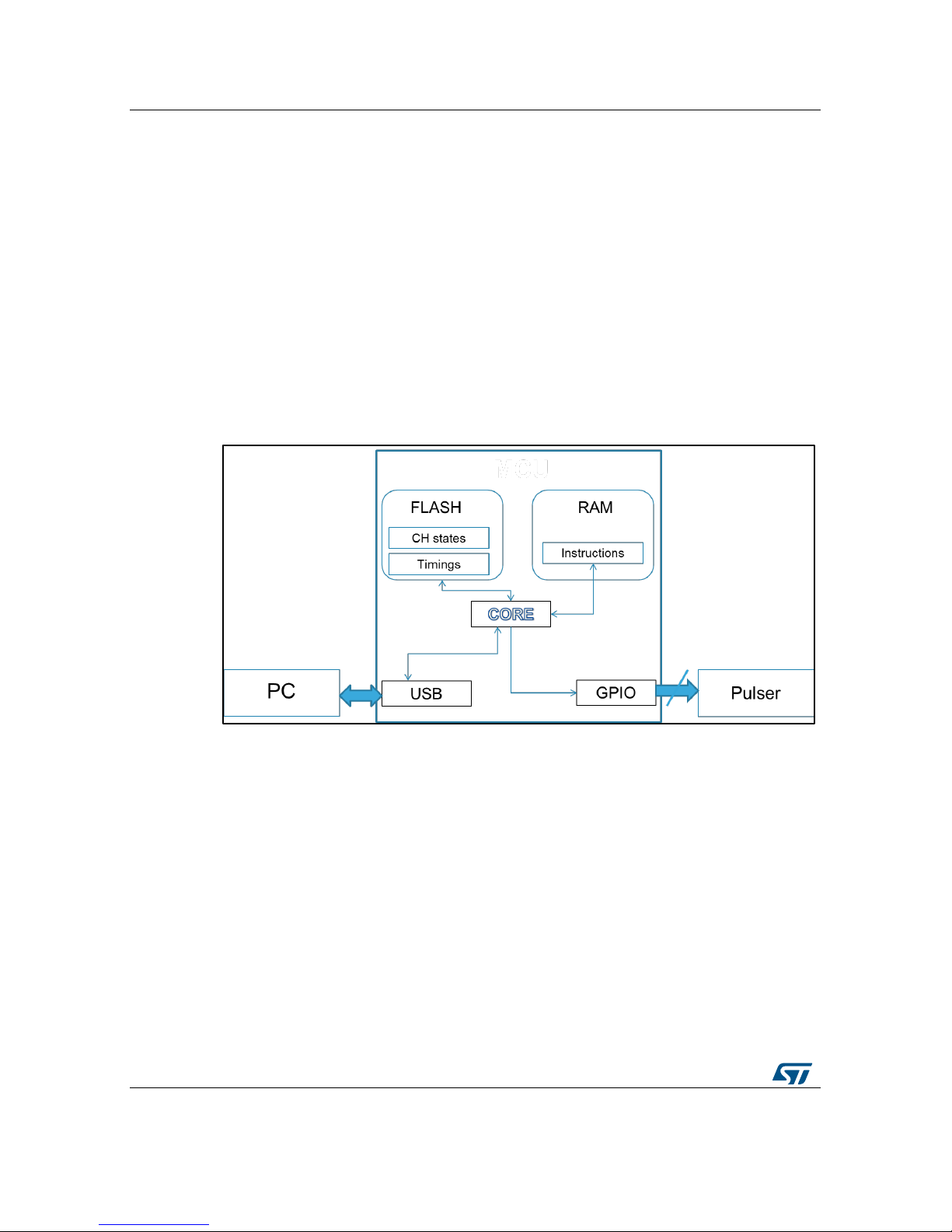
Figure 6: Solution 2 with direct MCU core intervention
3.3 Stored patterns
The STEVAL-IME011V2 can store four different patterns in the MCU Flash memory to
demonstrate the achievable performance at the pulser outputs.
Four selectable programs already stored in STM32 Flash memory form the default set
which is available and ready to use (flagged by L1 to L4 LEDs).
Program 1:
•XDCR_A: pulse wave mode, TX0 switching, 5 pulses, time-period TP = 400 ns and
PRF = 150 µs
•XDCR_B: pulse wave mode, TX0 switching, 5 pulses in counter phase respect to
XDCR_A, time-period TP = 400 ns and PRF = 150 µs
•XDCR_C: pulse wave mode, TX1 switching, 5 pulses, time-period TP = 200 ns and
PRF = 150 µs
•XDCR_D: pulse wave mode, TX1 switching, 5 pulses in counter phase with respect to
XDCR_C, time-period TP = 200 ns and PRF = 150 µs