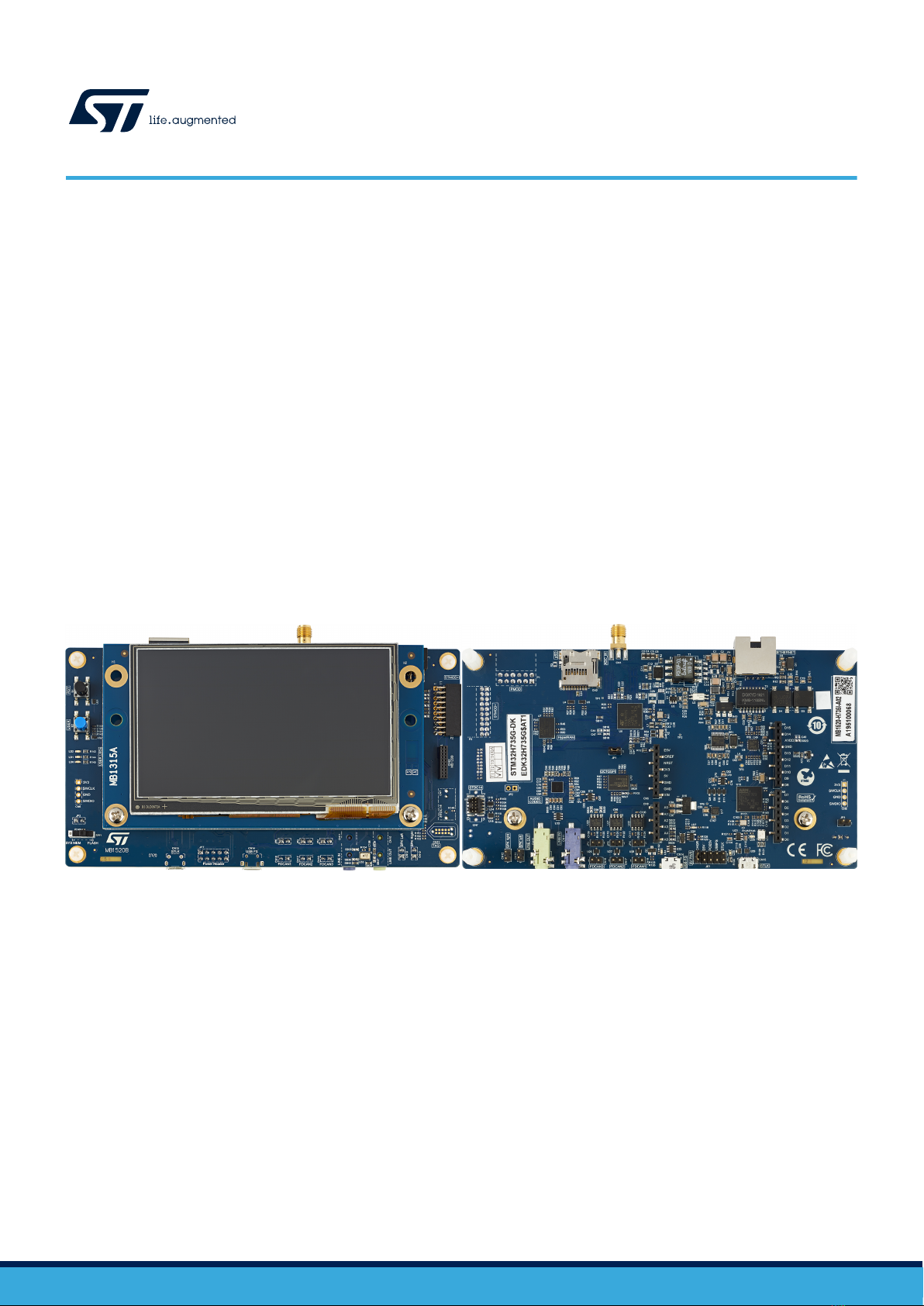
ST STM32H735G-DK User manual

Introduction
The STM32H735G-DK Discovery kit is designed as a complete demonstration and development platform for STMicroelectronics
Arm® Cortex®-M7 core-based STM32H735IG microcontroller. This microcontroller features five I²C, six SPIs with four
multiplexed full-duplex I2S interfaces, five USARTs, five UARTs and one ULP UART, one TT/CAN FD, two CAN FDs, two 16-bit
ADCs and one 12-bit ADC, two 12-bit DACs, two SAIs, two Octo-SPI interfaces with OTFDEC crypto, FMC interface, two
SDMMC controllers, two analog comparators, one SPDIF-RX, DFSDM (8 channels / 4 filters), one USB OTG HS and one USB
OTG FS, Ethernet MAC, DCMI interface, TFT LCD controller interface, JTAG and SWD for debugging support.
The STM32H735G-DK Discovery kit offers everything required by the user to get started quickly and develop applications easily.
The hardware features on the board help to evaluate the following peripherals: USB OTG FS, 10/100-Mbit Ethernet, microSD™,
USART, SAI audio codec stereo with two audio jacks for input/output, ST MEMS digital microphone, 128-Mbit HyperRAM™
memory, 512-Mbit Octo-SPI NOR Flash memory, CAN FD, 20-pin microphone MEMS connector with DFSDM interface, 4.3-inch
RGB TFT-LCD display with capacitive touch panel. The ARDUINO® Uno V3 compatible connectors, Pmod™, and STMod+
connectors allow easy connection of extension shields or daughterboard for specific applications.
The integrated STLINK-V3E provides an embedded in-circuit debugger and programmer for the STM32 MCU.
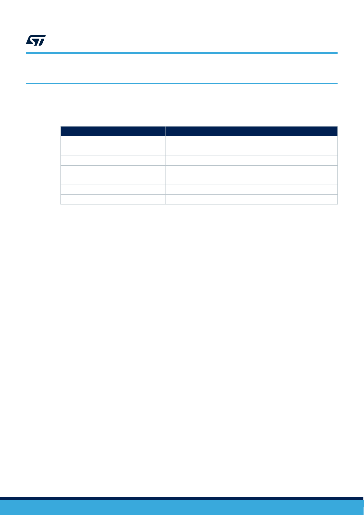
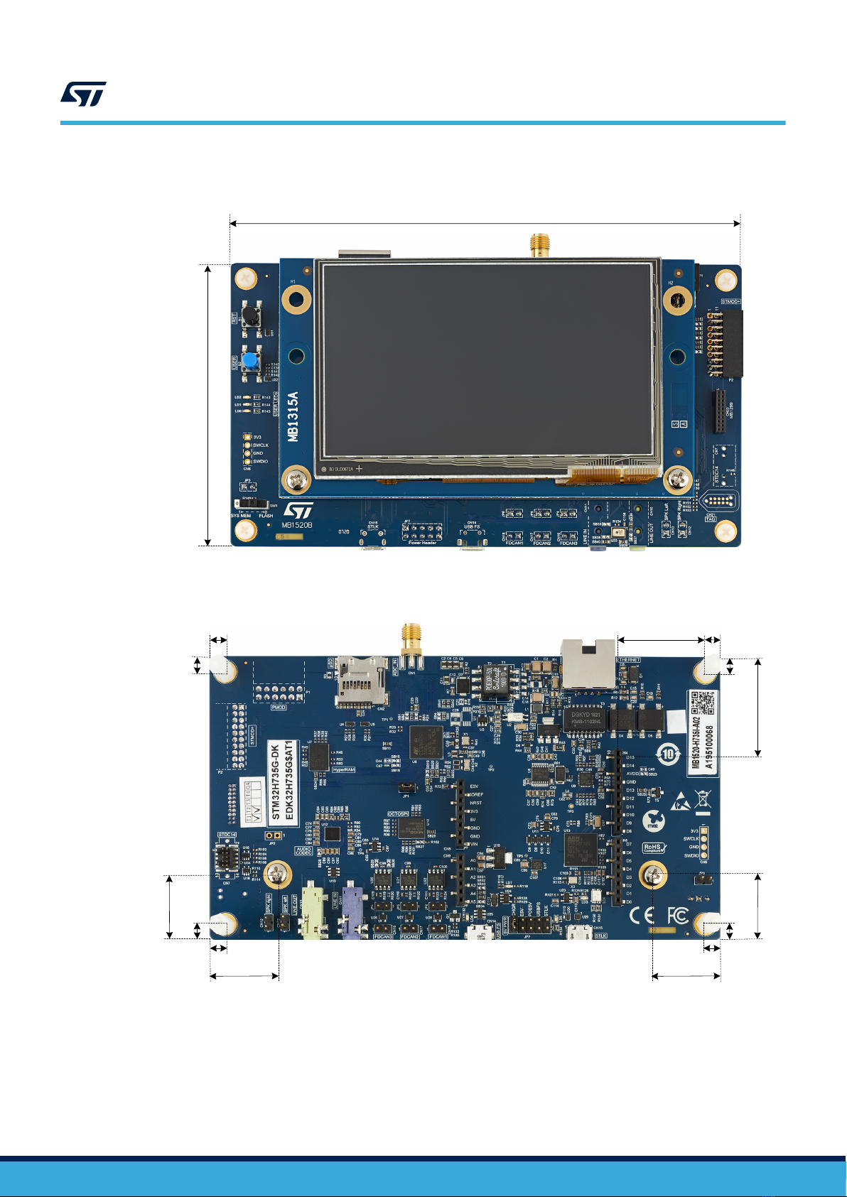
Figure 1. STM32H735G-DK Discovery kit (top view) Figure 2. STM32H735G-DK Discovery kit (bottom view)
Pictures are not contractual.
Discovery kit with STM32H735IG MCU
UM2679
User manual
UM2679 - Rev 1 - April 2020
For further information contact your local STMicroelectronics sales office. www.st.com

1Features
• STM32H735IGK6U microcontroller featuring 1 Mbyte of Flash memory and 564 Kbytes of SRAM in
UFBGA176+25 package
• 4.3" TFT 480×272 pixels colored LCD module with capacitive touch panel and RGB interface
• Ethernet compliant with IEEE-802.3-2002 and PoE (Power over Ethernet)
• USB OTG FS
• SAI audio codec
• One ST-MEMS digital microphone
• 512-Mbit Octal-SPI NOR Flash memory
•128-Mbit HyperRAM™
• Two user LEDs
• User and reset push-buttons
• Fan-out daughterboard
• Three CAN FDs
• Board connectors:
– USB FS Micro-AB
– USB ST-LINK Micro-B
– Ethernet RJ45
– Stereo headset jack including analog microphone input
– Audio header for external speakers
– microSD™ card
– TAG connector 10-pin footprint
– SMA connector
– Arm® Cortex® 10-pin 1.27 mm-pitch debug connector over STDC14 footprint
– ARDUINO® Uno V3 expansion connector
– STMod+ expansion connector
– Pmod™ Type-2A and Type-4A expansion connector
– Audio MEMS daughterboard expansion connector
• Flexible power-supply options:
– STLINK-V3E USB connector
– USB OTG FS connector
– 5 V delivered by RJ45 (Power over Ethernet)
– 5 V delivered by ARDUINO®
– USB charger
• On-board STLINK-V3E debugger/programmer with USB re-enumeration capability: mass storage, Virtual
COM port, and debug port
• Comprehensive free software libraries and examples available with the STM32CubeH7 MCU Package
• Support of a wide choice of Integrated Development Environments (IDEs) including IAR Embedded
Workbench®, MDK-ARM, and STM32CubeIDE
Note: Arm is a registered trademark of Arm Limited (or its subsidiaries) in the US and/or elsewhere.
UM2679
Features
UM2679 - Rev 1 page 2/42

2Ordering information
To order the STM32H735G-DK Discovery kit, refer to Table 1. Additional information is available from the
datasheet and reference manual of the target STM32.
Table 1. Ordering information
Order code Board references Target STM32
STM32H735G-DK
• MB1520
• MB1315(1)
• MB1280(2)
STM32H735IGK6U
1. LCD board.
2. Fan-out board.
2.1 Product marking
Evaluation tools marked as “ES” or “E” are not yet qualified and therefore not ready to be used as reference
design or in production. Any consequences deriving from such usage will not be at ST charge. In no event, ST will
be liable for any customer usage of these engineering sample tools as reference designs or in production.
“E” or “ES” marking examples of location:
• On the targeted STM32 that is soldered on the board (For an illustration of STM32 marking, refer to the
STM32 datasheet “Package information” paragraph at the www.st.com website).
• Next to the evaluation tool ordering part number that is stuck or silk-screen printed on the board.
This board features a specific STM32 device version, which allows the operation of any bundled commercial
stack/library available. This STM32 device shows a "U" marking option at the end of the standard part number
and is not available for sales.
In order to use the same commercial stack in his application, a developer may need to purchase a part number
specific to this stack/library. The price of those part numbers includes the stack/library royalties.
2.2 Codification
The meaning of the codification is explained in Table 2. The order code is mentioned on a sticker placed on the
top or bottom side of the board.
Table 2. Codification explanation
STM32TTXXY-DK Description Example: STM32H735G-DK
STM32TT MCU series in STM32 32-bit Arm Cortex MCUs STM32H7 Series
XX MCU product line in the series STM32H725/735
YSTM32 Flash memory size:
• G for 1 Mbyte 1 Mbyte
DK DK for Discovery kit Discovery kit
UM2679
Ordering information
UM2679 - Rev 1 page 3/42

3Development environment
The STM32H735G-DK Discovery kit runs with the STM32H735IG 32-bit microcontroller based on the Arm®
Cortex®-M7 core.
3.1 System requirements
• Windows® OS (7, 8 and 10), Linux® 64-bit, or macOS®
• USB Type-A to Micro-B cable
Note: macOS® is a trademark of Apple Inc. registered in the U.S. and other countries.
All other trademarks are the property of their respective owners.
3.2 Development toolchains
• IAR Systems - IAR Embedded Workbench®(1)
• Keil® - MDK-ARM(1)
• STMicroelectronics - STM32CubeIDE
1. On Windows® only.
3.3 Demonstration software
The demonstration software, included in the STM32Cube MCU Package corresponding to the on-board
microcontroller, is preloaded in the STM32 Flash memory for easy demonstration of the device peripherals in
standalone mode. The latest versions of the demonstration source code and associated documentation can be
downloaded from www.st.com.
UM2679
Development environment
UM2679 - Rev 1 page 4/42

4Conventions
Table 3 provides the conventions used for the ON and OFF settings in the present document.
Table 3. ON/OFF convention
Convention Definition
Jumper JPx ON Jumper fitted
Jumper JPx OFF Jumper not fitted
Jumper JPx [1-2] Jumper fitted between Pin 1 and Pin 2
Solder bridge SBx ON SBx connections closed by 0 Ω resistor
Solder bridge SBx OFF SBx connections left open
Resistor Rx ON Resistor soldered
Resistor Rx OFF Resistor not soldered
UM2679
Conventions
UM2679 - Rev 1 page 5/42

5Delivery recommendations
Before the first use, make sure that no damage occurred to the board during shipment and no socketed
components are not firmly fixed in their sockets or loose in the plastic bag.
In particular, pay attention to the following component:
• TFT display MB1315 daughterboard in the CN19 connector.
For product information related to the STM32H735IGK6U microcontroller, visit the www.st.com website.
UM2679
Delivery recommendations
UM2679 - Rev 1 page 6/42

6Hardware layout and configuration
The STM32H735G-DK Discovery kit is designed around the STM32H735IGK6U target microcontroller, packaged
in TFBGA176+25. The hardware block diagram (Refer to Figure 3) illustrates the connections between the
STM32H735IGK6U microcontroller and the peripheral components. Figure 4 and Figure 5 help to locate these
features on the STM32H735G-DK Discovery kit. Figure 6 and Figure 7 give the mechanical dimensions of the
STM32H735G-DK board.
Figure 3. Hardware block diagram
GPIO
OCTOSPI2128-Mbit HyperRAMTM
SWD
4.3-inch RGB LCD
OCTOSPI1 Audio codec and
amplifier
microSDTM connector
PWR supply
SDIO1
PWR
UART7
USART3
LCD
DFSDM1
RTC / HSE
PDM
SAI1
STLINK-V3E
32.768 kHz crystal /
25 MHz oscillator
512-Mbit Octo-SPI Flash
Tag connector
SWD connector
USB connector
Audio connector
(5 MEMS microphones)
User LEDs
OTG FS
STM32H735IG
TFBGA176+25
Stereo jack (IN/OUT)
RMII
PoE (Power over
Ethernet)
Ethernet
I2C4
ARDUINO® connector
STMod+ connector
PmodTM connector
SPI5
UART1
CAN FD1/2/3 3x CAN FDsSAI4
MEMS microphone
(on-board)
UM2679
Hardware layout and configuration
UM2679 - Rev 1 page 7/42

Figure 4. STM32H735G-DK board layout (top view)
CN19: LCD connector
P1: PmodTM connector
P2: STMod+ connector
CN20: Audio connector
CN21: Tag connector
B1: Reset button
SW1: Switch
B2: User button
LD1/LD2: User LEDs
U33: Digital microphone
LD8: ARDUINO® LED
Figure 5. STM32H735G-DK board layout (bottom view)
CN3:
Ethernet
connector
CN6: DFU connector
U13: MCU STLINK-V3E
LD5: 5V Power LED
CN14: USB
OTG FS
connector
U6:
STM32H735IGK6U
U7:
HyperRAMTM
CN12:
Right speaker
connector
CN16/17/18:
CAN-FD
connectors
CN10:
Line-out
connector
CN11:
Line-in
connector
JP7:
Power
selector
CN15: USB
ST-LINK
connector
LD6: ST-LINK COM LED
CN1:
ADC_IN
connector
CN2:
microSDTM
connector
U10: Octo-SPI Flash
CN7: MIPI-10 connector
CN13:
Left speaker
connector
UM2679
Hardware layout and configuration
UM2679 - Rev 1 page 8/42

Figure 6. STM32H735G-DK mechanical dimensions (top view) in millimeters
159.00
88.00
Figure 7. STM32H735G-DK mechanical dimensions (bottom view) in millimeters
5.00
5.0033.005.00
5.00
21.25
5.00
20.20
21.25
5.00
5.00
20.20 31.30
5.00
UM2679
Hardware layout and configuration
UM2679 - Rev 1 page 9/42

6.1 Embedded STLINK-V3E
6.1.1 Description
There are two different ways to program and debug the onboard STM32 MCU:
• Using the embedded STLINK-V3E
• Using an external debug tool connected to CN7 MIPI-10 connector
The STLINK-V3E programming and debugging tool is integrated into the STM32H735G-DK Discovery kit.
The embedded STLINK-V3E supports only SWD and VCP for STM32 devices. For information about debugging
and programming features, refer to the technical note Overview of ST-LINK derivatives (TN1235), which describes
in detail all the STLINK-V3E features.
Features supported in STLINK-V3E:
• 5 V power supplied by the CN15 USB connector
• USB 2.0 high-speed-compatible interface
• JTAG and serial wire debugging (SWD) specific features:
– 3 V to 3.6 V application voltage on the JTAG/SWD interface and 5V tolerant inputs
– JTAG
– SWD and serial viewer (SWV) communication
• Direct firmware update feature (DFU) (CN6)
• STDC14 (MIPI10) compatible connector (CN7)
• LD6 status LED (COM) which blinks during communication with the PC
• LD3 fault red LED (OC) alerting on USB overcurrent request
• 5 V / 500 mA output power supply capability (U23) with current limitation and LED
• LD5 5 V power green LED (5V)
6.1.2 Drivers
Before connecting the STM32H735G-DK board to a Windows® PC via USB, the user must install a driver for the
STLINK-V3E (not required for Windows 10®). It is available on the www.st.com website.
In case the STM32H735G-DK board is connected to the PC before the driver is installed, some STM32H735G-DK
interfaces may be declared as “Unknown” in the PC device manager. In this case, the user must install the
dedicated driver files, and update the driver of the connected device from the device manager as shown in
Figure 8.
Note: Prefer using the USB Composite Device handle for a full recovery.
Figure 8. USB composite device
Note: 37xx:
• 374E for STLINK-V3E without bridges functions
• 374F for STLINK-V3E with bridges functions
UM2679
Embedded STLINK-V3E
UM2679 - Rev 1 page 10/42

6.1.3 STLINK-V3E firmware upgrade
The STLINK-V3E embeds a firmware upgrade mechanism for in-situ upgrades through the USB port. As the
firmware may evolve during the lifetime of the STLINK-V3E product (for example new functionalities, bug fixes,
support for new microcontroller families), it is recommended to visit the www.st.com website before starting to use
the STM32H735G-DK Discovery kit and periodically, to stay up-to-date with the latest firmware version.
6.1.4 Using an external debug tool to program and debug the on-board STM32
There are 2 basic ways to support an external debug tool:
1. Keep the embedded STLINK-V3E running. Power on the STLINK-V3E at first until the COM LED lights RED.
Then connect the external debug tool through CN7 MIPI-10 debug connector.
2. Set the embedded STLINK-V3E in a high-impedance state. When setting the jumper JP3 (STLK_RST) ON,
the embedded STLINK-V3E is in RESET state and all GPIOs are in high impedance. Then the user can
connect his external debug tool on the debug connector CN7.
Figure 9. Connecting an external debug tool to program the on-board STM32
JP3: STLK_RST
CN7: External debug tool connector
JP7: Power supply selection
CN15: ST-LINK USB connector
Table 4 describes the CN7 MIPI10 debug connector pinout.
Table 4. CN7 MIPI-10 debug connector pinout
MIPI-10 pin STDC14 pin CN7 Designation
- 1 NC Reserved
- 2 NC Reserved
1 3 T_VCC Target VCC
2 4 T_SWDIO Target SWDIO using SWD protocol or Target JTMS (T_JTMS) using JTAG
protocol
3 5 GND Ground
4 6 T_SWCLK Target SWCLK using SWD protocol or Target JCLK (T_JCLK) using JTAG
protocol
5 7 GND Ground
6 8 T_SWO Target SWO using SWD protocol or Target JTDO (T_JTMS) using JTAG
protocol
UM2679
Embedded STLINK-V3E
UM2679 - Rev 1 page 11/42

MIPI-10 pin STDC14 pin CN7 Designation
7 9 T_JRCLK Not used by SWD protocol, Target JRCLK (T_JRCLK) using JTAG protocol,
only for specific use
8 10 T_JTDI Not used by SWD protocol, Target JTDI (T_JTDI) using JTAG protocol, only
for external tools
9 11 GNDDetect GND detect for plug indicator, used on SWD and JTAG neither
10 12 T_NRST Target NRST using SWD protocol or Target JTMS (T_JTMS) using JTAG
protocol
- 13 T_VCP_RX Target RX used for VCP (must be UART dedicated to Bootloader)
- 14 T_VCP_TX Target TX used for VCP (must be UART dedicated to Bootloader)
6.2 Power supply
The STM32H735G-DK Discovery kit is designed to be powered by a 5 V DC power source. One of the following
five inputs can be used, upon appropriate board configuration:
1. Micro-B USB receptacle CN15 of STLINK-V3E without enumeration: up to 500 mA can be supplied to the
board (JP7 jumper setting on ‘CHGR’ position on the silkscreen)
2. Micro-B USB receptacle CN15 of STLINK-V3E with enumeration feature (see Supplying the board through
the STLINK-V3E USB port), up to 500 mA can be supplied to the board (JP7 jumper setting ’STLK’ position
on the silkscreen)
3. An external 7 to 12V power supply from CN5 pin 8: name VIN on the silkscreen, extension connectors for
ARDUINO® Uno shields or daughterboard (JP7 jumper setting on ‘E5V’ on the silkscreen).
4. 48V DC power from RJ45 connector CN3 (Ethernet): In this case, the on-board module POE (Power Over
Ethernet) generates the 5 V supply voltage with up to 600 mA. This module is a powered device complying
with IEEE 802.3af, class ½ standard. The external power supply must be fully IEEE 802.3af compliant (JP7
jumper setting on ‘POE5V’ on the silkscreen).
5. Micro-AB USB receptacle CN14 of the USB_OTG_FS interface: marked USB OTG FS on the board. (JP7
jumper setting on ‘USBFS’ on the silkscreen).
The LD5 green LED turns ON when the voltage on the power line marked 5V is present. All supply lines required
for the operation of the STM32H735G-DK components are derived from this 5V line.
Note: The Discovery board must be powered by a power supply unit or by auxiliary equipment complying with the
standard EN-60950-1: 2006+A11/2009, and must be Safety Extra Low Voltage (SELV) with limited power
capability.
6.2.1 Supplying the board through the STLINK-V3E USB port: 5 V/500 mA
To power the STM32H735G-DK in this way, the USB host (a PC) gets connected to the Micro-B USB receptacle
of the board via a USB cable. The connection event starts with the USB enumeration procedure. In its initial
phase, the host USB port current supply capability is limited to 100 mA. This is sufficient since only the STLINK-
V3E part of the STM32H735G-DK draws power at that time: The U23 STMPS2151 power switch is set to the OFF
position, which isolates the rest of the board from the power source.
In the next phase of the enumeration procedure, the host PC informs the STLINK-V3E that it is able to supply
current up to 300 mA. If the answer is positive, the STLINK-V3E sets the U23 STMPS2151 switch to the ON
position to supply power to the rest of the board. Otherwise, CN5 pin8 (VIN) can be used to supply the board
instead. If a short-circuit occurs on the board, the STMPS2151 power switch protects the USB port of the host PC
against a current demand exceeding 500 mA. In such an event, the LD3 LED lights up.
The STM32H735G-DK board can also be supplied from a USB power source that does not support enumeration,
such as a USB charger. In this case, the STLINK-V3E bypasses STMPS2151 power regardless of the
enumeration procedure result and passes the power unconditionally to the board. The LD5 green LED turns ON
whenever the whole board is powered.
6.2.2 Supplying the board from VIN: 7 V to 12 V/800 mA
It may happen that the STM32H735G-DK board requires a supply current higher than 500 mA. In such a case,
the board can be supplied through pin8 (marked ‘VIN’ on the board) of the CN5 ARDUINO® connector.
UM2679
Power supply
UM2679 - Rev 1 page 12/42

Note that using STLINK-V3E for debugging when powering the board with an external power supply, it is
important to power the board before connecting the host PC to CN15. This requires the following sequence to be
respected:
1. Set the jumper JP7 “E5V” [7-8].
2. Connect the external power source to the pin 8 of CN5.
3. Check that the green LED LD5 is turned ON.
4. Connect the host PC to USB connector CN15.
If this order is not respected, the board may be powered by VBUS first from STLINK-V3E, and the following risks
may be encountered:
1. If more than 500 mA current is needed by the board, the PC may be damaged or current can be limited by
the PC. As a consequence, the board is not powered correctly.
2. 500 mA is requested at the enumeration step, so there is a risk that the request is rejected and enumeration
does not succeed if the PC cannot provide such current.
Table 5. External power sources: VIN from 7 to 12V
Input power
name
Connector
pins
Voltage
range Max current Limitation
VIN CN5 pin 8 From 7 V to
12 V 800 mA
From 7 to 12 V only and input current capability is linked to
input voltage:
• 800 mA input current when VIN = 7 V
• 450 mA input current when 7 V < VIN < 9 V
• 250 mA input current when 9 V < VIN < 12 V
6.2.3 Supplying the board with an external USB charger: 5 V
When the STM32H735G-DK board is powered by an external USB charger through CN15, refer to Table 6, the
jumper must be placed on pin 9-10 of JP7 (“CHGR” on the silkscreen). Note that in this power supply mode, the
debug features are not available.
Table 6. External power source: 5V_USB_CHGR
Input power name Connector pins Voltage range Max current
5V_USB_CHGR CN15 5 V -
6.2.4 MCU power supply - SMPS or LDO configurations
There are three possible solutions to provide power to the MCU VCORE logic supply: SMPS, LDO, and SMPS with
LDO. Power consumption in Run mode is significantly improved by generating VCORE from the internal DC/DC
converter (SMPS). The default power supply for VCORE logic must be SMPS. Some hardware modifications are
required to switch to LDO or SMPS with LDO configurations. The hardware modifications are listed below:
•SMPS mode (default):
– SB2, SB13, SB20, SB21, and L3: ON
– SB1, SB3, SB16, SB18, and SB19: OFF
•LDO mode:
– SB1, SB3, and SB19: ON
– SB2, SB16, SB18, SB20, SB21, and L3: OFF
•SMPS with LDO mode:
– SB3, SB13, SB19, SB21, and L3: ON
– SB1, SB2, SB16, SB1, and SB20: OFF
Caution:
If the board SMPS/LDO firmware PWR configuration does not match its hardware configuration, a deadlock
occurs. After the reset, the ST-LINK cannot connect to the target anymore.
UM2679
Power supply
UM2679 - Rev 1 page 13/42

The firmware PWR configuration must be set as follows in function SystemClock_Config in file main.c:
• If the hardware configuration is Direct SMPS (Default configuration):
HAL_PWREx_ConfigSupply(PWR_DIRECT_SMPS_SUPPLY);
• If the hardware configuration is LDO:
HAL_PWREx_ConfigSupply(PWR_LDO_SUPPLY);
If a deadlock occurs because of a mismatch between hardware and firmware PWR settings (SMPS/LDO), the
user can recover the board by applying the following procedure:
1. Power off the board.
2. Set SW1 (BOOT0) to 1 (system memory). This changes the BOOT0 pin to 1 instead of 0, thus changing the
device boot address to boot address 1 and making the bootloader start in System memory. This avoids
starting firmware in the user Flash with a wrong SMPS/LDO configuration versus the hardware board
configuration.
3. Power on the board and connect using STM32CubeProgrammer (STM32CubeProg).
4. Erase the user Flash.
5. Power off the board and set SW1 to 0.
6. The board is recovered and can be used normally with matching firmware PWR.
Table 7. Internal SMPS, LDO and board configuration
(1)
Config1
LDO ON
(SMPS OFF)
Config2
SMPS ON
(LDO OFF)
(Default config)
Config3
(SMPS and LDO cascaded)
SMPS ON
LDO ON
SB1 ON OFF OFF
SB2 OFF ON OFF
SB3 ON OFF ON
SB13 ON ON ON
SB16 OFF OFF OFF
SB18 OFF OFF OFF
SB19 ON OFF ON
SB20 OFF ON OFF
SB21 OFF ON ON
L3 OFF ON ON
1. The default setting is in bold.
6.3 MCU current-consumption measurement
The JP1 jumper allows the current consumption of STM32H735IGK6U to be measured directly by removing the
jumper and replacing it with an external ammeter. If there is no ammeter, STM32H735IGK6U is not powered.
6.4 Clock source
Three clock sources are available on the STM32H735G-DK board, as described below:
• X1 25 MHz oscillator for the STM32H735IGK6U HSE system clock and Ethernet PHY
• X2 32.768 kHz crystal for the STM32H735IGK6U embedded RTC
• X3 25 MHz oscillator for the STLINK-V3E
UM2679
MCU current-consumption measurement
UM2679 - Rev 1 page 14/42

6.5 Reset sources
The general reset of the STM32H735G-DK board is active LOW. The reset sources include:
• B1 Reset button
• Embedded STLINK-V3E
• ARDUINO® Uno shield board through CN5 connector (pin 3)
• STDC14 receiver
• TAG connector
The general reset is connected to following Peripheral reset function:
• Octo-SPI Flash memory reset
• LCD reset (Option not connected by default)
•HyperRAM™ memory
• Ethernet
UM2679
Reset sources
UM2679 - Rev 1 page 15/42

7Board functions
7.1 TFT color LCD 480x272 pixels
The STM32H735G-DK board includes a 4.3-inch 480x272 LCD-TFT board (MB1315), which is connected to the
RGB interface of the STM32H735IGK6U through a 50-pin connector (CN19). The MB1315 LCD board uses the
RK043FN48H-CT672B TFT-LCD from Rocktech with the driving system, white LED backlight, and capacitive
touch panel. The touchscreen controller interfaces with the STM32H735IGK6U via the bidirectional I2C4 bus,
since the TFT LCD reset is controlled by PH6 GPIO (LCD_RST signal) by default (SB43 ON and SB44 OFF). The
possibility to control the LCD reset by the general reset (NRST) is also available on the STM32H735G-DK board.
In this case, SB44 must be ON and SB43 OFF.
7.2 USB OTG FS
The STM32H735G-DK board supports USB OTG full-speed communications via the CN14 USB Micro-AB
connector. The USB connector can power the STM32H735G-DK board with a 5V DC supply voltage, at a current
up to 500 mA. A USB power switch is also connected to VBUS and provides power to CN14. The green LED LD4
is lit when one of the following events occurs:
• The power switch is ON and STM32H735G-DK operates as a USB host.
• VBUS is powered by another USB host when the STM32H735G-DK board works as a USB device.
The red LED LD7 is lit when an overcurrent occurs (Current higher than 500 mA).
Note: The STM32H735G-DK board must be powered by an external power supply when using the OTG function.
7.3 Ethernet
The STM32H735G-DK board supports 10/100-Mbit Ethernet communication with a MICROCHIP LAN8742A-CZ-
TR PHY and integrates an RJ45 connector CN3. The Ethernet PHY is connected to the STM32H735IGK6U
microcontroller via an RMII interface.
The PHY 25 MHz clock is generated from the X1 oscillator, while the PHY RMII_REF_CLK generates the 50 MHz
clock for the STM32H735IGK6U.
7.4 Power over Ethernet
The STM32H735G-DK board integrates a power module that uses Ethernet. This module is an IEEE802.3af
compliant, class 1 / 2 PoE converter based on the simple diode rectified Flyback topology around the PM88800A
component from ST. This module “Powered Device” accepts an input voltage of 48 V and is able to provide 5 V
with 600 mA.
7.5 microSD™ card
A slot (CN2) for microSD™ card (SD 2.0 compliant) is available on the STM32H735G-DK board and is connected
to the SDOI1 interface of the STM32H735IGK6U. The microSD™ card detection is managed by the uSD_Detect
signal (PF5). When a microSD™ card is inserted in the slot, the uSD_Detect signal level is LOW, otherwise, it is
HIGH.
7.6 Audio
An audio codec WM8994ECS/R from CIRRUS with four DACs and two ADCs is connected to the
STM32H735IGK6U SAI1 interface.
It communicates with the STM32H735IGK6U microcontrollers via an I²C-bus shared with the touch panel of the
RGB LCD and the STMod+ connector. The I²C-bus address of the WM8994ECS/R coded is 0011010.
UM2679
Board functions
UM2679 - Rev 1 page 16/42

Several audio connections are available on the on STM32H735G-DK board:
• The analog input line is connected to the WM8994ECS/R ADC through the blue audio jack (CN11).
• The analog output line is connected to the WM8994ECS/R DAC via the green audio jack (CN10).
• Two external speakers can be connected to the WM8994ECS/R via CN13 for the left speaker and CN12 for
the right speaker. The STM32H735G-DK board features one digital MP34DT05-A microphone (ST-MEMS
microphone). It is connected to the input digital microphone of the STM32H735IGK6Uand is managed by the
PDM functionality.
Limitation:
On the STM32H735G-DK board, SAI1 signals are sharing the same I/Os with SPI5 and UART7 signals. As a
consequence, when using SAI1 interface for the audio codec, the user must make sure that there is nothing
connected on STMod+ (1,2,3,4 pins), Pmod™ (1,2,3,4 pins) and ARDUINO® (D10, D11, D12, D13 pins)
connectors.
DIGITAL microphone
The U33 on the STM32H735G-DK board is STMicroelectronics MP34DT05-A MEMS digital omnidirectional
microphone providing PDM (pulse density modulation) output. The microphone is supplied with a programmable
clock generated directly by the STM32H735IGK6U (SAI4_CK2 signal) or the audio codec (DMICCLK signal).
As an option, the microphone can be connected to U12 (Wolfson WM8994 audio codec device). In that
configuration, WM8994 also supplies the PDM clock to the microphone. Regardless of the microphone routing
(STM32H735IGK6U or WM8994 codec), the power can be supplied either by the 3V3 or the MICBIAS1 output of
the WM8994 codec device.
Table 8 shows the settings of all solder bridges associated with the digital microphone on the board.
Table 8. Digital microphone – Solder bridge configuration
Solder bridge Setting(1) Configuration
SB40, SB39
SB38, SB28
SB40, SB39 OFF
SB38, SB28 ON
The PDM clock for the digital microphone is provided by the WM8994
codec.
SB40, SB39 ON
SB38, SB28 OFF
The PDM clock for the digital microphone is provided by the
STM32H735IGK6U MCU
SB36, SB37
SB36 OFF
SB37 ON
The power supply of the digital microphone is generated by the
WM8994 codec (MICBIAS1).
SB36 ON
SB37 OFF The power supply of the digital microphone is 3V3
1. The default setting is in bold.
7.7 CAN FD
The STM32H735G-DK board supports three channels of CAN FD (Flexible data-rate CAN) compliant bus based
on 3V3 CAN transceiver.
Limitation:
On the STM32H735G-DK board, the CAN‑FD3 signals are sharing with SPI5 and UART7 signals. As a
consequence, when using CAN‑FD3 interface, the user must make sure that there is nothing connected on
STMod++ (1,2,3,4 pins), Pmod™ (1,2,3,4 pins) and ARDUINO® (D10, D11, D12, D13 pins) connectors.
UM2679
CAN FD
UM2679 - Rev 1 page 17/42

Table 9. CAN‑FD3 - Solder bridge configuration
Solder bridge Setting(1) Configuration
SB29, SB30
SB29, SB30 ON TXD and RXD of MCD2562FD are connected to PF7 (FDCAN3_TX)
and PF6 (FDCAN3_RX) of STM32H735IGK6U MCU.
SB29, SB30 OFF
(CAN‑FD3 bus not connected)
TXD and RXD of MCD2562FD are disconnected to PF7
(FDCAN3_TX) and PF6 (FDCAN3_RX) of STM32H735IGK6U MCU.
1. The default setting is in bold.
7.8 Octo-SPI NOR Flash memory
The STM32H735G-DK board includes a 512-Mbit Octo-SPI NOR Flash memory device (MX25LM51245GXDI00
from MACRONIX), which is connected to the OCTOSPI1 interface of the STM32H735IGK6U microcontroller.
MX25LM51245GXDI00 operates in a single transfer rate (STR) or double transfer rate (DTR) mode.
The RESETn of the Flash memory is connected to the general reset (NRST) of the STM32H735G-DK board.
7.9 HyperRAM™ memory
The STM32H735G-DK board adds an external 128-Mbit HyperRAM™ (S70KL1281DABHI023 from Cypress) that
is connected to the STM32H735IGK6U via the OCTOSPI2 interface.
7.10 Virtual COM port
The serial interface USART3 (PD8/PD9) that supports the bootloader is directly available as a Virtual COM port of
the PC connected to STLINK-V3E USB connector CN15. The VCP configuration is the following:
• 115200 bps
• 8-bit data
• No parity
• One-stop bit
• No flow control
7.11 TAG
One TAG interface footprint (CN21) is reserved on the STM32H735G-DK board, which can be used for the board
debugging and programming.
7.12 Buttons and LEDs
The black button (B1) located on the top side is the reset of the STM32H735IGK6U microcontroller.
The blue button (B2) located on the top side is to be used as a digital input or as a wakeup-alternate function.
When the button is depressed the logic state is LOW, otherwise, the logic state is HIGH.
UM2679
Octo-SPI NOR Flash memory
UM2679 - Rev 1 page 18/42

Two LEDs located on the top side, the red LD2 and the green LD1 (refer to Figure 4), are available for the user.
To light a LED, a low-logic state HIGH must be written in the corresponding GPIO register. Table 10 shows the
assignment of the control ports to the LED indicators.
Table 10. Button and LED control port
Reference Color Name Comment
B1 BLACK RESET -
B2 BLUE USER Wake-up alternate function
LD7 RED USB_FS_OVCR PG13
LD6 BICOLOR (RED/GREEN) STLINK-V3E COM Green when communication ongoing
LD3 RED STLINK-V3E Over Current -
LD4 GREEN VBUS USB FS PA9
LD5 GREEN POWER 5V power supply available
LD2 RED USER2 PC2
LD1 GREEN USER1 PC3
LD8 GREEN ARDUINO PF7
UM2679
Buttons and LEDs
UM2679 - Rev 1 page 19/42

8Board connectors
8.1 CN15 STLINK-V3E USB Micro-B connector
The CN15 USB connector is used to connect the embedded STLINK-V3E to the PC for programming and
debugging purposes.
Figure 10. CN15 Micro-B connector (Front view)
The related pinout for the USB ST-LINK connector is listed in Table 11.
Table 11. CN15 USB Micro-B connector pinout
Connector Pin number Pin name Signal name ST-LINK MCU pin Function
CN15
1 VBUS 5V_USB_CHARGER - 5 V power
2 DM USB_DEV_HS_CN_N PB14 USB differential pair M
3 DP USB_DEV_HS_CN_P PB15 USB differential pair P
4 ID - - -
5 GND - - GND
8.2 CN14 USB OTG FS Micro-AB connector
A USB OTG full-speed communication link is available at CN14 USB Micro-AB receptacle connector. Micro-AB
receptacle enables USB Host and USB Device features.
Figure 11. CN14 USB OTG FS Micro-AB connector (Front view)
UM2679
Board connectors
UM2679 - Rev 1 page 20/42
Table of contents
Other ST Motherboard manuals
Popular Motherboard manuals by other brands

Silicon Laboratories
Silicon Laboratories Si1102EK user guide

AXIOMTEK
AXIOMTEK EP600 Series user manual

Advantech
Advantech AIMB-232 Startup manual

WinSystems
WinSystems EBC-BX Operation manual

ASROCK
ASROCK ALIVENF5-ESATA2 PLUS - V1.0 installation guide

Avalue Technology
Avalue Technology EMX-Q170KP-B1R user manual