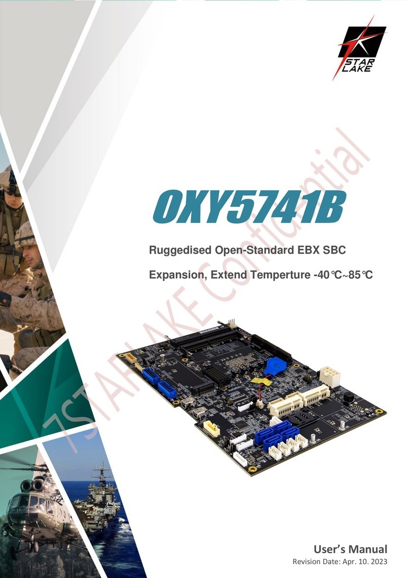
Star Lake OXY5363A User manual

User’s Manual
Revision Date: Feb.14.2022
OXY5363A
3.5" SBC Form Factor Intel®Apollo Lake Processor

OXY5323A User’s Manual
Revision Date: Feb.14.2022
1
Safety Information
Electrical safety
To prevent electrical shock hazard, disconnect the power cable from the electrical
outlet before relocating the system.
When adding or removing devices to or from the system, ensure that the power cables
for the devices are unplugged before the signal cables are connected. If possible,
disconnect all power cables from the existing system before you add a device.
Before connecting or removing signal cables from the motherboard, ensure that all
power cables are unplugged.
Seek professional assistance before using an adapter or extension cord. These
devices could interrupt the grounding circuit.
Make sure that your power supply is set to the correct voltage in your area.
If you are not sure about the voltage of the electrical outlet you are using, contact your
local power company.
If the power supply is broken, do not try to fix it by yourself. Contact a qualified service
technician or your local distributor.
Operation safety
Before installing the motherboard and adding devices on it, carefully read all the
manuals that came with the package.
Before using the product, make sure all cables are correctly connected and the power
cables are not damaged. If you detect any damage, contact your dealer immediately.
To avoid short circuits, keep paper clips, screws, and staples away from connectors,
slots, sockets and circuitry.
Avoid dust, humidity, and temperature extremes. Do not place the product in any area
where it may become wet.
Place the product on a stable surface.
If you encounter any technical problems with the product, contact your local distributor
Statement
All rights reserved. No part of this publication may be reproduced in any form or by
any means, without prior written permission from the publisher.
All trademarks are the properties of the respective owners.
All product specifications are subject to change without prior notice.

OXY5323A User’s Manual
Revision Date: Feb.14.2022
2
Revision History
Revision
Date (yyyy/mm/dd)
Changes
V1.0
2021/09/08
First release
V1.1
2022/02/14
Add Standard Compliance
Packing List
Item
Description
Q’ty
1
OXY5323A IEC-61850-3, IEEE-1613 1U Computer
1
2
Driver CD+ User’s manual
1
If any of the above items is damaged or missing, please contact your local
distributor.
Ordering information
Model
Description
OXY5323A-01ET
Intel®Apollo Lake-I E3930,DDR3L 1866MHz,1 x 204-pin SO-DIMM, Max. 8GB
(Non-ECC),2 x Intel® I210-IT Giga LAN,4 x USB 3.0,1 x HDMI 1.4, 1 x VGA,2 x
RJ-45,Normal Temperature: -20 to 70°C
OXY5323A-01UT
Intel®Apollo Lake-I E3930,DDR3L 1866MHz,1 x 204-pin SO-DIMM, Max. 8GB
(Non-ECC),2 x Intel® I210-IT Giga LAN,4 x USB 3.0,1 x HDMI 1.4, 1 x VGA,2 x
RJ-45,Wide Temperature (Optional*) : -40 to 85°C
OXY5323A-02ET
Intel®Apollo Lake-M N3350,DDR3L 1866MHz,1 x 204-pin SO-DIMM, Max. 8GB
(Non-ECC),2 x Intel® I210- IT Giga LAN,4 x USB 3.0,1 x HDMI 1.4, 1 x VGA,2 x
RJ-45,Normal Temperature: -20 to 70°C
OXY5323A-02UT
Intel®Apollo Lake-M N3350,DDR3L 1866MHz, x 204-pin SO-DIMM, Max. 8GB
(Non-ECC),2 x Intel® I210- IT Giga LAN,4 x USB 3.0,1 x HDMI 1.4, 1 x VGA,2 x
RJ-45, Wide Temperature (Optional*):-40 to 85°C
OXY5323A-03ET
Intel®Apollo Lake-M N4200,DDR3L 1866MHz,1 x 204-pin SO-DIMM, Max. 8GB
(Non-ECC),2 x Intel® I210- IT Giga LAN,4 x USB 3.0,1 x HDMI 1.4, 1 x VGA,2 x
RJ-45,Normal Temperature: -20 to 70°C
OXY5323A-03UT
Intel®Apollo Lake-M N4200,DDR3L 1866MHz,1 x 204-pin SO-DIMM, Max. 8GB
(Non-ECC),2 x Intel® I210- IT Giga LAN,4 x USB 3.0,1 x HDMI 1.4, 1 x VGA,2 x
RJ-45, Wide Temperature (Optional*):-40 to 85°C

OXY5323A User’s Manual
Revision Date: Feb.14.2022
3
Table of Contents
Safety Information……………………………………………………………………………… .1
Electrical safety.........................................................................................................................1
Operation safety........................................................................................................................1
Statement..................................................................................................................................1
Revision History..........................................................................................................................2
Packing list...................................................................................................................................2
Ordering information……………………………….………………………………………………………………………………..2
Chapter 1: Product Information ...............................................................................................7
1.1 Block Diagram.......................................................................................................................7
1.2 Specifications........................................................................................................................7
1.3 Board Placement...................................................................................................................8
Chapter 2: JUMPER SETTING AND PIN DEFINITION...........................................................9
2.1 LVDS panel pin Header.........................................................................................................9
2.2 eDP panel pin Header............................................................................................................9
2.3 Audio pin out define............................................................................................................12
2.4 LAN port...............................................................................................................................12
2.5 SATA....................................................................................................................................13
2.6 Super I/O..............................................................................................................................13
2.7 Back Panel I/O .....................................................................................................................13
2.8 USB ......................................................................................................................................14
2.9 PCI Express Expansion Slots.............................................................................................15
2.10 Expansion Slots Layout....................................................................................................16
2.11 Front Panel ........................................................................................................................16
2.12 MiAPI feature .....................................................................................................................17

OXY5323A User’s Manual
Revision Date: Feb.14.2022
4
2.13 Serial Port ..........................................................................................................................17
2.14 AT/ATX,CMOS,Msata header in silkscreen/feature.........................................................19
2.15 SATA power 1.25mm cable pin header............................................................................19
2.16 ATX power 4P/DC power 4.2mm pin header....................................................................20
2.17 Thermal Management and Fan Control............................................................................21
2.18 CPU Fans...........................................................................................................................22
2.19 Fan Header Requirements................................................................................................23
Chapter 3: BIOS Specification................................................................................................23
3.1 Main Page.........................................................................................................................23
3.2 Advanced Page................................................................................................................26
3.2.1 INTEL®I210 Gigabit Network Connection—00:22:4D:4D:00:01.............................30
3.2.2 NIC Configuration .....................................................................................................32
3.2.3 INTEL®I210 Gigabit Network Connection—00:22:4D:4D:00:02.............................34
3.2.4 NIC Configuration .....................................................................................................36
3.3 Driver Health ....................................................................................................................37
3.3.1 INTEL® PRO/1000 7.3.20 PCIe...................................................................................38
3.4 Trusted Computing..........................................................................................................40
3.5 Smart Settings .................................................................................................................42
3.6 NCT6116D Super IO Configuration.................................................................................43
3.7 S5 RTC Wake Settings.....................................................................................................46
3.8 CPU Configuration...........................................................................................................49
3.9 Network Stack Configuration..........................................................................................55

OXY5323A User’s Manual
Revision Date: Feb.14.2022
5
3.10 Platfrom Trust Technology ...........................................................................................57
3.11 Chipset ...........................................................................................................................59
3.12 Security ..........................................................................................................................65
3.12.1 HDD Security Configuration...................................................................................67
3.12.2 Secure Boot Mode...................................................................................................69
3.12.3 Key Managerment ...................................................................................................71
3.13 Boot ................................................................................................................................76
3.14 Save & Exit.....................................................................................................................80

OXY5323A User’s Manual
Revision Date: Feb.14.2022
6
Chapter 1 : Production Introduction
1.1Block Diagram

OXY5323A User’s Manual
Revision Date: Feb.14.2022
7
1.2 Specifications
System
CPU
Intel®Apollo Lake-M N3350/N4200 Processor
Intel®Apollo Lake-I E3930 Processor
Memory type
DDR3L 1866MHz, 1 x 204pin SO-DIMM, Max. 8GB (Non-ECC)
Chipset
Intel®SoC Integrated
Graphics
Intel®HD Graphics
Ethernet
2 x Intel®I210-IT Giga LAN
Audio
Realtek®ALC662
I/O Chipset
Nuvoton NCT6116D
TPM
Nuvoton NPCT650ABCYX TPM2.0 (Optional)
Expansion Slot
Storage: Mini PCIe Full size (USB / PCIe / SATA), w/ SIM Card Holder
Wireless: M.2 2230 E-key (PCIe, USB)
BIOS
AMI BIOS
H / W Monitor
Temperature Monitor, Voltage Monitor
Watchdog Timer
1 to 255 Steps by Software Program
Smart Fan
Control
CPU Fan
Graphics
VGA
Up to 1920 x 1200 @60 Hz
HDMI
Up to 4K (3840 x 2160) @30 Hz
LVDS
Up to 1920 x 1200 @60 Hz
eDP (Option)
Up to 4K (3840 x 2160) @60 Hz
Rear I/O
USB
4 x USB 3.0
Display I/O
1 x HDMI 1.4, 1 x VGA
LAN I/O
2 x RJ-45
Internal Connectors
Storage
2 x SATAIII ( 1 x SATA is multiplexed with 1 x mSATA port)
USB
2 x USB 2.0
Display I/O
1 x LVDS, 1 x eDP
1 x Backlight Connector
Audio I/O
1 x Audio Header (Front Panel Mic-in & Line-out)
Serial Port
4 x RS232 (One Supports RS232/422/485)
GPIO
1 x MiAPI Header (Programmable. Support 10bit GPIO)

OXY5323A User’s Manual
Revision Date: Feb.14.2022
8
Fan
1 x 4-pin CPU Fan Header
Power
1 x 8~24V ATX Power Connector, 1 x AT/ATX Mode Select Jumper
Others
1 x CMOS Jumper
Power Requirement
Power Input
8~24V Wide Range DC Input w/4-pin ATX connector (Pitch: 4.2mm)
Environmental
Operating
Temperature
-20 to 70°C (Optional -40 to 85°C)
Storage
Temperature
-40 to 85°C
Operating
Humidity
10% to 95% R/H, non-condensing
Standard Compliance
Standard
Compliance
CE/FCC
OS
OS Support
Windows®10 64bit, Linux(Support by request)

OXY5323A User’s Manual
Revision Date: Feb.14.2022
9
1.3 Board Placement

OXY5323A User’s Manual
Revision Date: Feb.14.2022
10
Chapter 2 : Jumpers and Connectors
2.1 FRONT_PANEL1 (JLVDS1) LVDS panel pin out define
PIN
DEFINITION
PIN
DEFINITION
1
Minus signal of odd
channel 0 (LVDS)
2
Minus signal of odd
channel 0 (LVDS)
3
Plus signal of odd
channel 0 (LVDS)
4
Plus signal of odd
channel 0 (LVDS)
5
Minus signal of odd
channel 1 (LVDS)
6
Minus signal of odd
channel 1 (LVDS)
7
Plus signal of odd
channel 1 (LVDS)
8
Plus signal of odd
channel 1 (LVDS)
9
Minus signal of odd
channel 2 (LVDS)
10
Ground
11
Plus signal of odd
channel 2 (LVDS)
12
Minus signal of odd
channel 2 (LVDS)
13
Ground
14
Plus signal of odd
channel 2 (LVDS)
15
Minus signal of odd
clock channel (LVDS)
16
Minus signal of odd
clock channel (LVDS)
17
Plus signal of odd clock
channel (LVDS)
18
Plus signal of odd
clock channel (LVDS)
19
Minus signal of odd
channel 3 (LVDS)
20
Minus signal of odd
channel 3 (LVDS)
21
Plus signal of odd
channel 3 (LVDS)
22
Plus signal of odd
channel 3 (LVDS)
23
Ground
24
Ground
25
NC
26
NC
27
Power Supply +12.0V
28
Power Supply +12.0V
29
Power Supply +12.0V
30
Power Supply +12.0V

OXY5323A User’s Manual
Revision Date: Feb.14.2022
11
2.2 eDP1 Pin out define
Pin
Signal
Pin
Signal
1
NC_ Reserved
21
LCD_VCC
2
High-speed _GND
22
LCD_ Self _ Test-or-NC
3
Lane3_N(DDPD_[3]N)
23
LCD_GND
4
Lane3_P(DDPD_[3]P)
24
LCD_GND
5
High-speed_ GND
25
LCD_GND
6
Lane2_N(DDPD_[2]N)
26
LCD_GND
7
Lane2_P(DDPD_[2]P)
27
HDP(DDPD_HPD)
8
High-speed_ GND
28
BKLT_GND
9
Lane1_N(DDPD_[1]N)
29
BKLT_GND
10
Lane1_P(DDPD_[1]P)
30
BKLT_GND
11
High-speed_ GND
31
BKLT_GND
12
Lane0_N(DDPD_[0]N)
32
BKLT_ENABLE
13
Lane0_P(DDPD_[0]P)
33
BKLT_PWM_DIM
14
High-speed_ GND
34
NC_ Reserved
15
AUX_CH_P(DDPD_AUXP)
35
NC_ Reserved
16
AUX_CH_N(DDPD_AUXN)
36
BKLT_PWR
17
High-speed_ GND
37
BKLT_PWR
18
LCD_VCC
38
BKLT_PWR
19
LCD_VCC
39
BKLT_PWR
20
LCD_VCC
40
NC_ Reserved

OXY5323A User’s Manual
Revision Date: Feb.14.2022
12
LCD_PS1 : Panel LCD voltage selection header pin-out
Pin
Signal
Description
1
Key
No pin
2
3.3V
3.3V option
(Default)
3
12V
12V option
4
LCD_VCC
Send voltage to
connector
5
Key
No pin
6
5V
5V option
BKLT_PS1 : Backlight inverter voltage selection header
Pin
Signal
Description
1
5V
5V option
2
BKLT_PWR
BKLT_PWR
3
12V
12V option (default)
FPD_PWR1 Pin out define
Pin
Signal
Description
1
BKLT_EN
Backlight enable
2
BKLT_PWM
Backlight control
3
BKLT_PWR
Backlight inverter power
4
BKLT_PWR
Backlight inverter power
5
BKLT_GND/Brightness _GND
Ground (shared)
6
BKLT_GND/Brightness _GND
Ground (shared)
7
Brightness _Up
Panel brightness
increase
8
Brightness _Down
Panel brightness
decrease
3.3V
5V
12V
12V
12V
12V
Pins 2&4: Jumper position for 3.3V
Pins 6&4: Jumper position for 5V
Pins 3&4: Jumper position for 12V
5V
12V
5V
12V

OXY5323A User’s Manual
Revision Date: Feb.14.2022
13
2.3 FPAUDIO2 Audio Pin out define
Pin
Pin Assignment
Pin
Pin Assignment
1
MIC2 L (Microphone 2 Left)
2
AGND (Analog Ground)
3
MIC2 R (Microphone 2 Right)
4
AVCC (Analog VCC Power)
5
FRO-R (Front Right)
6
MIC2_JD (Microphone 2 Jack
Detect)
7
F_IO_SEN (Front I/O Sensor)
8
Key
9
FRO-L (Front Left)
10
LINE2_JD (LINE 2 Jack Detect)
2.4 LAN port
Diagram
LED
Color
State
Condition
Link
N/A
Off
LAN link is not established
Green
On
LAN link is established
Blinking
LAN activity occurring
Speed
N/A
Off
10 Mb/s data rate
Green
On
100 Mb/s data rate
Yellow
On
1000 Mb/s data rate
1
2
4
6
10
3
5
7
9
FPAUDIO2
4
10
9
7
6
5
3
2
1
Port2L
Sense _Send
Port2R
Port1R
Port1L
Sense2_Ret
Key(no pin)
Sense1_Ret
Presence#
Ground

OXY5323A User’s Manual
Revision Date: Feb.14.2022
14
2.5 SATA
SATA PORT0: This is optional port from mini PCI-E and SATA0 Connector
One fully-shrouded right angle internal SATA gen 3 ports (colored GREY)
SATA PORT1
one fully-
Note: All SATA must be compliant with the Serial ATA Revision 3.0 Specification, as noted in
the Reference Documentation section.
2.6 Super I/O
Board must support the following featu
Support for as one fan headers as required in section 1.4.2 -
Support minimum of 2 temperature inputs per PWM Controller for duty cycle determination
Support for non-ACPI based fan control (thermal responsiveness independent of system
Legacy I/O (for applicable ports)
2.7 Back Panel I/O

OXY5323A User’s Manual
Revision Date: Feb.14.2022
15
2.8 USB
Front panel USB header pin-out define (FP_USB1)
Pin
Signal
Pin
Signal
FP_USB1
1
+5V DC
2
+5V DC
3
Data (negative)
4
Data (negative)
5
Data (positive)
6
Data (positive)
7
Ground
8
Ground
9
Key (no pin)
10
No Connect
Rear USB3.0 I/O port (J5/J10)
Pin
Signal Name
Description
Mating
Sequence
J5/J10
1
VBUS
Power
Second
2
D-
USB 2.0 differential pair
Third
3
D+
4
GND
Ground for power return
Second
5
StdA _SSRX-
SuperSpeed receiver
differential pair
Last
6
StdA_ SSRX+
7
GND_DRAIN
Ground for signal return
8
StdA_ SSTX-
SuperSpeed transmitter
differential pair
9
StdA_ SSTX+
Shell
Shield
Connector metal shell
First
1
2
9
10
1
2
3
4
5
6
7
8
9

OXY5323A User’s Manual
Revision Date: Feb.14.2022
16
2.9 PCI Express Expansion Slots
Board’s PCI Express slot(s) must be PCI Express Specification v2.0 compliant and compatible with
PCI Express v2.0 and v1.1 add-in cards.
PCI Express x16 slot must be compatible with x16/x8/x4/x1 PCI Express add-on cards. PCIe x16
slot’s retention mechanism must be consistent across Intel desktop boards.
PCI Express x4 slot(s) must be compatible with PCI Express x4 and x1 add-on cards. Slot power
capability must comply with 25W requirement as defined in the PCI Express Card
Electromechanical 3.0 Specification.
PCI Express x1 slot(s) must be compatible with x1 PCI Express add-on cards.
Route WAKE# to support ACPI wake events.
Design must provide SMBus routed to all PCI Express slots, with individual/per slot de-stuffing
option via strapping resistor (strapping resistor must be stuffed by default).
Follow the ATX specification and Industrial DFA (Design for Assembly) standard requirements for
connector placement and spacing.
Keep-out zone of PCI Express v3.0 x16 slot must allow use of double-width and long graphics
cards without blocking access to any connectors (i.e. SATA ports, DIMM connector tabs, front
panel audio header, …).

OXY5323A User’s Manual
Revision Date: Feb.14.2022
17
2.10 Expansion Slot Layout
Slot Configuration
Electrical
Physical Connector
Color
J43
M.2 key M socket
M.2 Key E socket
Black
J25
PCI Express 3.0 x1
Mini PCIE
Black
2.11 Front Panel Pin out define (JS2)
Pin
Signal Name
Description
Pin
Signal Name
Description
1
HDD_POWER_LED
Pull-up resistor
(750Ώ) to +5V
2
POWER_LED_MAIN
[Out] Front panel LED
(main color)
3
HDD_LED#
[Out] Hard
disk activity
LED
4
POWER_LED_ALT
[Out] Front panel LED (alt
color)
5
GROUND
Ground
6
POWER_SWITCH#
[In] Power switch
7
RESET_SWITCH#
[In] Reset
switch
8
GROUND
Ground
9
+5V_DC
Power
10
KEY
No pin
PWR_LED
(+) (-)
ON / OFF
(+) (-)
HDD_LED
RESET

OXY5323A User’s Manual
Revision Date: Feb.14.2022
18
2.12 J_MiAPI_1 Pin out define
Pin
Signal Name
Pin
Signal Name
1
MAPI_GPIO1
2
VCC
3
MAPI_GPIO2
4
MAPI_GPIO6
5
MAPI_GPIO3
6
MAPI_GPIO7
7
MAPI_GPIO4
8
MAPI_GPIO8
9
MAPI_GPIO5
10
MAPI_GPIO9
11
Watchdog Timer
12
MAPI_GPIO10
13
Power Button
14
SMB_MAIN_DATA
15
UART_TX
16
SMB_MAIN_CLK
17
UART_RX
18
5VSB
19
GND
20
N/C
2.13 Serial Port
J_RS485_P4, J_RS232_P2 Serial port header pin out define

OXY5323A User’s Manual
Revision Date: Feb.14.2022
19
RS232_P1P3 Serial port header pin out define
Pin
Signal
Pin
Signal
RS485/RS422/RS232 feature:
RS232
RS232
1
DCD (Data Carrier
Detect)
2
RXD# (Receive Data)
3
TXD# (Transmit Data)
4
DTR (Data Terminal
Ready)
5
Ground
6
DSR (Data Set Ready)
7
RTS (Request To
Send)
8
CTS (Clear To Send)
9
RI (Ring Indicator)
10
NC
11
DCD (Data Carrier
Detect)
12
RXD# (Receive Data)
13
TXD# (Transmit Data)
14
DTR (Data Terminal
Ready)
15
Ground
16
DSR (Data Set Ready)
17
RTS (Request To
Send)
18
CTS (Clear To Send)
19
RI (Ring Indicator)
20
NC
Table of contents
Other Star Lake Computer Hardware manuals
Star Lake
Star Lake INS8366A User manual
Star Lake
Star Lake THOR100-X4 User manual
Star Lake
Star Lake OXY5741A User manual

Star Lake
Star Lake OXY5740A User manual
Star Lake
Star Lake OXY5361A User manual
Star Lake
Star Lake OXY5362A User manual
Star Lake
Star Lake SK220 User manual
Star Lake
Star Lake INS8266A User manual
Star Lake
Star Lake AV710-X3 User manual
Star Lake
Star Lake SR700-X4 User manual
