OXY5361A User’s Manual
Revision Date: November 22, 2021
3
Table of Contents
Revision History ........................................................................................................................................2
Packing list ..................................................................................................................................................2
Chapter 1: Product Information ..........................................................................................................5
1.1 Block Diagram ........................................................................................................................................5
1.2 Key Features ..........................................................................................................................................6
1.3 Board Placement ....................................................................................................................................8
Chapter 2: Jumpers and Connectors ...............................................................................................9
2.1 Onboard connector and jumper list ..................................................................................................9
2.2 Connector and jumper pin definition ............................................................................................. 10
2.2.1 Jumper .......................................................................................................................................... 10
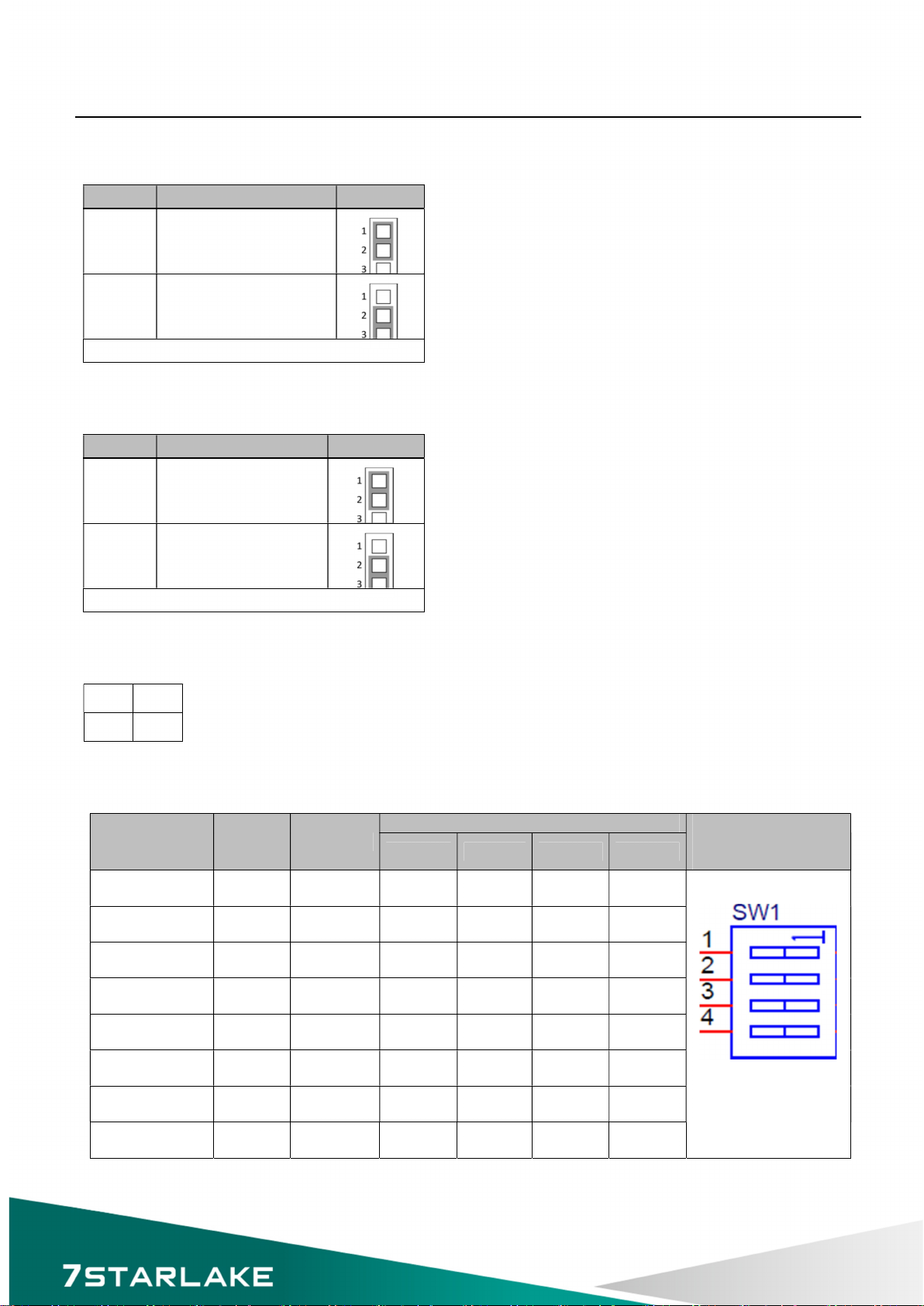
JP1: Clear CMOS .................................................................................................................................. 10
JP2: COM1 RI/+5V/+12V ...................................................................................................................... 10
JP14: mPCIe1 signal select .................................................................................................................. 11
JP15: mPCIe2 signal select .................................................................................................................. 11
JP24 LVDS Signal Power ..................................................................................................................... 11
SW1: LVDS Resolution ......................................................................................................................... 11
2.2.2 Connector ..................................................................................................................................... 12
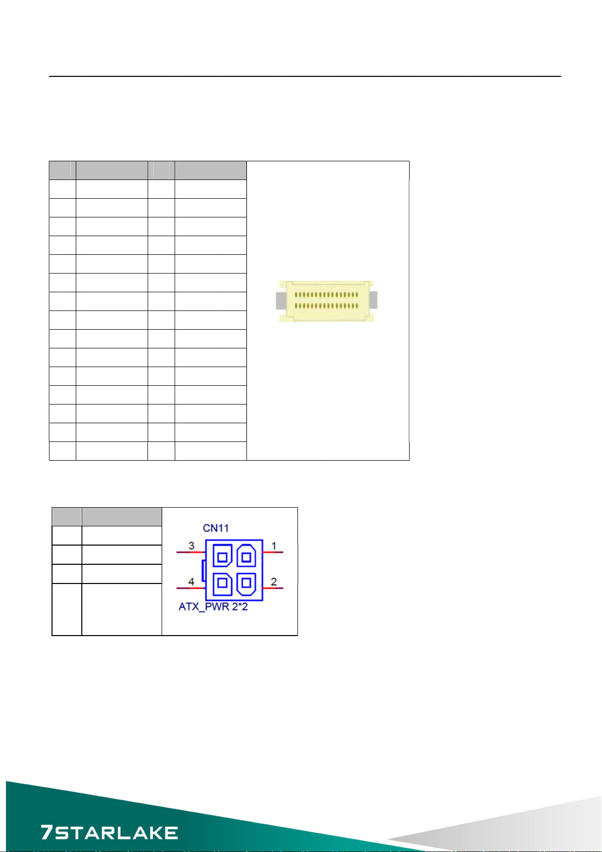
LVDS .................................................................................................................................................... 12
CN11: ATX Power ................................................................................................................................. 12
CN18: LVDS Control connector ......................................................................................................... 13
J1: DIO .................................................................................................................................................. 13
J6: SATA Power ................................................................................................................................... 13
J9: Front Panel ..................................................................................................................................... 14
J10: LPC ............................................................................................................................................... 14
J11: Audio ............................................................................................................................................. 14
COM1: RS232 with 5V/12V selectable ................................................................................................. 15
J12: COM2 RS232/422/485 ................................................................................................................. 15