Teledyne Lecroy PCI Express 5.0 U.2 User manual

PCI Express®5.0 U.2/U.3 12 Inch
Interposer CrossSync PHY Capable
User Manual and Quick Start Guide
Use this document for quick installation and setup.
Components
The interposer package includes the following components:
• PCI Express 5.0 U.2/U.3 12 inch Interposer
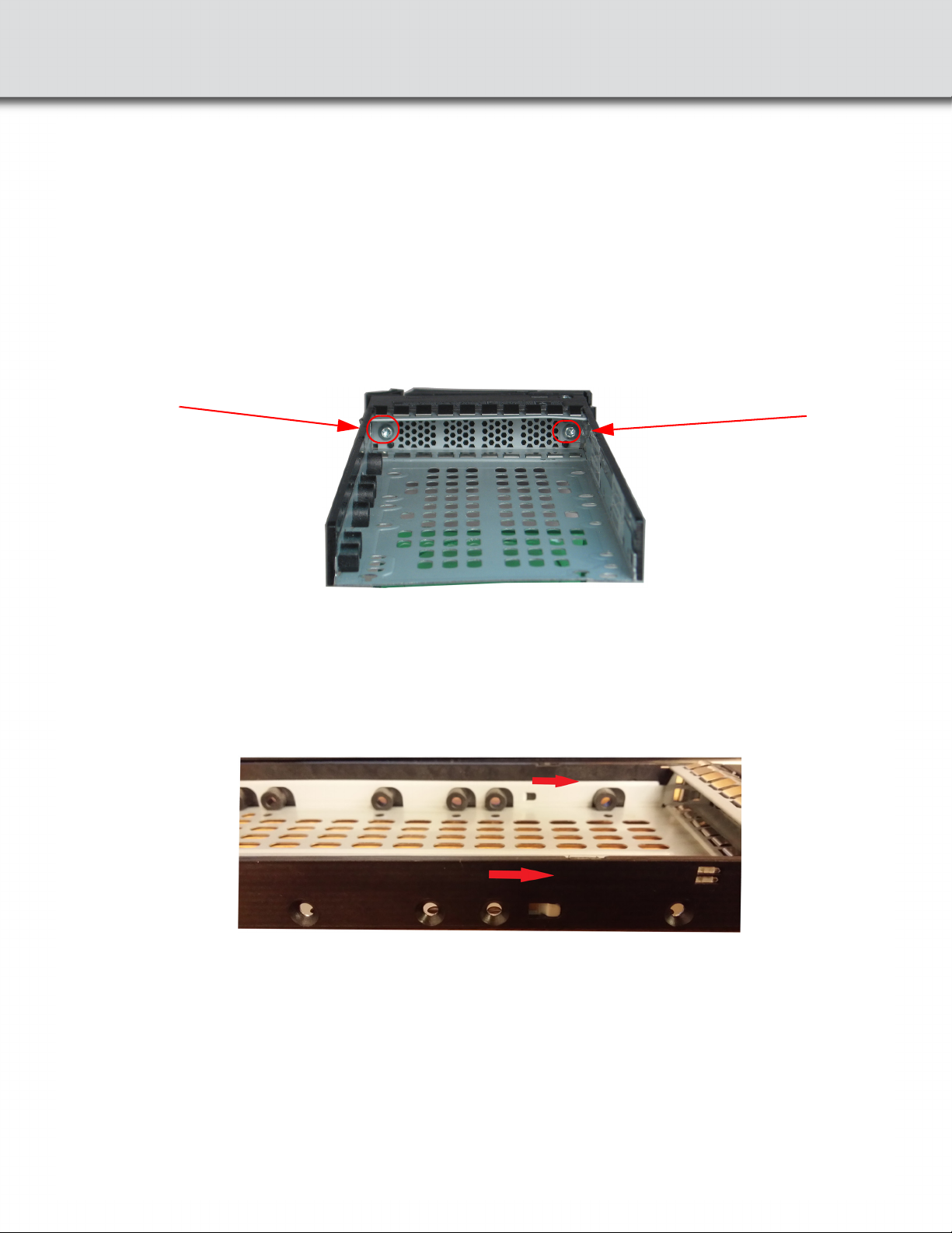
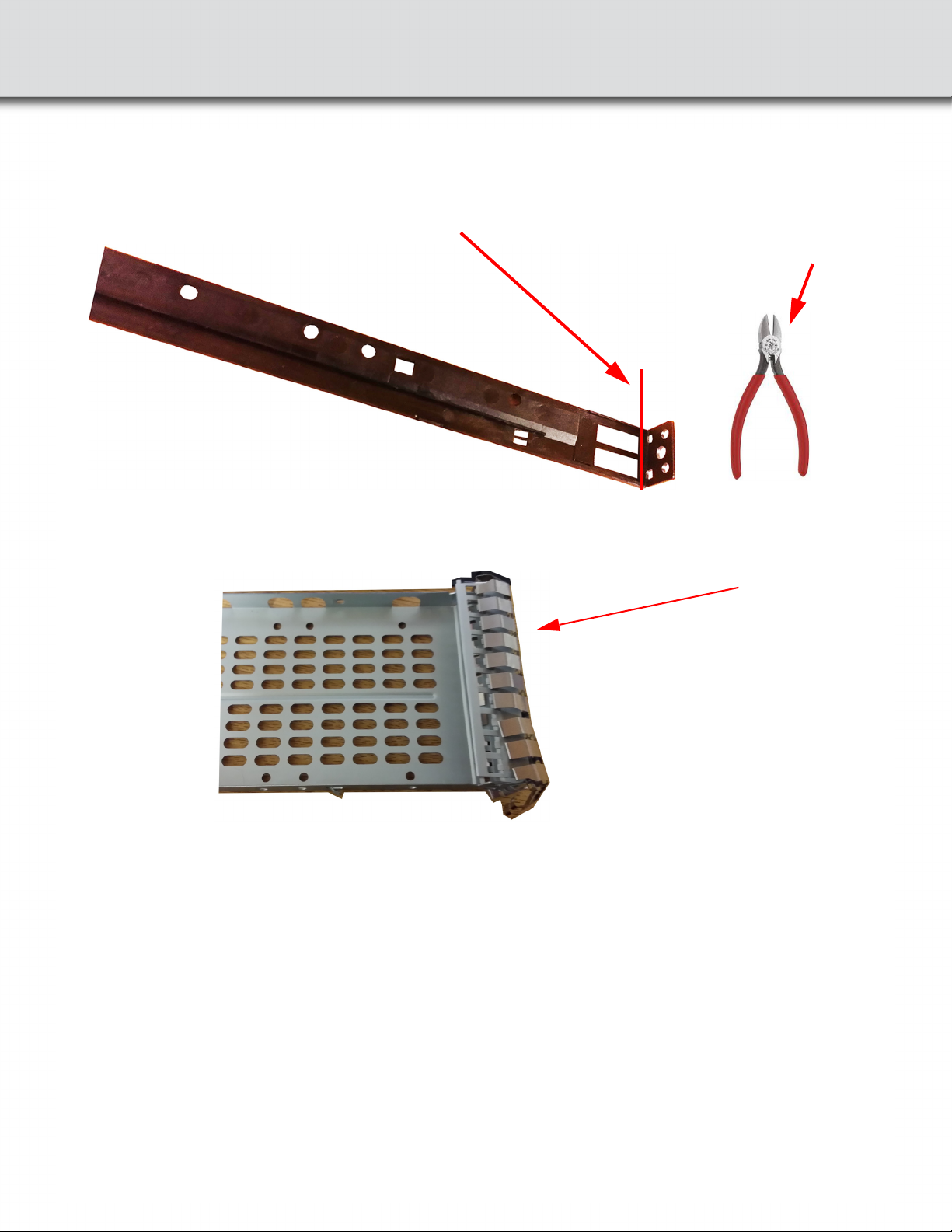
• 3.5 Inch conversion bracket and screws
• Two 90 degree conversion brackets and screws
• Support bracket for 7mm DUT and screws
• DC Power Adapter (+12V @ 5A)
• User Manual and Quick Start Guide (this document)
Inspect the received shipping container for any damage. Unpack the container and account for each of the system
components listed on the accompanying packing list. Visually inspect each component for absence of damage. In the
event of damage, notify the shipper and Teledyne LeCroy. Retain all shipping materials for shipper’s inspection.
Introduction
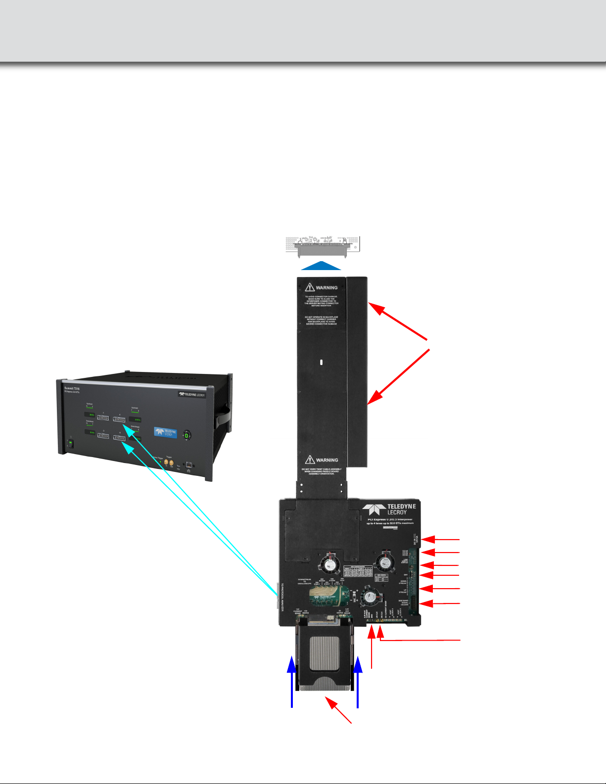
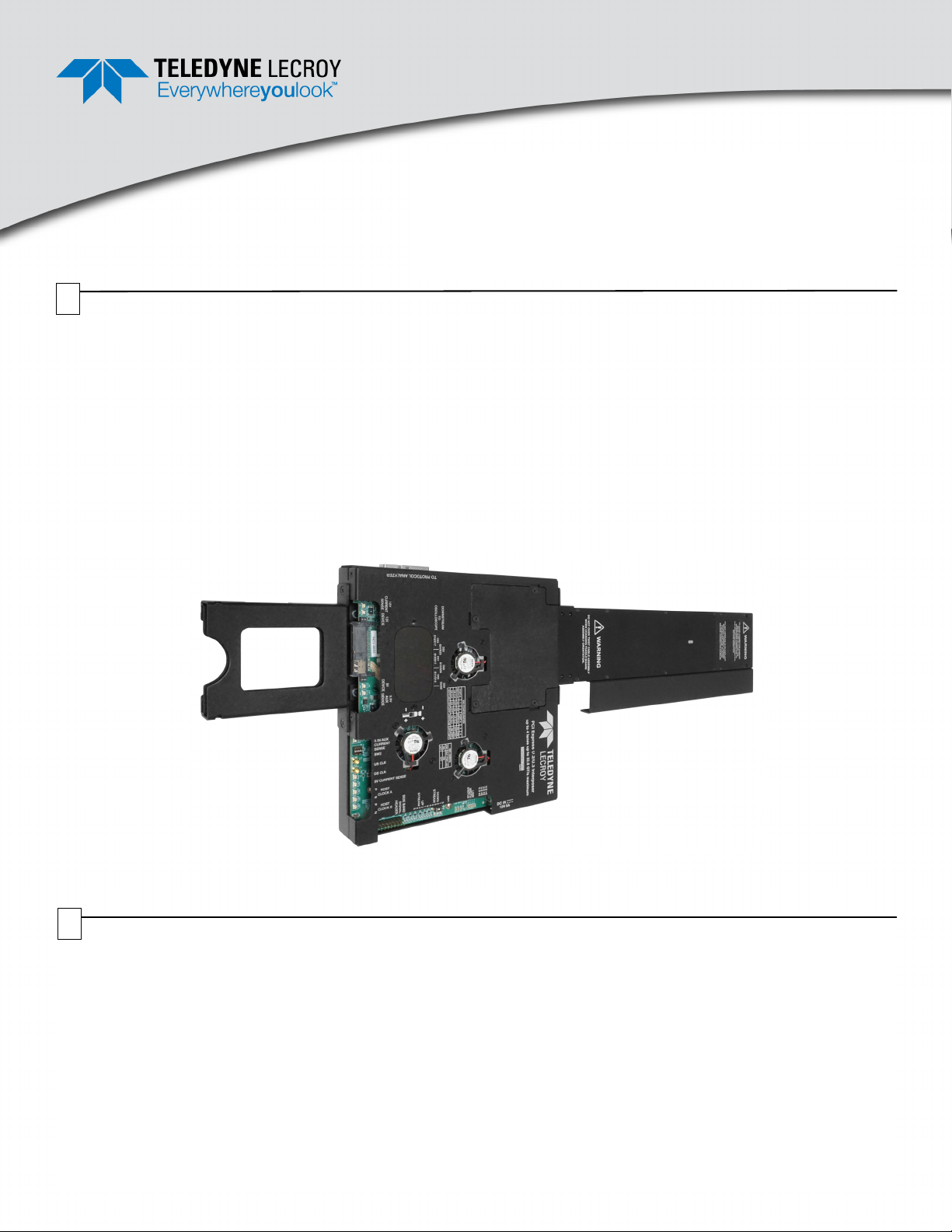
Teledyne LeCroy’s PCI Express 5.0 U.2/U.3 12 inch Interposer provides a quick and simple means for protocol analysis
of Solid State Drives (SSDs) based on PCI Express (PCIe®) protocols. The U.2/U.3 Interposer, used with a Summit
Protocol Analyzer, enables PCIe bus traffic between a host backplane and SSD device to be monitored, captured, and
recorded for protocol analysis. The card is compatible with the Summit T516 and Summit T54 and supports data rates
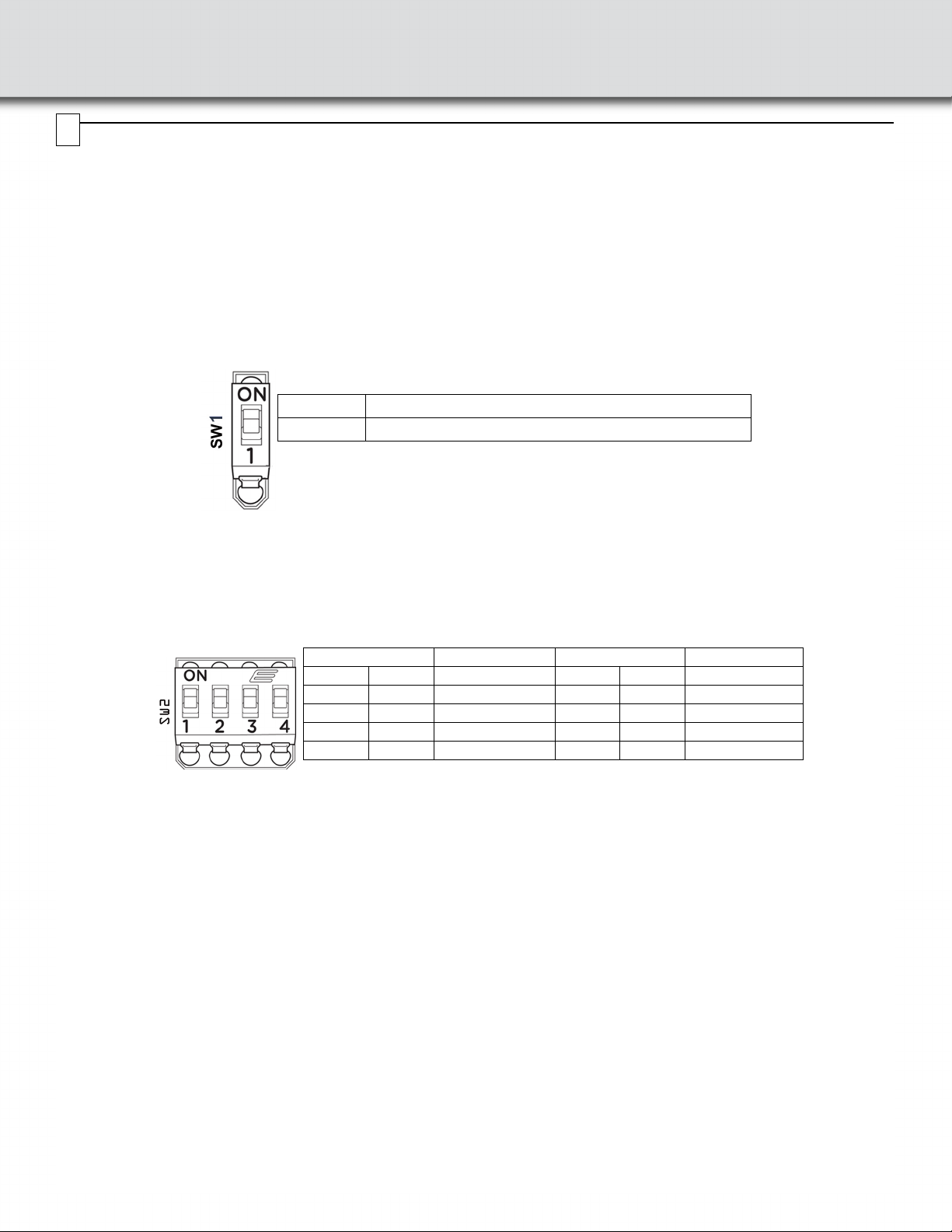
of 2.5 GT/s, 5.0 GT/s, 8.0 GT/s, 16.0 GT/s and 32 GT/s. The interposer supports side band signals such as PERST#,
WAKE#, CLKREQ# and SMBus (SMBCLK, SMBDAT). The interposer can be used with Single x4 Port or Dual x2 Ports.
It also supports U.2 and U.3 standards. It can be used also with Summit T4 and Summit M5x analyzers using a
conversion cable.
When the U.2/U.3 12 inch Interposer is upgraded with CrossSync PHY technology it will provide enhanced power
management and link training equalization debugging capability, enabling users to see and correlate both the physical
and protocol layers in a unified time aligned view. No other solution gives this type of insight into link behavior.
PCI Express 5.0 U.2/U.3 12 Inch Interposer
1
2

Switch Configurations
The source for the reference clock used by the analyzer to record PCI Express traffic is configurable according to below table. DIP
switches and tables for clock selection are located on the rear side of the interposer.
SW2:This switch changes clock settings.
SW1:This switch connects the DUT power Indication LED to the bus power.
SW1: DUT Power Status LEDs
ON LED Connected (Default)
OFF LED Disconnected
Note: In some systems with Hot-Plug management the Power Indication LEDs on the
interposer may prevent the host system from turning ON bus power to the device, if
this happens disconnect the LEDs using SW1 to allow proper bus power operation.
SW2: Clock Select SW2: Clock Select
12PortB 34PortA
ON ON REFCLKA ON ON REFCLKA
OFF ON US_CLK OFF ON US_CLK
ON OFF DS_CLK ON OFF DS_CLK
OFF OFF REFCLKB OFF OFF REFCLKB
Note: If using direct cable from Summit T516 refer only to table for Cable A for ports A and B.
Note: All switches in the ON position for SW2 is the factory default.
REFCLKA: Use the reference clock from Port A in the U.2 host connector.
US_CLK: Use the reference clock from the corresponding MMCX connector.
DS_CLK: Use the reference clock from the corresponding MMCX connector.
REFCLKB: Use the reference clock from Port B in the U.2 host connector.
3

Connections
IMPORTANT: If you plan to insert the interposer into a chassis backplane you MUST fit the rails from a donor
carrier to the interposer before use to avoid serious damage to the interposer. Instructions for
modifying a hard drive carrier are in Section 7.
Perform the following steps to connect the Interposer (see the image below):
1. Set the SW2 DIP switch to the desired positions to set the clock selection for Port A and Port B according to the table
above (see Section “3” on page ii).
2. Attach the interposer to a drive carrier (See Section “6” on page vi).
3. Install the U.2 or U.3 device under test (DUT) into the bay on the interposer as shown (will fit only 2.5” drives).
Screw the drive to the bay to secure it.
4. Install the Interposer into the host system connector.
5. Connect the Summit T516 Analyzer (or other compatible Teledyne LeCroy analyzer) to the interposer using
the appropriate analyzer cable (PE028UCA-X Y-cable or PE027UCA-X straight cable).
6. Connect the analyzer to a host computer system using the USB port on the front panel of the Summit analyzer.
7. If not already done, install the PCIe Protocol Analysis software on the host machine.
8. Connect 12V DC using the AC adapter supplied with the interposer to the Gen5 U.2/U.3 interposer. Make sure that
the AC adapter is powered on before proceeding to the next step.
9. Power on the analyzer.
10. Launch the PCIe Protocol Analysis application, setup the appropriate recording options and start a recording.
For more information see the PCI Express Protocol Analysis Summit T5 Gen5 Analyzer User Manual →
Recording Options →Select Interposer Type section.
11. Power on the host machine.
12. Use the PCIe Protocol Analysis application to monitor, record and view PCI Express traffic passing through
the U.2 Interposer.
Note: For more connection examples see the Summit T5 PCI Express Gen5 User Manual.
Note: We are continuously improving and releasing new products. For new interposers to operate optimally always
check the Teledyne LeCroy website for the latest version of the PCIe Protocol Analysis Software.
4

Analyzer Y cable:
PE028UCA-X
Summit T516 Analyzer
12V DC from
adapter supplied
External Clock Inputs MMCX
(Optional Connection)
Device Under Test
(DUT)
Lane Activity LEDs
SW2: Clock Selection
SW1: DUT Power Status LEDs
Link Standard Detection LEDs
Attach support
bracket for 3.5
Inch conversion
(optional) and
drive carrier
(required). See
sections 7 and 8
below.
J28:Sideband Signal Header
A
B
U.2/U.3 Host Slot
Link Width Status LEDs
Connecting the PCI Express 5.0 U.2/U.3 12 Inch Interposer to one Summit T516 Analyzer

Sideband Header Pinout
Table 1: J28 Sideband Header
Table 2: Test Point Numbers and Names
Header Pin Number Sideband Signal Name
J28-1 WAKE#
J28-2 IFDET#2
J28-3 CLKREQ#
J28-4 HPT0
J28-5 IFDET#
J28-6 HPT1
J28-7 PRSNT#
J28-8 SMCLK
J28-9 ACTIVITY#
J28-10 SMDAT
J28-11 PCIEB_RST#
J28-12 DUALPORTEN#
J28-13 PCIEA_RST#
J28-14 DEV_RESET
J28-15 GND
J28-16 GND
Test Point Number Test Point Name
TP7 P12V_DEVICE
TP16 12V DC JACK
TP21 5V
J34 P3P3V_AUX_HOST
J36 P12V_HOST
J35 P5V_HOST
TP38 3.65V Switching REG OUT
TP45 1.2V Core
TP46 1.2V IO
TP49 1.8V IO
TP50 2.5V Core
TP53 2.5V IO
TP58 3.3V, Downstream ADI LDO
TP60 3.3V, Upstream ADI LDO
TP62 3.3V IO
5

Modification of HDD Carrier for Use with the PCIe 5.0 U.2/U.3 12 Inch Interposer
Warning: DO NOT OPERATE IN A CHASSIS WITHOUT ADDING CARRIER RAILS OR YOU WILL DAMAGE THE
INTERPOSER.
Teledyne LeCroy's PCI Express 5.0 U.2/U.3 Interposer can be attached to a donor drive carrier. If you plan to insert the
interposer into a Chassis backplane you MUST fit the rails from a donor carrier to the interposer before use, to avoid
serious damage to the interposer. In order to do this, some adjustments need to be made to the drive carrier to allow the
interposer to fit properly. Teledyne LeCroy provides these instructions as a service to users but any modification done
to the drive carrier is done at the user’s risk. Teledyne LeCroy provides no guarantee or warranty with these
modifications. These modifications of the drive carrier are the sole responsibility of the user. This procedure is for this
specific drive. carrier. Other drive carriers may need slightly different steps, but this drive carrier is typical. See the
following figures.
Drive Carrier
Ejection Catch Assembly
6

Step 1. Remove the Drive Carrier from the Server Backplane
To remove the drive carrier from the server backplane, squeeze the two levers together on the front of the carrier and
while gripping the handle provided on the front of the carrier slowly pull the drive carrier out of the server backplane.
Set the drive carrier on a suitable work surface (workbench with ESD pad or similar surface).
Step 2. Remove the Ejection Catch Assembly from the Drive Carrier
To remove the ejection catch assembly, remove two screws holding the metal housing to the ejector catch assembly on
the front of the drive carrier.
Screws holding Ejection Catch to Drive Carrier
Top
Screw Bottom
Screw
Step 3. Remove the Side Runners and Light Pipes from the Drive Carrier
To remove the side runners and light pipes from the drive carrier, slide the black plastic runners towards the back and
lift away from the retaining lugs. Retain the black plastic runners for reuse.

Step 4. Remove the Corner of the Side Rail After Removal from Drive Carrier
Using a suitable cutting tool (diagonal cutting pliers, etc) remove the corners of the side rails.
Step 5. Remove the EMI Shield Springs
The EMI spring system should be gently pulled away and unclipped from the end of the drive carrier. It will not be reused.
Cut along the corner
of the side rail
Typical set of
diagonal
cutting pliers
(or similar tool)

Step 6. Bend Drive Carrier Ears Out of the Way
The drive carrier is usually a simple folded piece of fairly thin metal, which can be gently bent flat by hand. If there are
metal ears, which held the screws to the ejection catch assembly, they should be gently (by hand) unfolded first before
the end of the drive carrier metal is unfolded.
Step 7. Bend Drive Carrier Metal End Out Flat
Gently (by hand) bend the metal end of the drive carrier out flat.
Step 8. Re-Attach the Plastic Side Rails
After the Side Rail corners have been removed, the side rails can be reattached using the original screws.
Ear bent out
of the way

Step 9. Attach the PCI Express 5.0 U.2/U.3 12 Inch Interposer to the Drive Carrier
Slide the Interposer into the drive carrier, using the original mounting screws to hold it in place. The Interposer should be aligned with
the same holes the drive carrier would have used. Note: Screw type for use with Drive Carrier: Metric screw, size M3, maximum
length: 8mm.
Step 10. Attach Cabling to the Interposer
Insert the carrier with the Interposer into the desired backplane slot. Plug one end of the interposer cable to the
Interposer and other end into the analyzer. Attach the 12VDC power and optional clock cables.
This completes the assembly of the Interposer into the Drive Carrier.

Support Bracket for 3.5 Inch Conversion
To support and stabilize the PCI Express 5.0 U.2/U.3 Interposer within a 3.5" drive carrier, Teledyne LeCroy supplies a
bracket kit. The bracket can be mounted on either the top or bottom of the Interposer, depending on the drive carrier
configuration. Teledyne LeCroy’s interposer with the 3.5 inch bracket attached is shown below.
To install the bracket on either side of the Interposer, three screws are provided.
1. Set out the Interposer, bracket and mounting screws as shown below:
2. Using a small Phillips head screw driver insert each screw through the appropriate hole in the bracket.
3. Insert each of the two screws into a threaded hole in the Interposer.
4. Tighten each screw so that the bracket is held firmly to the top or bottom of the Interposer (as shown below).
Support bracket
Gen5 U.2 Interposer
Gen5 U.2 Interposer
Support bracket
7

Bracket extension installed on the left side of the interposer
Bracket extension installed on the right side of the interposer
Gen5 U.2 Interposer
Support bracket
Gen5 U.2 Interposer
Support bracket

Support Bracket for 7mm DUT
To support and stabilize the PCI Express 5.0 U.2/U.3 Interposer within a 3.5" drive carrier, Teledyne LeCroy supplies a
bracket kit. The bracket can be mounted on either the top or bottom of the Interposer, depending on the drive carrier
configuration. Teledyne LeCroy’s interposer with the 3.5 inch bracket attached is shown below.
To install the bracket on either side of the Interposer, two screws are provided.
1. Set out the Interposer, bracket and mounting screws as shown below:
2. Using a small Phillips head screw driver insert each screw through the appropriate hole in the bracket.
3. Insert each of the two screws into a threaded hole in the Interposer.
4. Tighten each screw so that the bracket is held firmly to the top or bottom of the Interposer (as shown below).
Support bracket
Gen5 U.2 Interposer
Support bracket
8

Support bracket installation complete

CrossSync Capability
The PE221UIA-X PCI Express 5.0 U.2/U.3 12 inch Interposer includes CrossSync PHY capability, enabling:
• Easy signal access to sideband signals, power rail and refclk probing points
• Optional PE130ACA-X upgrade adds preinstalled connections on data lanes for Teledyne LeCroy DH Series
high-bandwidth differential oscilloscope probes
• Optional CrossSync PHY oscilloscope software adds time-synchronization and integrated cross-analysis
between PETracer protocol analysis software and MAUI oscilloscope software
The figures below show the location of the CrossSync PHY oscilloscope probing points on the interposer (version with
PE130ACA-X upgrade pictured).
Oscilloscope probing points on CrossSync PHY enabled interposer – front view
Downstream
high-speed signal
probing points
(Optional with
PE130ACA-X
upgrade)
Rail voltage and
current probing points
Sideband signal
probing points
REFCLK probing
points
9

Oscilloscope probing points on CrossSync PHY enabled interposer - rear view
Upstream
high-speed signal
probing points
(Optional with
PE130ACA-X
upgrade)

Connecting Probes to Sideband Signals
Sideband signals are available on standard square header pins in the location shown in first figure above, with pinout
detailed in “J28 Sideband Header” on page v. These may be probed with a standard passive or active high-impedance
oscilloscope probe.
Available sideband signals include: WAKE#, IFDET#2, CLKREQ#, HPT0, IFDET#, HPT1, PRSNT#, SMCLK, ACTIVITY#,
SMDAT, PCIEB_RST#, DUALPORTEN#, PCIEA_RST# and DEV_RESET. Specific pins are labeled directly on the circuit
board for reference.
Connecting to Rail Voltage and Current Monitoring Points
Rail voltage and current points are available on UMC connectors in the location shown in the interposer front view diagram
above. These are best probed with an RP4030 voltage rail probe, but connection directly to a coaxial oscilloscope input is
also possible.
Voltage and current can be monitored for the 5V, 3.3Vaux and 12V rails. The voltage points are connected directly to the
voltage being supplied from the host to the endpoint. The current monitoring point for 3.3Vaux operates at a conversion
factor of 1A →1V, the point for 5V operates at a conversion factor of 1.5A →1V and the current points for 12V operate at a
conversion factor of 2A →1V (see the oscilloscope's manual or online help for details).
Connecting to Reference Clock Probing Points
Reference clock activity can be monitored on UMC connectors in the location shown in the first figure above. Reference
clock probing points can be connected directly to a 50 Ωoscilloscope input. This reference clock signal has been buffered
so that it does not connect directly to the host's reference clock.
Connecting Probes to High-speed Signals
With the PE130ACA-X CrossSync PHY upgrade, the interposer exposes 12 connections for high-speed probes, allowing
any of the upstream or downstream lanes to be probed as desired.
High-speed signal probing points are designed exclusively for Teledyne LeCroy DH series high-bandwidth differential
probes. A special probe lead, the DH-CSPHY-PCIE5-U2-U3, is used to create the connection between amplifier and
interposer. See the figures below.
Connect DH-CSPHY-PCIE5-U2-U3 lead to Teledyne LeCroy DH series high-bandwidth differential oscilloscope
probe

Connect DH-CSPHY-PCIE5-U2-U3 lead to desired lane on interposer
A polarity indication is printed directly on the interposer next to the probing points (see figure below)- this indicates the side
of the connector that should align with the side of the DH-CSPHY-PCIE5-U2-U3 denoted by a white indicator. Note that
since devices in a PCIe link may invert polarity of any given lane, this indication on the interposer and probe is provided for
consistency, and not as an absolute indication of signal polarity.

Recommended Oscilloscope Options
Oscilloscope Probes
Oscilloscope Software Options
The Oscilloscope Software options allow you to enable CrossSync PHY functionality on installed CrossSync software.
Product Description Product Code
High-speed Data Signals
8 GHz differential probe with ProLink interface DH08-PL
13 GHz differential probe with ProLink interface DH13-PL
16 GHz differential probe with ProLink interface DH16-PL
20 GHz differential probe with ProLink interface DH20-PL
25 GHz differential probe with 2.92 mm interface DH25-2.92MM
30 GHz differential probe with 2.92 mm interface DH30-2.92MM
Rail voltage/current points
Voltage Rail Probe - 4 GHz bandwidth, 1.2x attenuation, ±30V offset RP4030
Product Description Product Code
CrossSync PHY option for LabMaster 10 Zi - sync oscilloscope with PCIe
Protocol Analyzer hardware
LM10Zi-CrossSyncPHY
CrossSync PHY option for WaveMaster 8 Zi - sync oscilloscope with PCIe
Protocol Analyzer hardware
WM8Zi-CrossSyncPHY
10

Recommended Oscilloscopes
CrossSync PHY is compatible with all LabMaster 10 Zi and WaveMaster 8 Zi series oscilloscopes. Below are some
recommendations for example test configurations.
PCI Express 3.0 - CrossSync PHY and Compliance Test Capable
PCI Express 4.0 - CrossSync PHY and Compliance Test Capable
PCI Express 5.0 - CrossSync PHY and Compliance Test Capable
Product Description Product Code
13 GHz (or higher), 40 GS/s, 4ch, 64 Mpts/Ch Serial Data Analyzer with 6.5
Gb/s Serial Trigger, 8b/10b and 64b/66b decode.
SDA 813Zi-B
QualiPHY PCIe 3.0 Compliance Software Option QPHY-PCIE3-TX-RX
Product Description Product Code
25 GHz (or higher) 80 GS/s LabMaster 10 Zi Acquisition Module LabMaster 10-25Zi-A
LabMaster Master Control Module LabMaster MCM-Zi-A
QualiPHY PCIe 4.0 Compliance Software Option (Also includes PCIe 3.0
compliance)
QPHY-PCIE4-TX-RX
2.92mm to ProBus Adapter for connecting RP4030 and passive probes to
LabMaster acquisition module
L2.92A-PBUS
1 MΩadapter – used with L2.92A-PBUS for connecting passive probes to
LabMaster acquisition module
AP-1M
Product Description Product Code
50 GHz (or higher) 160 GS/s LabMaster 10 Zi Acquisition Module LabMaster 10-50Zi-A
LabMaster Master Control Module LabMaster MCM-Zi-A
QualiPHY PCIe 5.0 Compliance Software Option (Also includes PCIe 3.0
and 4.0 compliance)
QPHY-PCIE5-TX-RX
2.92mm to ProBus Adapter for connecting RP4030 and passive probes to
LabMaster acquisition module
L2.92A-PBUS
1 MΩadapter – used with L2.92A-PBUS for connecting passive probes to
LabMaster acquisition module
AP-1M
Other manuals for PCI Express 5.0 U.2
1
This manual suits for next models
1
Table of contents
Other Teledyne Lecroy Diagnostic Equipment manuals