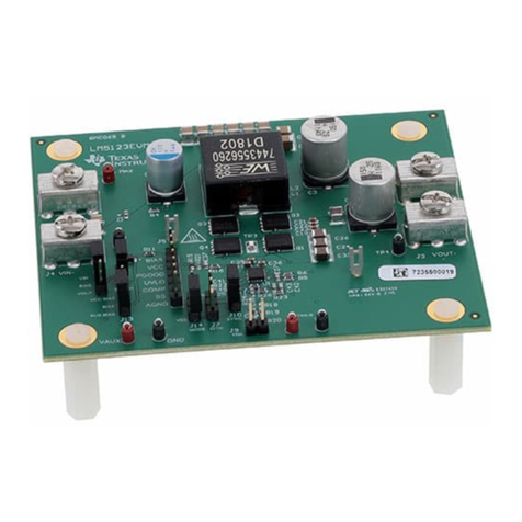
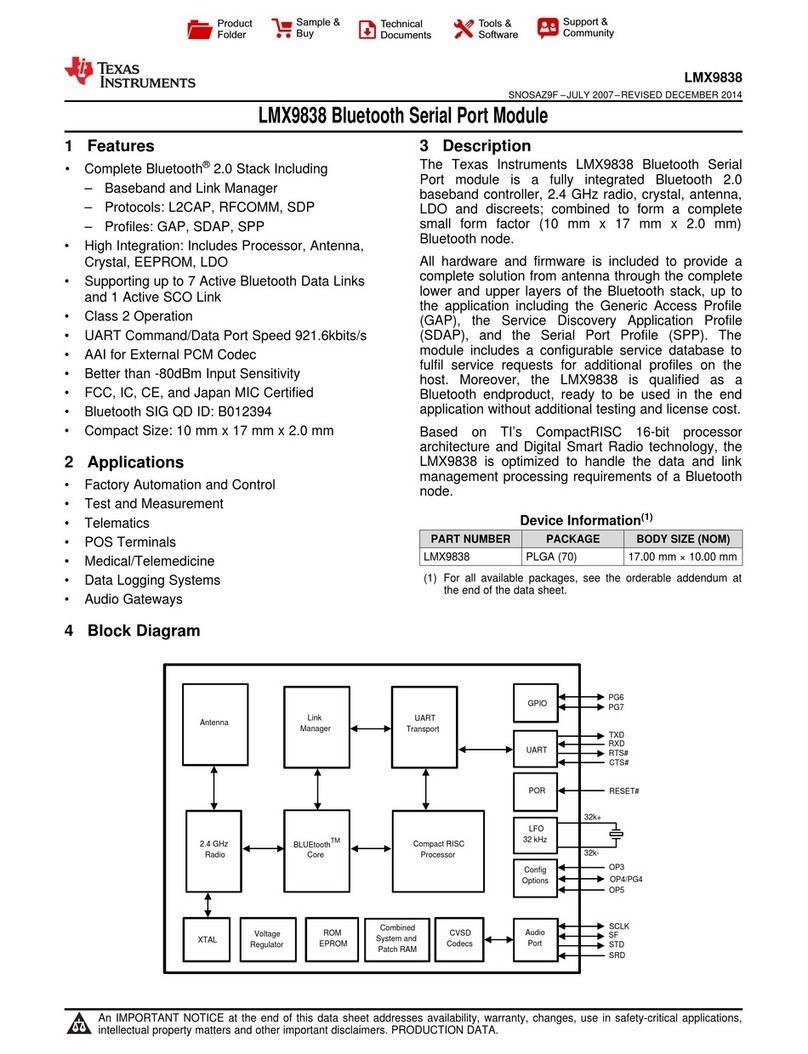
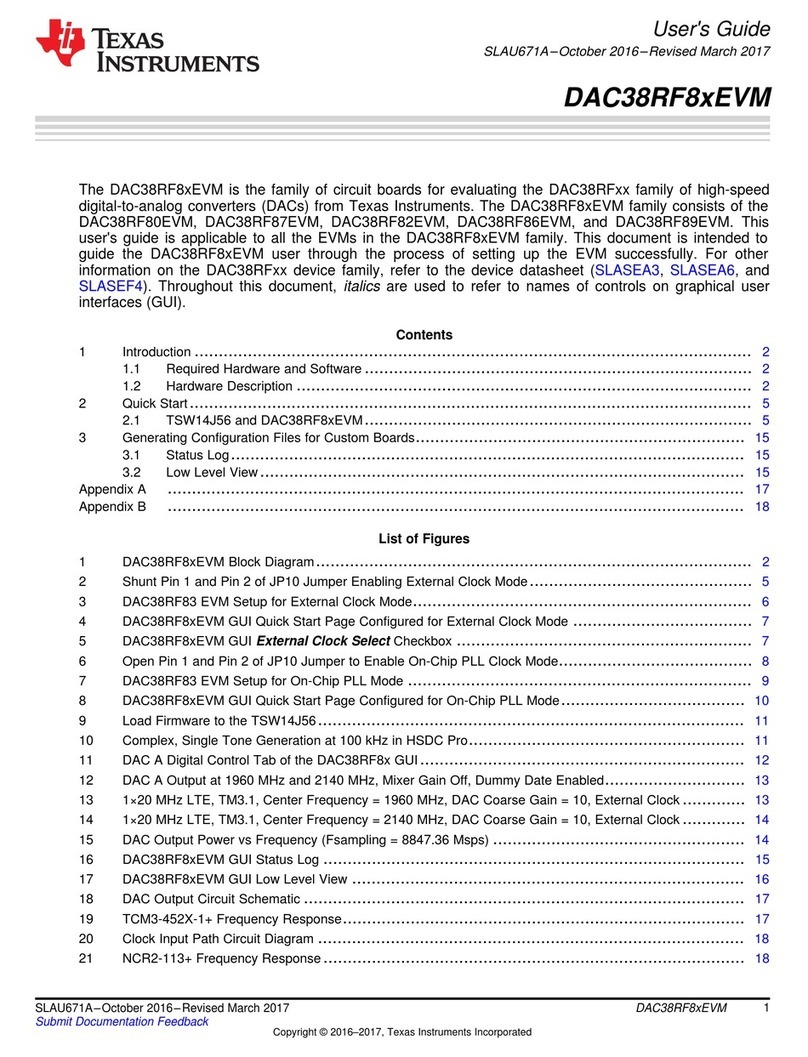
Texas Instruments 990 User manual
Other Texas Instruments Control Unit manuals
Texas Instruments
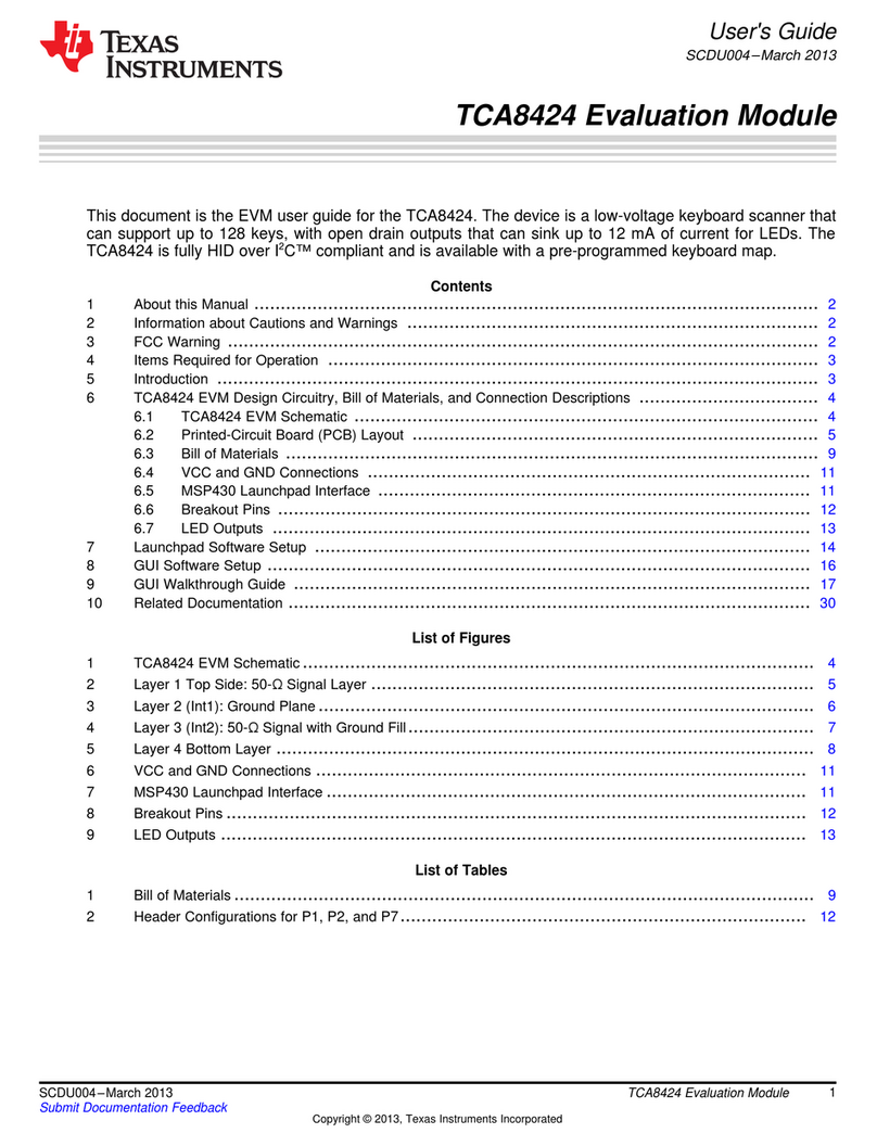
Texas Instruments TCA8424 User manual
Texas Instruments
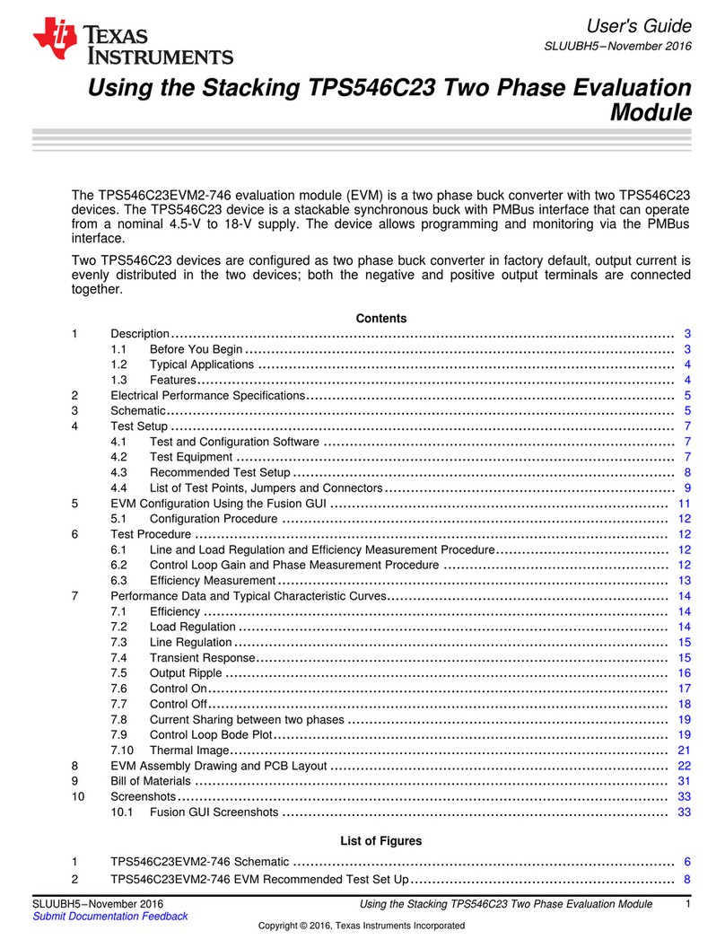
Texas Instruments TPS546C23 User manual
Texas Instruments
Texas Instruments UCC28740EVM-525 User manual
Texas Instruments
Texas Instruments HSS-MOTHERBOARDEVM User manual
Texas Instruments
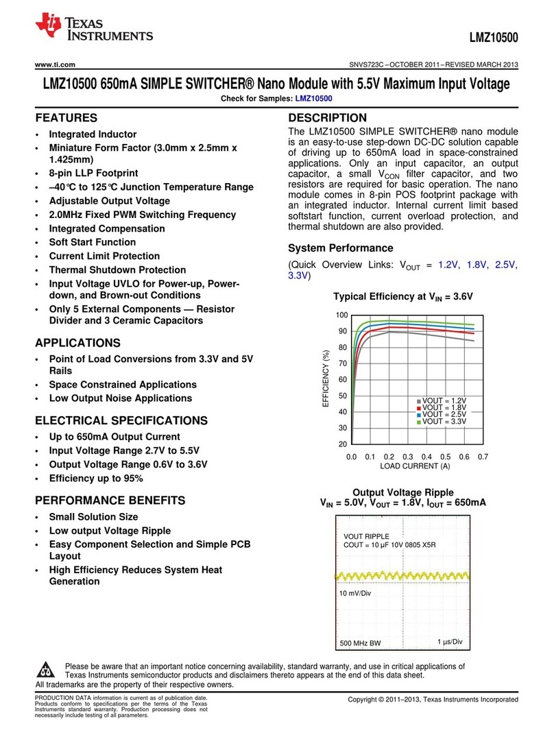
Texas Instruments AN-2166 LMZ10500 User manual
Texas Instruments
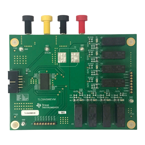
Texas Instruments TLC6A598 User manual
Texas Instruments
Texas Instruments CDCM9102EVM User manual
Texas Instruments
Texas Instruments BOOSTXL-CAPKEYPAD User manual
Texas Instruments
Texas Instruments DS160PR412-421EVM User manual
Texas Instruments
Texas Instruments TAS5086-5186V6EVM User manual
Texas Instruments
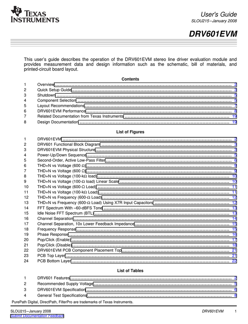
Texas Instruments DRV601EVM User manual
Texas Instruments
Texas Instruments TPA0142 User manual
Texas Instruments
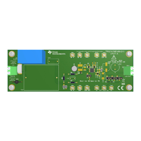
Texas Instruments TPS7A78EVM-011 User manual
Texas Instruments
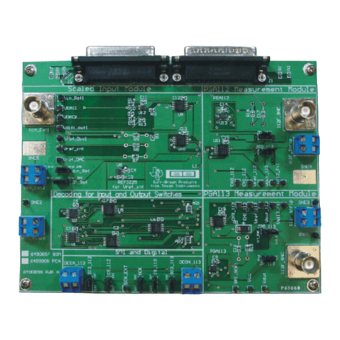
Texas Instruments PGA112 User manual
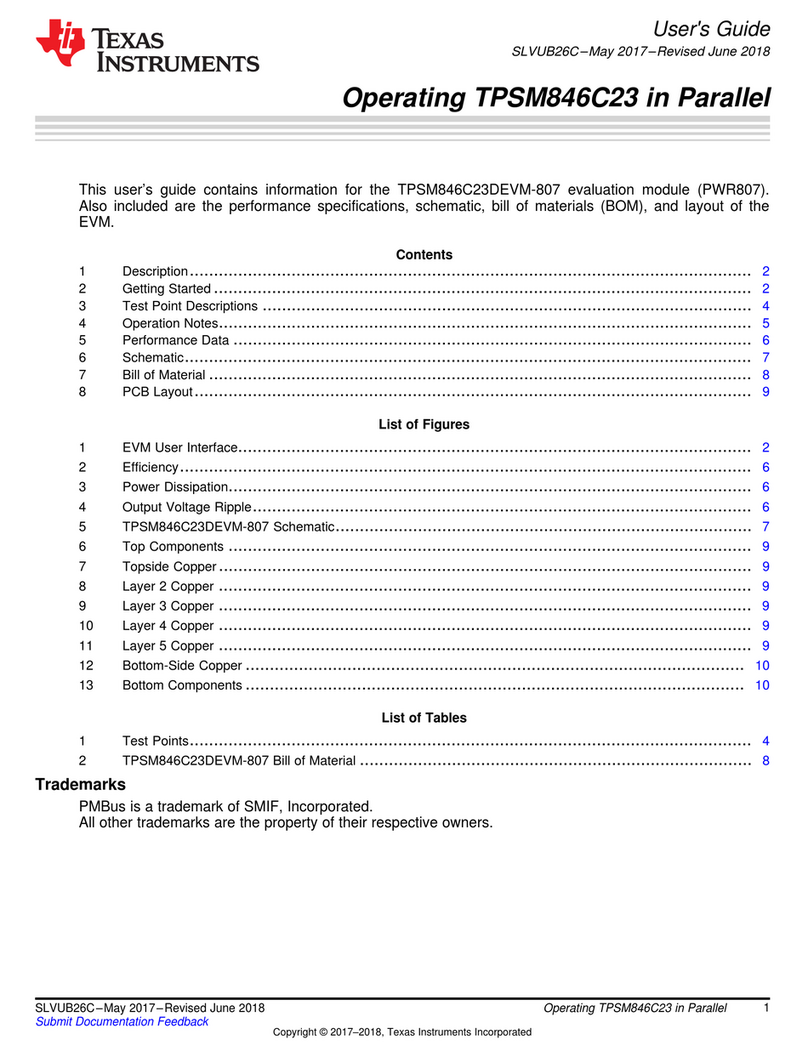
Texas Instruments
Texas Instruments TPSM846C23 User manual

Texas Instruments
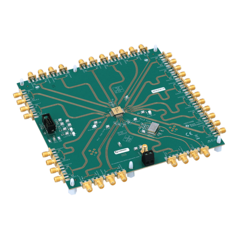
Texas Instruments TPS54383 User manual
Texas Instruments
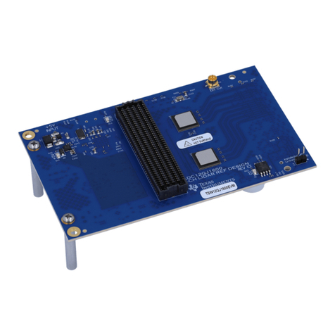
Texas Instruments LMK04832EVM-CVAL User manual
Texas Instruments
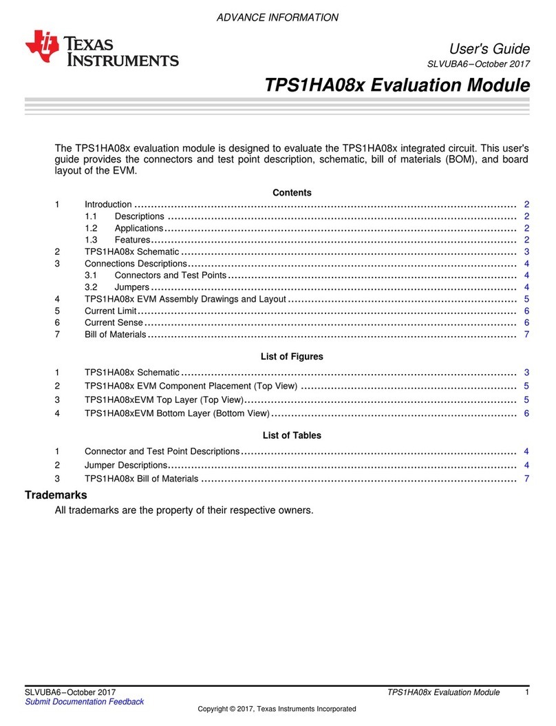
Texas Instruments TSW12QJ1600 User manual
Texas Instruments
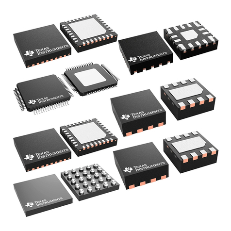
Texas Instruments TPS1HA08x User manual
Texas Instruments
Texas Instruments BQ24180 User manual
Popular Control Unit manuals by other brands
Festo
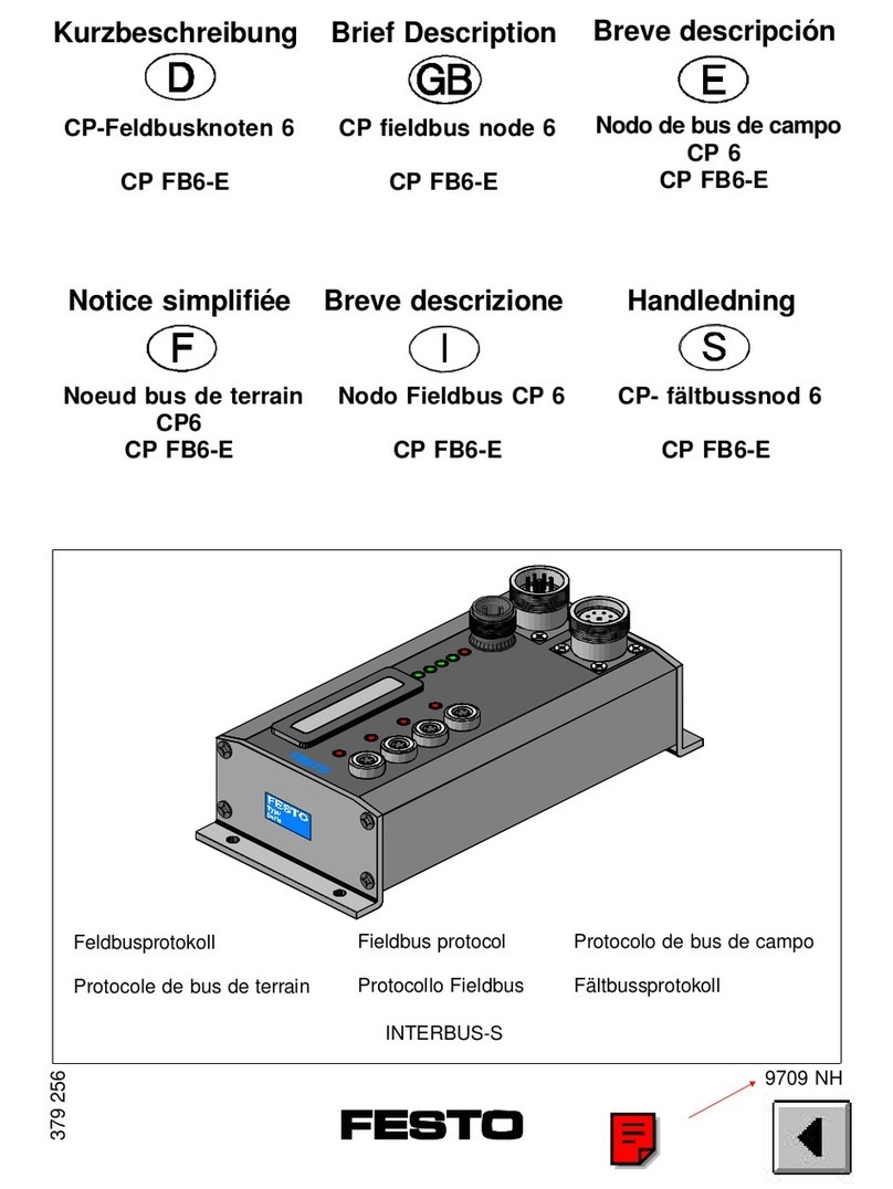
Festo Compact Performance CP-FB6-E Brief description
Elo TouchSystems
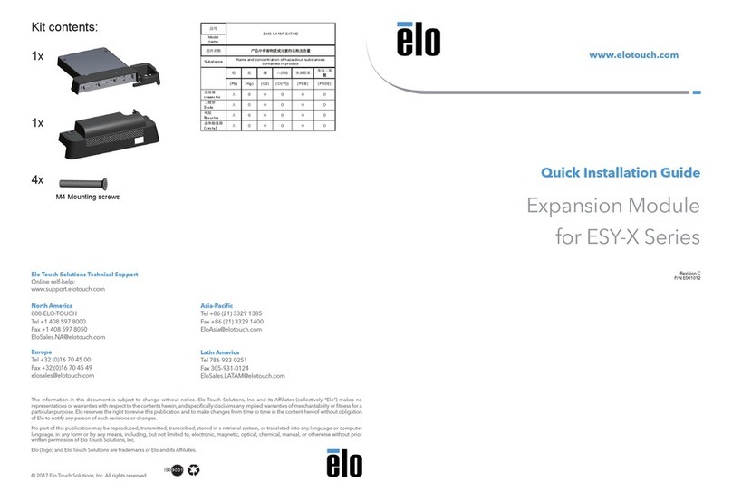
Elo TouchSystems DMS-SA19P-EXTME Quick installation guide
JS Automation
JS Automation MPC3034A user manual
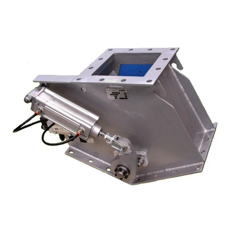
JAUDT
JAUDT SW GII 6406 Series Translation of the original operating instructions
Spektrum
Spektrum Air Module System manual
BOC Edwards
BOC Edwards Q Series instruction manual

KHADAS
KHADAS BT Magic quick start
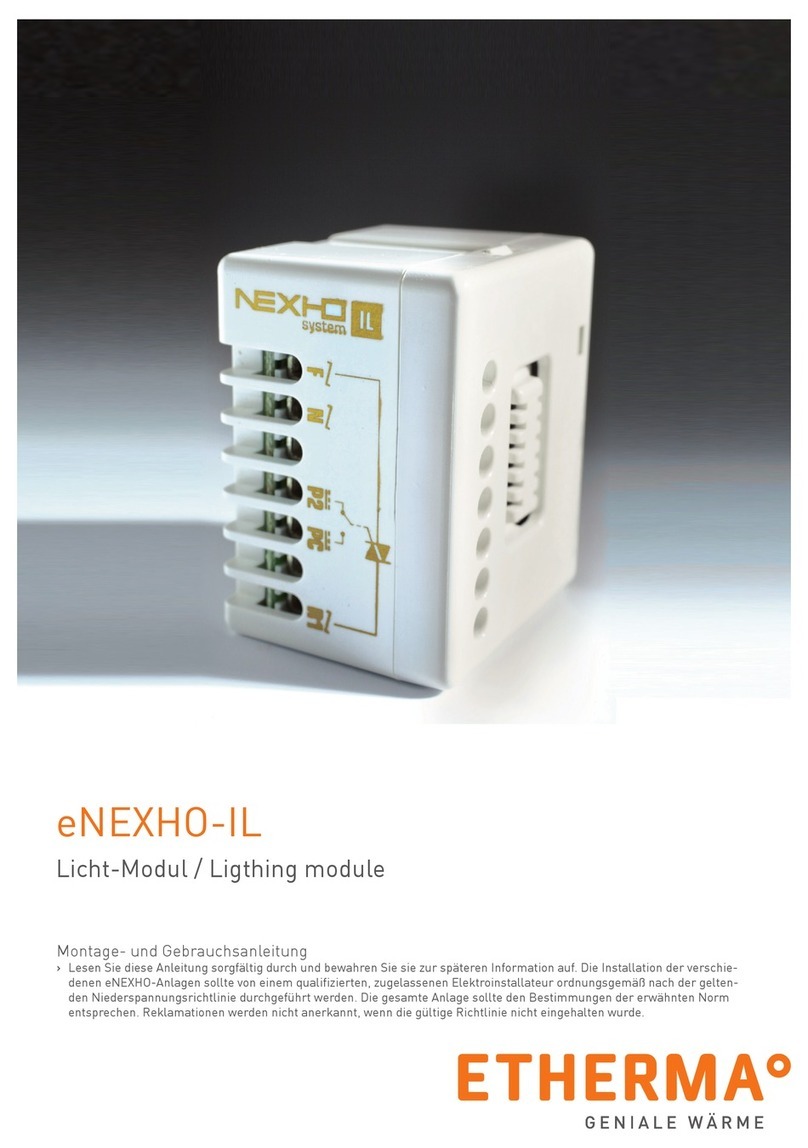
Etherma
Etherma eNEXHO-IL Assembly and operating instructions
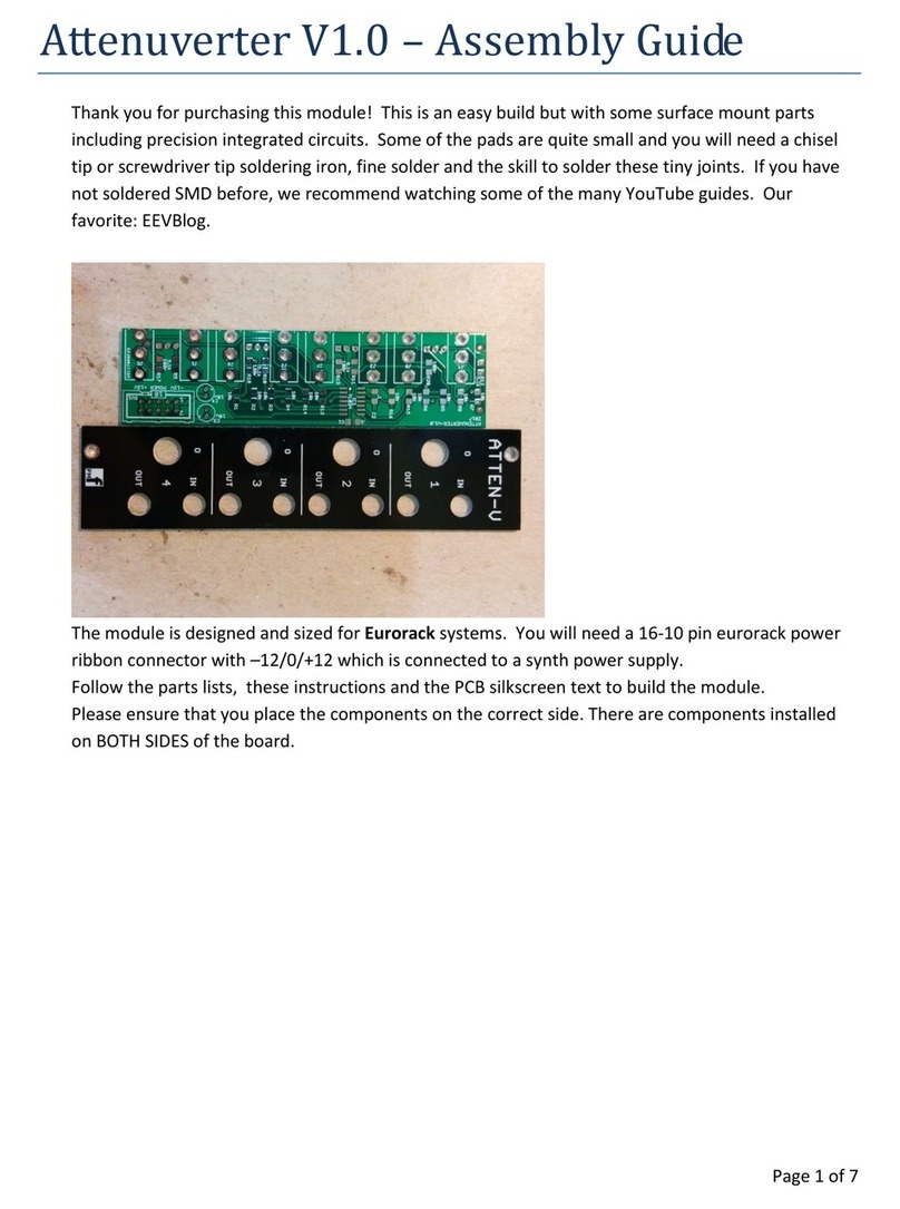
PMFoundations
PMFoundations Attenuverter Assembly guide
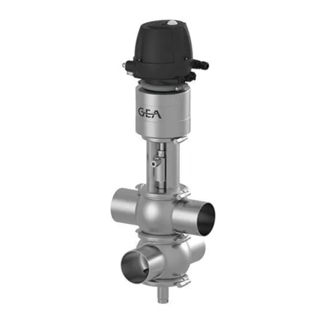
GEA
GEA VARIVENT Operating instruction
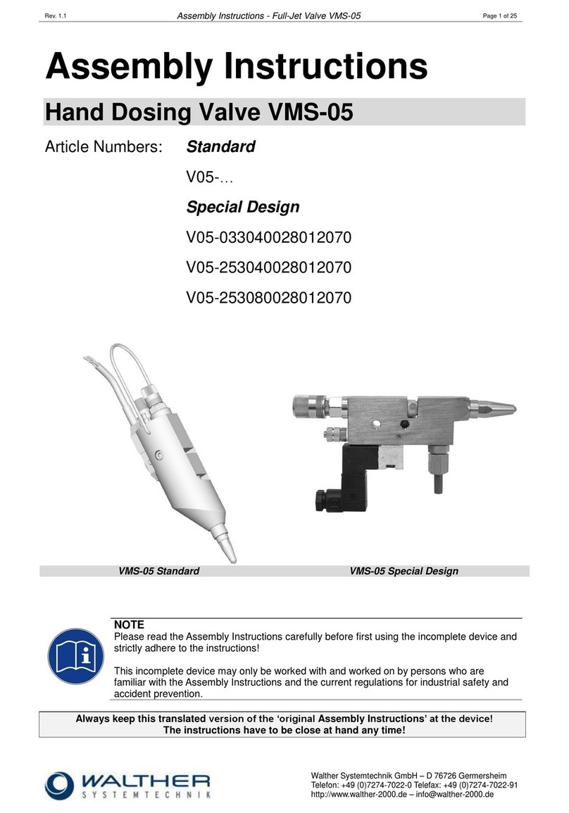
Walther Systemtechnik
Walther Systemtechnik VMS-05 Assembly instructions
Altronix
Altronix LINQ8PD Installation and programming manual
