Texas Instruments TRF7960A User manual
Other Texas Instruments Control Unit manuals
Texas Instruments
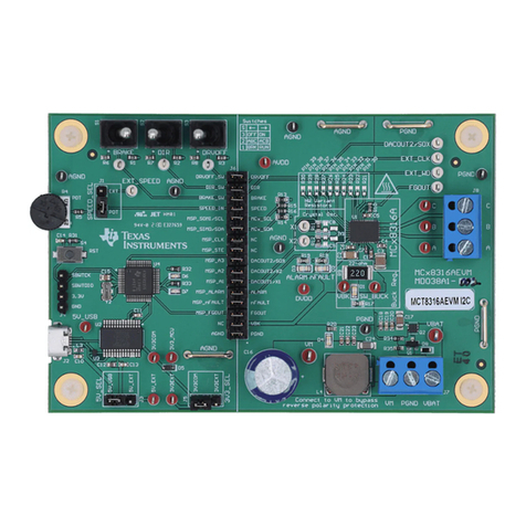
Texas Instruments MCT8316AEVM User manual
Texas Instruments
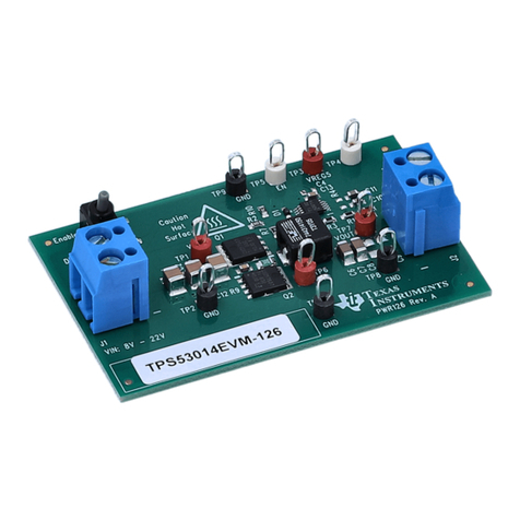
Texas Instruments TPS53014 User manual

Texas Instruments
Texas Instruments ADC12DL 00 Series User manual
Texas Instruments
Texas Instruments bq2022A User manual
Texas Instruments
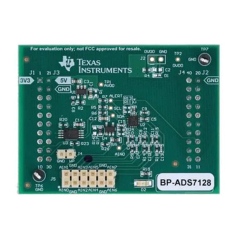
Texas Instruments BoosterPack BP-ADS7128 User manual
Texas Instruments
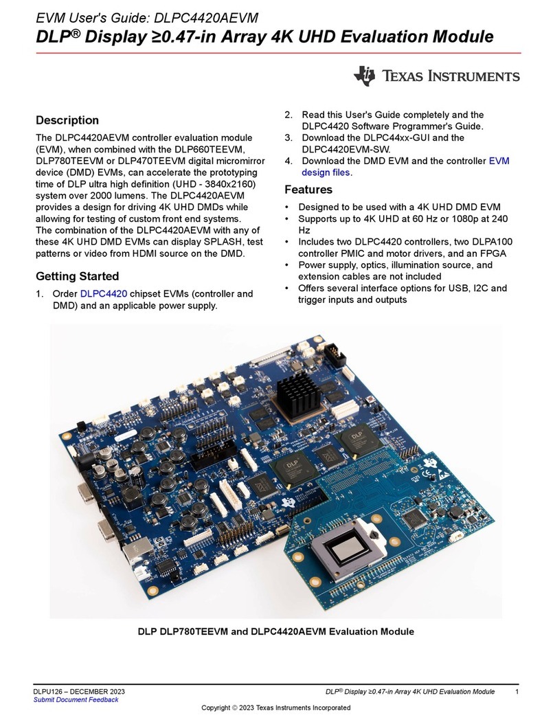
Texas Instruments DLP DLPC4420AEVM User manual
Texas Instruments
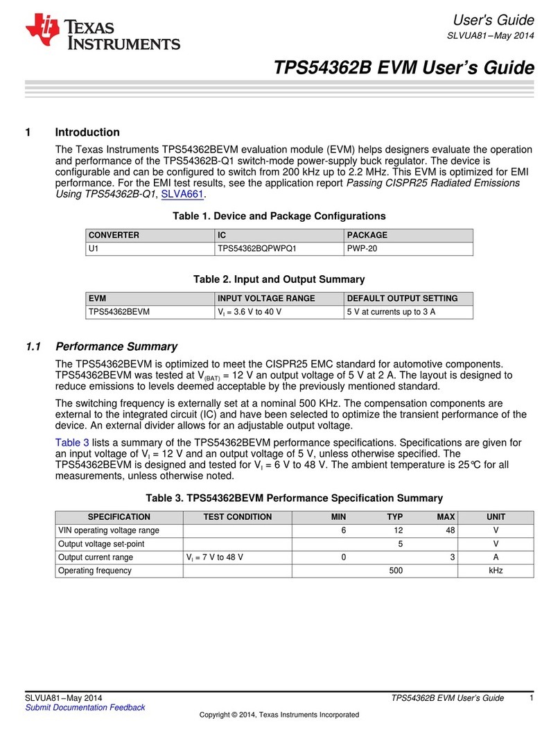
Texas Instruments TPS54362B EVM User manual
Texas Instruments
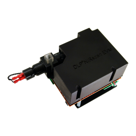
Texas Instruments DLP NIRscan EVM User manual
Texas Instruments
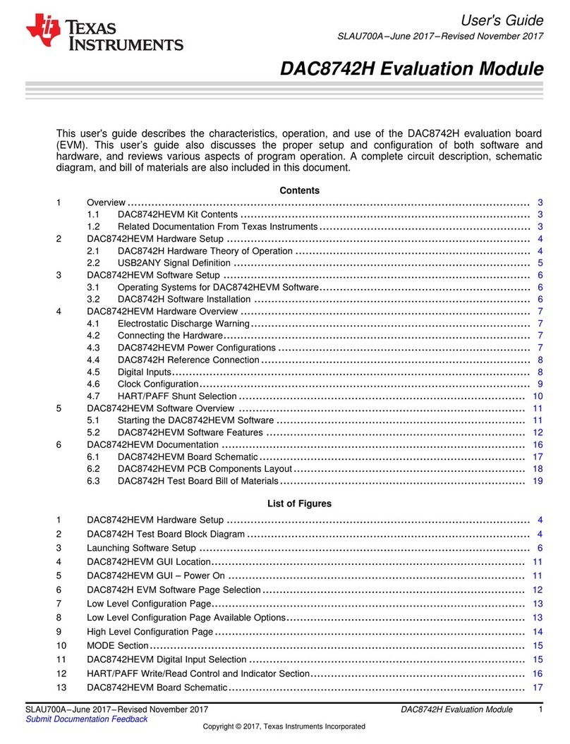
Texas Instruments DAC8742H User manual
Texas Instruments
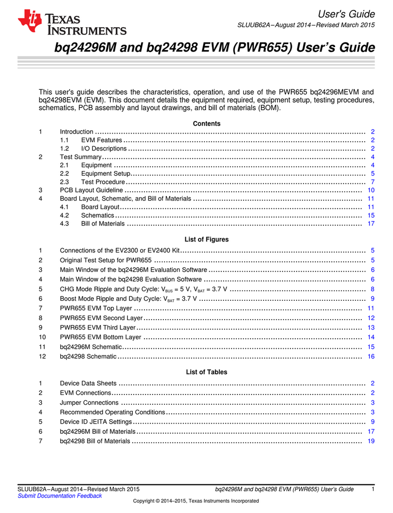
Texas Instruments BQ24296M User manual
Texas Instruments
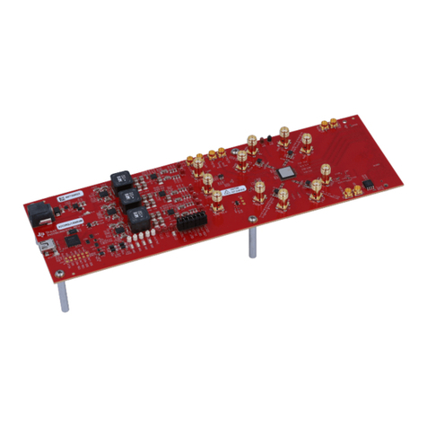
Texas Instruments ADC12DJ5200RF User manual
Texas Instruments
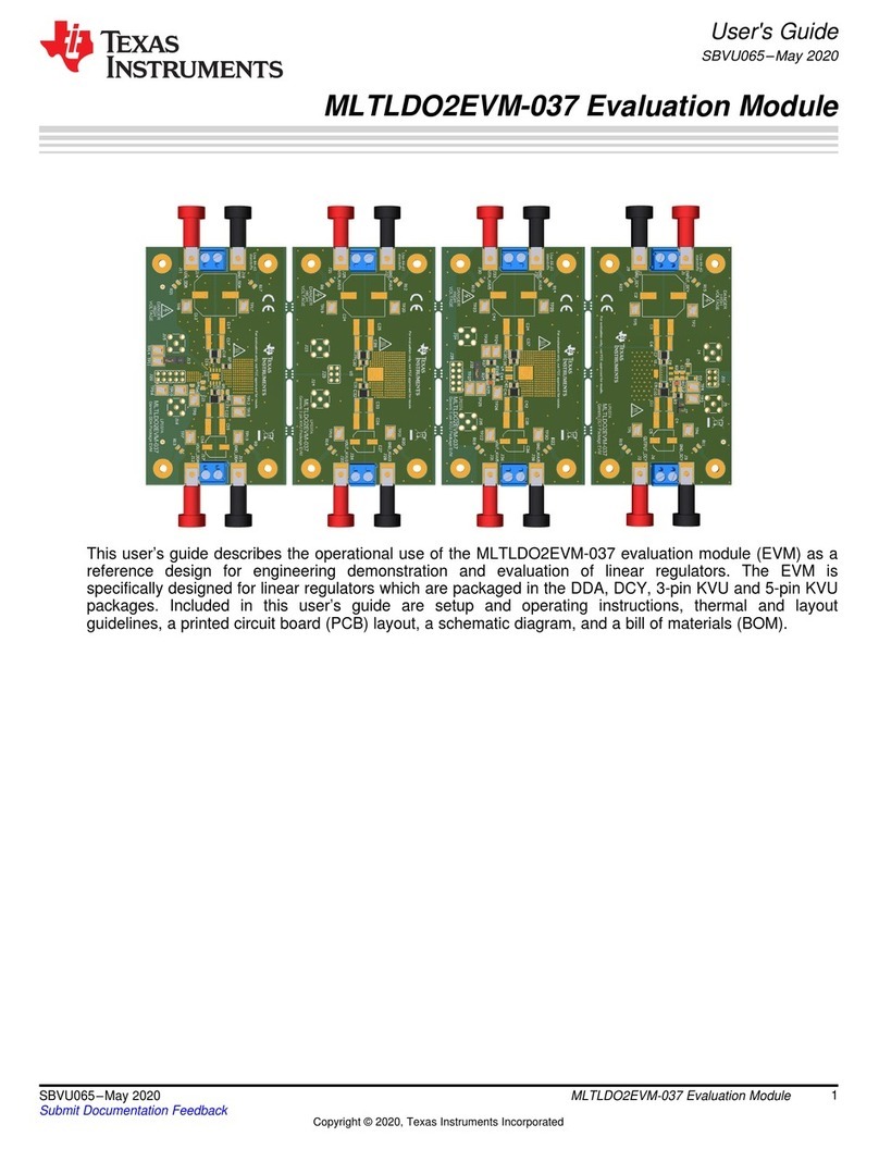
Texas Instruments MLTLDO2EVM-037 User manual
Texas Instruments
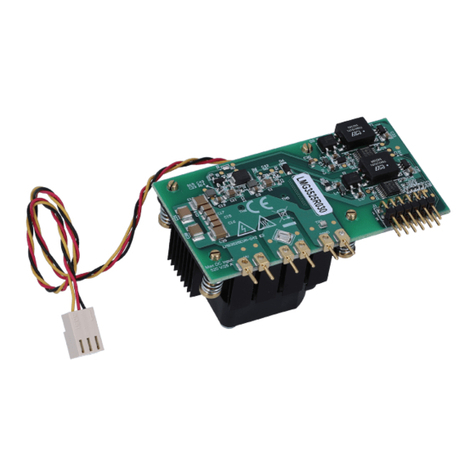
Texas Instruments LMG352 EVM-04 Series User manual
Texas Instruments
Texas Instruments TRF7963A User manual
Texas Instruments
Texas Instruments TPA6100A2 User manual
Texas Instruments
Texas Instruments TWL6032 User manual
Texas Instruments
Texas Instruments TPS25200EVM-618 User manual
Texas Instruments
Texas Instruments TLC5540 User manual
Texas Instruments
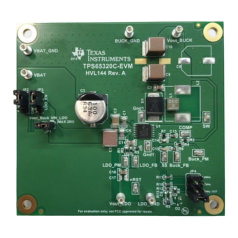
Texas Instruments TPS65320C-Q1-EVM User manual
Texas Instruments
Texas Instruments LMH9235RRL-EVM User manual
Popular Control Unit manuals by other brands
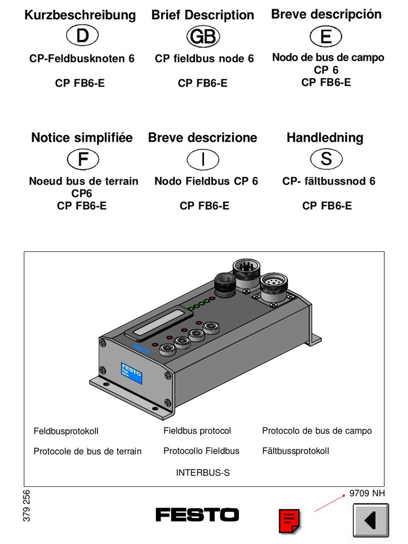
Festo
Festo Compact Performance CP-FB6-E Brief description
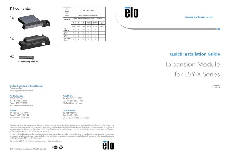
Elo TouchSystems
Elo TouchSystems DMS-SA19P-EXTME Quick installation guide
JS Automation
JS Automation MPC3034A user manual
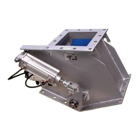
JAUDT
JAUDT SW GII 6406 Series Translation of the original operating instructions
Spektrum
Spektrum Air Module System manual
BOC Edwards
BOC Edwards Q Series instruction manual

KHADAS
KHADAS BT Magic quick start

Etherma
Etherma eNEXHO-IL Assembly and operating instructions
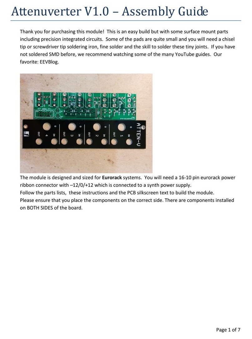
PMFoundations
PMFoundations Attenuverter Assembly guide
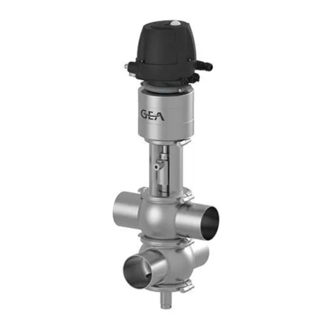
GEA
GEA VARIVENT Operating instruction
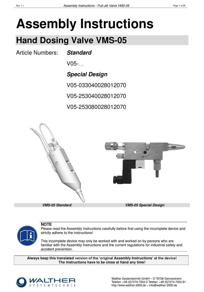
Walther Systemtechnik
Walther Systemtechnik VMS-05 Assembly instructions
Altronix
Altronix LINQ8PD Installation and programming manual
