2Common features and parameters
This section describes the features that are in common to the three boards, such as: UVLO, floating ground
configuration, current limitation, analog and digital telemetries, and explains how to customize them by changing
the external components on the board.
2.1 Undervoltage lockout and hysteresis settings
The UVLO and hysteresis can be programmed by a set of three resistors: the RHYS, RUVLO and RV.
A 220 kΩ resistor is generally used for RV, the other two resistors are obtained by the following equations:
RUVLO =2.5*RV
VTH_ON −2.5 − K (1)
RUVLO =2.5*RV
VTH_OFF −2.5 − RUVLO (2)
Where K=150 is a corrective fixed value to be added to Eq. (1) in order to take into account that during the rising
phase of supply voltage, in the UVLO external resistor divider, RHYS is shorted by a non-ideal switch embedded in
the RHRPMICL1A.
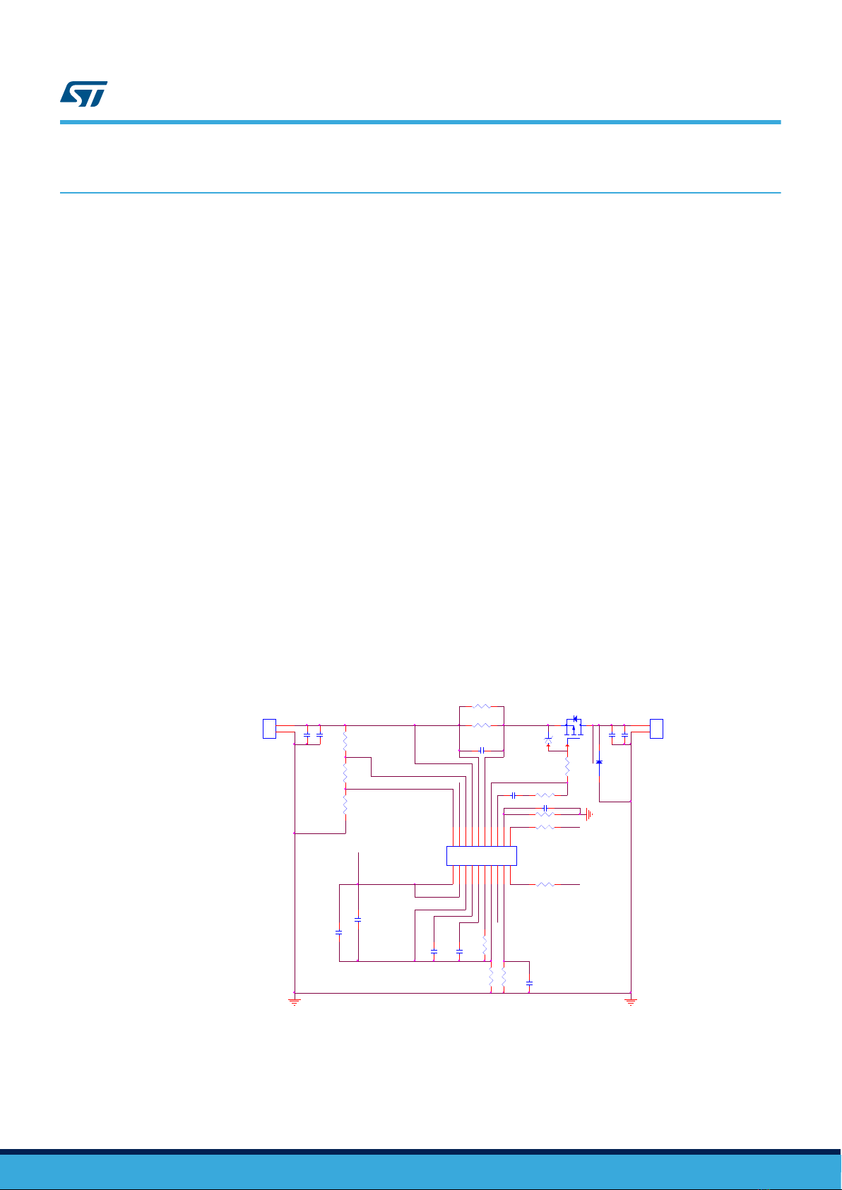
2.2 Gate driving
The driver circuit is designed to drive an external P-channel power MOSFET (connected in high-side
configuration) providing on the Vg pin a voltage signal in the range VCC down to (VCC - 12 V). All the evaluation
boards are equipped with a through-hole socket where the power MOSFET can be easily housed.
When the device is ON and no current limitation is active, the Vg node is pulled down and the gate of the external
MOSFET is internally clamped, about 12 V below the supply voltage VCC. When the MOSFET has to be switched
OFF, Vg is brought up to VCC.
When the MOSFET is in current limitation mode, the Vg voltage is a value inside the range [VCC-12 V, VCC],
defined by the limitation control loop.
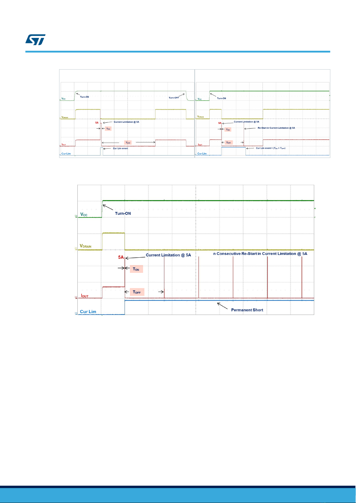
2.3 Current sense and limitation function
The voltage drop on the external RSENSE resistor is continuously monitored (by ISNS+ and ISNS- pins) and
compared with a fixed 100 mV internally generated threshold.
The current limitation threshold can be externally set according to the application requirements by a suitable
choice of the RSENSE resistor.
In the re-triggerable and latched evaluation boards it is:
ILIM = 100mV/RSENSE (3)
If the voltage drop on RSENSE exceeds 100 mV means that the current demand is becoming excessive: an
internal timer starts counting the trip-off time TON and the device enters the current limitation mode. In such a
condition the limitation control loop is enabled in order to force Vg to the proper voltage level, limiting the current
to the load.
Please refer Section 5.1.2.2 Bill of material of the EVAL-RHRICL1AFV1 board for the current limitation settings
in the foldback mode evaluation board.
2.4 Floating ground configuration
The evaluation boards are equipped with the RGND floating resistance mounted between the GND pin of the ICL
(GND) and the system ground (MGND).
An embedded 14.8 V Zener diode chain allows the device to operate in floating ground configuration and protects
the ICL device as its internal voltage supply is clamped at VZ ~ 15 V (14.8 V typ).
According to the voltage value of the Bus supply and depending on the value of RGND, the device can work (or
not) in floating ground condition, as follows:
UM2605
Common features and parameters
UM2605 - Rev 1 page 3/27