TQ TQMaRZG2x User manual

TQMaRZG2x
User's Manual
TQMaRZG2x UM 0100
29.03.2021

User's Manual l TQMaRZG2x UM 0100 l © 2021, TQ-Systems GmbH Page I
TABLE OF CONTENTS
1. ABOUT THIS MANUAL................................................................................................................................................................................1
1.1 Copyright and license expenses.............................................................................................................................................................1
1.2 Registered trademarks...............................................................................................................................................................................1
1.3 Disclaimer......................................................................................................................................................................................................1
1.4 Imprint............................................................................................................................................................................................................1
1.5 Tips on safety................................................................................................................................................................................................2
1.6 Symbols and typographic conventions ...............................................................................................................................................2
1.7 Handling and ESD tips...............................................................................................................................................................................2
1.8 Naming of signals........................................................................................................................................................................................3
1.9 Further applicable documents / presumed knowledge.................................................................................................................3
2. BRIEF DESCRIPTION ....................................................................................................................................................................................4
2.1 Block diagram...............................................................................................................................................................................................4
2.2 Functions and characteristics..................................................................................................................................................................4
3. ELECTRONICS................................................................................................................................................................................................5
3.1 Interfaces to other systems and devices..............................................................................................................................................5
3.1.1 Pin multiplexing...........................................................................................................................................................................................5
3.1.2 Impedances...................................................................................................................................................................................................5
3.1.3 Track length ..................................................................................................................................................................................................5
3.1.4 Pinout TQMaRZG2x ....................................................................................................................................................................................6
3.2 Boot source................................................................................................................................................................................................ 10
3.3 System components................................................................................................................................................................................ 12
3.3.1 RZ/G2x......................................................................................................................................................................................................... 12
3.3.1.1 RZ/G2x variants, block diagrams......................................................................................................................................................... 12
3.3.1.2 RZ/G2x variants, details.......................................................................................................................................................................... 13
3.3.2 Memory ....................................................................................................................................................................................................... 14
3.3.2.1 SDRAM......................................................................................................................................................................................................... 14
3.3.2.2 eMMC........................................................................................................................................................................................................... 14
3.3.2.3 QSPI NOR..................................................................................................................................................................................................... 14
3.3.2.4 EEPROM....................................................................................................................................................................................................... 15
3.3.2.5 EEPROM 24LC64T..................................................................................................................................................................................... 15
3.3.2.6 EEPROM SE97BTP..................................................................................................................................................................................... 15
3.3.3 RTC................................................................................................................................................................................................................ 16
3.3.4 Temperature sensor SE97BTP............................................................................................................................................................... 16
3.3.5 Secure Element SE050 ............................................................................................................................................................................ 17
3.4 Data interfaces .......................................................................................................................................................................................... 18
3.4.1 Audio............................................................................................................................................................................................................ 18
3.4.2 CAN............................................................................................................................................................................................................... 18
3.4.3 Clock............................................................................................................................................................................................................. 18
3.4.4 Display interfaces..................................................................................................................................................................................... 19
3.4.4.1 24-bit RGB................................................................................................................................................................................................... 19
3.4.4.2 HDMI ............................................................................................................................................................................................................ 20
3.4.4.3 LVDS ............................................................................................................................................................................................................. 20
3.4.5 CSI ................................................................................................................................................................................................................. 21
3.4.6 Ethernet....................................................................................................................................................................................................... 21
3.4.7 GPIO.............................................................................................................................................................................................................. 22
3.4.8 I2C.................................................................................................................................................................................................................. 23
3.4.9 Interrupt Controller ................................................................................................................................................................................. 23
3.4.10 JTAG®........................................................................................................................................................................................................... 24
3.4.11 MLB ............................................................................................................................................................................................................... 24
3.4.12 PCIe / SATA................................................................................................................................................................................................. 25
3.4.13 PWM ............................................................................................................................................................................................................. 25
3.4.14 SD / MMC Interface.................................................................................................................................................................................. 26
3.4.15 SPI (MSIOF)................................................................................................................................................................................................. 26
3.4.16 UART (SCIF / HSCIF).................................................................................................................................................................................. 27
3.4.17 USB................................................................................................................................................................................................................ 27

User's Manual l TQMaRZG2x UM 0100 l © 2021, TQ-Systems GmbH Page II
TABLE OF CONTENTS (continued)
3.5 Power........................................................................................................................................................................................................... 28
3.5.1 TQMaRZG2x supply................................................................................................................................................................................. 28
3.5.2 Power consumption TQMaRZG2x....................................................................................................................................................... 28
3.5.3 Power consumption RTC........................................................................................................................................................................ 29
3.5.4 Power supply outputs............................................................................................................................................................................. 29
3.5.5 Power modes............................................................................................................................................................................................. 30
3.6 Reset............................................................................................................................................................................................................. 31
3.7 Housekeeping........................................................................................................................................................................................... 32
3.7.1 Power sequencing ................................................................................................................................................................................... 32
3.7.2 Voltage monitoring................................................................................................................................................................................. 32
4. MECHANICS................................................................................................................................................................................................ 33
4.1 Assembly..................................................................................................................................................................................................... 33
4.2 Dimensions................................................................................................................................................................................................. 34
4.3 Weight ......................................................................................................................................................................................................... 36
4.4 Connectors................................................................................................................................................................................................. 36
4.5 Protection against external effects..................................................................................................................................................... 36
4.6 Thermal management............................................................................................................................................................................ 37
4.7 Structural requirements......................................................................................................................................................................... 37
4.8 Notes of treatment................................................................................................................................................................................... 37
5. SOFTWARE.................................................................................................................................................................................................. 37
6. SAFETY REQUIREMENTS AND PROTECTIVE REGULATIONS......................................................................................................... 38
6.1 EMC............................................................................................................................................................................................................... 38
6.2 ESD................................................................................................................................................................................................................ 38
6.3 Shock and Vibration ................................................................................................................................................................................ 38
6.4 Climatic and operational conditions.................................................................................................................................................. 39
6.5 Operational safety and personal security......................................................................................................................................... 39
6.6 Reliability and service life....................................................................................................................................................................... 39
7. ENVIRONMENT PROTECTION................................................................................................................................................................ 40
7.1 RoHS............................................................................................................................................................................................................. 40
7.2 WEEE®.......................................................................................................................................................................................................... 40
7.3 REACH®........................................................................................................................................................................................................ 40
7.4 EuP................................................................................................................................................................................................................ 40
7.5 Battery.......................................................................................................................................................................................................... 40
7.6 Packaging ................................................................................................................................................................................................... 40
7.7 Other entries.............................................................................................................................................................................................. 40
8. APPENDIX ................................................................................................................................................................................................... 41
8.1 Acronyms and definitions...................................................................................................................................................................... 41
8.2 References.................................................................................................................................................................................................. 43

User's Manual l TQMaRZG2x UM 0100 l © 2021, TQ-Systems GmbH Page III
TABLE DIRECTORY
Table 1: Terms and Conventions............................................................................................................................................................................2
Table 2: Impedances...................................................................................................................................................................................................5
Table 3: Track lengths ................................................................................................................................................................................................5
Table 4: Pinout connector X1...................................................................................................................................................................................6
Table 5: Pinout connector X2...................................................................................................................................................................................8
Table 6: Boot source selection.............................................................................................................................................................................. 10
Table 7: General boot settings.............................................................................................................................................................................. 11
Table 8: RZ/G2x variants......................................................................................................................................................................................... 13
Table 9: eMMC transfer modes............................................................................................................................................................................. 14
Table 10: EEPROM, TQMaRZG2x-specific data................................................................................................................................................... 15
Table 11: Temperature sensor SE97BTP............................................................................................................................................................... 16
Table 12: TQMaRZG2x Reset- and Status signals.............................................................................................................................................. 17
Table 13: Audio signals ............................................................................................................................................................................................. 18
Table 14: CAN signals................................................................................................................................................................................................. 18
Table 15: Clock signals .............................................................................................................................................................................................. 18
Table 16: 24-bit RGB signals..................................................................................................................................................................................... 19
Table 17: HDMI signals.............................................................................................................................................................................................. 20
Table 18: LVDS signals............................................................................................................................................................................................... 20
Table 19: CSI signals................................................................................................................................................................................................... 21
Table 20: Ethernet signals........................................................................................................................................................................................ 21
Table 21: GPIOs............................................................................................................................................................................................................ 22
Table 22: I2C1 device addresses............................................................................................................................................................................. 23
Table 23: I2C signals.................................................................................................................................................................................................... 23
Table 24: JTAG signals............................................................................................................................................................................................... 24
Table 25: MLB signals................................................................................................................................................................................................. 24
Table 26: PCIe / SATA signals................................................................................................................................................................................... 25
Table 27: PWM signals............................................................................................................................................................................................... 25
Table 28: SDHI signals................................................................................................................................................................................................ 26
Table 29: SPI signals ................................................................................................................................................................................................... 26
Table 30: UART signals .............................................................................................................................................................................................. 27
Table 31: USB signals................................................................................................................................................................................................. 27
Table 32: TQMaRZG2x supply inputs.................................................................................................................................................................... 28
Table 33: TQMaRZG2x current consumption..................................................................................................................................................... 28
Table 34: RTC power consumption....................................................................................................................................................................... 29
Table 35: TQMaRZG2x supply outputs................................................................................................................................................................. 29
Table 36: RZ/G2x Power Modes.............................................................................................................................................................................. 30
Table 37: TQMaRZG2x Power Modes details...................................................................................................................................................... 30
Table 38: Labels on TQMaRZG2x............................................................................................................................................................................ 33
Table 39: TQMaRZG2x heights................................................................................................................................................................................ 34
Table 40: Carrier board mating connectors........................................................................................................................................................ 36
Table 41: Shock resistance....................................................................................................................................................................................... 38
Table 42: Vibration resistance................................................................................................................................................................................. 38
Table 43: Climate and operational conditions................................................................................................................................................... 39
Table 44: Acronyms.................................................................................................................................................................................................... 41
Table 45: Further applicable documents............................................................................................................................................................. 43

User's Manual l TQMaRZG2x UM 0100 l © 2021, TQ-Systems GmbH Page IV
ILLUSTRATION DIRECTORY
Figure 1: Block diagram TQMaRZG2x (simplified)...............................................................................................................................................4
Figure 2: Block diagram boot strapping.............................................................................................................................................................. 10
Figure 3: Block diagram RZ/G2H............................................................................................................................................................................ 12
Figure 4: Block diagram RZ/G2M........................................................................................................................................................................... 12
Figure 5: Block diagram RZ/G2N............................................................................................................................................................................ 13
Figure 6: Block diagram eMMC interface............................................................................................................................................................ 14
Figure 7: Block diagram EEPROMs ........................................................................................................................................................................ 15
Figure 8: Block diagram RTC buffering................................................................................................................................................................ 16
Figure 9: Block diagram SE050............................................................................................................................................................................... 17
Figure 10: Block diagram I2C bus ............................................................................................................................................................................. 23
Figure 11: Block diagram JTAG................................................................................................................................................................................. 24
Figure 12: Block diagram Reset structure ............................................................................................................................................................. 31
Figure 13: Block diagram Housekeeping .............................................................................................................................................................. 32
Figure 14: TQMaRZG2x assembly, top ................................................................................................................................................................... 33
Figure 15: TQMaRZG2x assembly, bottom ........................................................................................................................................................... 33
Figure 16: TQMaRZG2x dimensions, side view.................................................................................................................................................... 34
Figure 17: TQMaRZG2x, dimensions, top through view................................................................................................................................... 34
Figure 18: Dimensions TQMaRZG2H ...................................................................................................................................................................... 35
Figure 19: Dimensions TQMaRZG2M, TQMaRZG2N .......................................................................................................................................... 35

User's Manual l TQMaRZG2x UM 0100 l © 2021, TQ-Systems GmbH Page V
REVISION HISTORY
Rev. Date Name Pos. Modification
0100 29.03.2021 Petz First edition

User's Manual l TQMaRZG2x UM 0100 l © 2021, TQ-Systems GmbH Page 1
1. ABOUT THIS MANUAL
1.1 Copyright and license expenses
Copyright protected © 2021 by TQ-Systems GmbH.
This User's Manual may not be copied, reproduced, translated, changed or distributed, completely or partially
in electronic, machine readable, or in any other form without the written consent of TQ-Systems GmbH.
The drivers and utilities for the components used as well as the BIOS are subject to the copyrights of the respective
manufacturers. The licence conditions of the respective manufacturer are to be adhered to.
Bootloader-licence expenses are paid by TQ-Systems GmbH and are included in the price.
Licence expenses for the operating system and applications are not taken into consideration and must be calculated / declared
separately.
1.2 Registered trademarks
TQ-Systems GmbH aims to adhere to copyrights of all graphics and texts used in all publications, and strives to use original
or license-free graphics and texts.
All brand names and trademarks mentioned in this User's Manual, including those protected by a third party, unless specified
otherwise in writing, are subjected to the specifications of the current copyright laws and the proprietary laws of the present
registered proprietor without any limitation. One should conclude that brand and trademarks are rightly protected by a third
party.
1.3 Disclaimer
TQ-Systems GmbH does not guarantee that the information in this User's Manual is up-to-date, correct, complete or of good
quality. Nor does TQ-Systems GmbH assume guarantee for further usage of the information. Liability claims against TQ-Systems
GmbH, referring to material or non-material related damages caused, due to usage or non-usage of the information given in this
User's Manual, or due to usage of erroneous or incomplete information, are exempted, as long as there is no proven intentional
or negligent fault of TQ-Systems GmbH.
TQ-Systems GmbH explicitly reserves the rights to change or add to the contents of this User's Manual or parts of it without
special notification.
Important Notice:
Before using the Starterkit MBaRZG2x or parts of the schematics of the MBaRZG2x, you must evaluate it and determine if it is
suitable for your intended application. You assume all risks and liability associated with such use. TQ-Systems GmbH makes no
other warranties including, but not limited to, any implied warranty of merchantability or fitness for a particular purpose. Except
where prohibited by law, TQ-Systems GmbH will not be liable for any indirect, special, incidental or consequential loss or damage
arising from the usage of the Starterkit MBaRZG2x or schematics used, regardless of the legal theory asserted.
1.4 Imprint
TQ-Systems GmbH
Gut Delling, Mühlstraße 2
D-82229 Seefeld
Tel: +49 8153 9308–0
Fax: +49 8153 9308–4223
E-Mail: Info@TQ-Group
Web: TQ-Group

User's Manual l TQMaRZG2x UM 0100 l © 2021, TQ-Systems GmbH Page 2
1.5 Tips on safety
Improper or incorrect handling of the product can substantially reduce its life span.
1.6 Symbols and typographic conventions
Table 1: Terms and Conventions
Symbol Meaning
This symbol represents the handling of electrostatic-sensitive modules and / or components. These
components are often damaged / destroyed by the transmission of a voltage higher than about 50 V.
A human body usually only experiences electrostatic discharges above approximately 3,000 V.
This symbol indicates the possible use of voltages higher than 24 V.
Please note the relevant statutory regulations in this regard.
Non-compliance with these regulations can lead to serious damage to your health and also cause
damage / destruction of the component.
This symbol indicates a possible source of danger. Acting against the procedure described can lead
to possible damage to your health and / or cause damage / destruction of the material used.
This symbol represents important details or aspects for working with TQ-products.
Command
A font with fixed-width is used to denote commands, contents, file names, or menu items.
1.7 Handling and ESD tips
General handling of your TQ-products
The TQ-product may only be used and serviced by certified personnel who have taken note of the
information, the safety regulations in this document and all related rules and regulations.
A general rule is, not to touch the TQ-product during operation. This is especially important when
switching on, changing jumper settings or connecting other devices without ensuring beforehand
that the power supply of the system has been switched off.
Violation of this guideline may result in damage / destruction of the TQMaRZG2x and be dangerous
to your health.
Improper handling of your TQ-product would render the guarantee invalid.
Proper ESD handling
The electronic components of your TQ-product are sensitive to electrostatic discharge (ESD).
Always wear antistatic clothing, use ESD-safe tools, packing materials etc., and operate your TQ-
product in an ESD-safe environment. Especially when you switch modules on, change jumper settings,
or connect other devices.

User's Manual l TQMaRZG2x UM 0100 l © 2021, TQ-Systems GmbH Page 3
1.8 Naming of signals
A hash mark (#) at the end of the signal name indicates a low-active signal.
Example: RESET#
If a signal can switch between two functions and if this is noted in the name of the signal, the low-active function is marked with
a hash mark and shown at the end.
Example: C / D#
If a signal has multiple functions, the individual functions are separated by slashes when they are important for the wiring.
The identification of the individual functions follows the above conventions.
Example: WE2# / OE#
1.9 Further applicable documents / presumed knowledge
•Specifications and manual of the modules used:
These documents describe the service, functionality and special characteristics of the module used (incl. BIOS).
•Specifications of the components used:
The manufacturer's specifications of the components used, for example CompactFlash cards, are to be taken note of.
They contain, if applicable, additional information that must be taken note of for safe and reliable operation.
These documents are stored at TQ-Systems GmbH.
•Chip errata:
It is the user's responsibility to make sure all errata published by the manufacturer of each component are taken note of.
The manufacturer’s advice should be followed.
•Software behaviour:
No warranty can be given, nor responsibility taken for any unexpected software behaviour due to deficient components.
•General expertise:
Expertise in electrical engineering / computer engineering is required for the installation and the use of the device.
The following documents are required to fully comprehend the following contents:
•MBaRZG2x circuit diagram
•MBaRZG2x User’s Manual
•RZ/G2x Data Sheet
•U-Boot documentation: www.denx.de/wiki/U-Boot/Documentation
•Yocto documentation: www.yoctoproject.org/docs/
•TQ-Support Wiki: TQMaRZG2x Support Wiki

User's Manual l TQMaRZG2x UM 0100 l © 2021, TQ-Systems GmbH Page 4
2. BRIEF DESCRIPTION
This User's Manual describes the hardware of the TQMaRZG2x as of revision 0100, and refers to some software settings.
A certain TQMaRZG2x derivative does not necessarily provide all features described in this User's Manual.
This User's Manual does also not replace the Renesas CPU Reference Manuals. The information provided in this User's Manual
is only valid in connection with the tailored boot loader, which is preinstalled on the TQMaRZG2x, and the BSP provided by TQ-
Systems; see also chapter 5.
The TQMaRZG2x is a universal Minimodule based on the Renesas CPUs RZ/G2H, RZ/G2M, or RZ/G2N. These CPUs feature up to
four Cortex®-A53 cores, up to four Cortex®-A57 cores and one Cortex®-R7 core.
The TQMaRZG2x extends the TQ-Systems GmbH product range and offers an outstanding computing performance.
All components required for the correct function of the CPU, like LPDDR4 SDRAM, eMMC, power supply and power management
are integrated on the TQMaRZG2x. All essential CPU pins are routed to the TQMaRZG2x connectors.
There are therefore no restrictions for customers using the TQMaRZG2x with respect to an integrated customised design.
The functionality of the different TQMaRZG2x is mainly determined by the features provided by the respective RZ/G2x derivative.
2.1 Block diagram
Temp. Sensor
RTC
EEPROM
System Controller
IO
Muxing
IO
Muxing
RZ/G2H
RZ/G2M
RZ/G2N
220-pin connector
LPDDR4 #1
(3200 MT/s) 32 bit + ECC
NOR Flash #1
(x1/x2/x4/x8)
NOR Flash #2
(x1/x2/x4)
eMMC
Power
Supply
Clock
LPDDR4 #2
(3200 MT/s)
TSE
220-pin connector
32 bit + ECC
Figure 1: Block diagram TQMaRZG2x (simplified)
2.2 Functions and characteristics
The TQMaRZG2x provides the following key functions and characteristics:
•CPU derivatives RZ/G2H, RZ/G2M, RZ/G2N
•Up to 8 Gbyte of LPDDR4 SDRAM, optional with In-Line ECC
•Up to 64 Gbyte of eMMC NAND flash (assembly option)
•Up to 512 Mbyte of QSPI NOR flash (assembly option)
•RTC (assembly option)
•64 Kbit EEPROM (assembly option)
•Secure Element SE050 (assembly option)
•Temperature sensor including EEPROM
•System Controller for reset control, power sequencing and power management, voltage supervision
•Voltage regulators and oscillators for all voltages and clocks used on the TQMaRZG2x
•All essential RZ/G2x signals routed to board-to-board connectors
•5 V single supply
•Dimensions of 77 mm × 50 mm

User's Manual l TQMaRZG2x UM 0100 l © 2021, TQ-Systems GmbH Page 5
3. ELECTRONICS
3.1 Interfaces to other systems and devices
3.1.1 Pin multiplexing
When using the processor signals the multiple pin configurations by different processor-internal function units must be taken
note of. The pin assignment in Table 4 and Table 5 refers to the BSP provided by TQ-Systems in combination with the MBaRZG2x.
Attention: Destruction or malfunction
Depending on the configuration many RZ/G2x pins can provide several different functions.
Please take note of the information concerning the configuration of these pins in (1), before
integration or start-up of your carrier board / Starterkit.
RFU: Reserved pins without function. To support future module revisions,
these pins must not be connected.
3.1.2 Impedances
By default, all signals have a single-ended impedance of nominal 50 Ω ±10 %. Depending on the interface, other impedances are
also used on the TQMaRZG2x. The following table shows the affected interfaces:
Table 2: Impedances
Interface Signal type Impedance TQMaRZG2x Recommendation for carrier board
CSI
Clock + data
100 Ω differential
100 Ω ±10 % differential
HDMI
Clock + data
100 Ω differential
100 Ω ±10 % differential
LVDS
Clock + data
100 Ω differential
100 Ω ±10 % differential
PCIe
Clock
100 Ω differential
100 Ω ±10 % differential
PCIe / SATA
Data
90 Ω differential
90 Ω ±10 % differential
USB 2.0
Data
90 Ω differential
90 Ω ±10 % differential
USB 3.0
Clock
100 Ω differential
100 Ω ±10 % differential
Data
90 Ω differential
90 Ω ±10 % differential
3.1.3 Track length
The following table shows the track lengths of critical TQMaRZG2x interfaces:
Table 3: Track lengths
Interface
Signal
RZ/G2x b
all to
TQMaRZG2x
connector [mm]
USB 3.0
RX
22.7
TX
23.2
CLK
19.8
PCIe0
RX
24.0
TX
24.9
CLK
28.6
PCIe1
RX
34.8
TX
36.4
CLK
42.4
LVDS
CH[3:0]
26.0
CLK
26.0
HDMI
DATA[2:0]
35.0
CLK
35.0
CSI0
DATA[3:0]
17.5
CLK
17.5
CSI1
DATA[3:0]
14.0
CLK
14.0

User's Manual l TQMaRZG2x UM 0100 l © 2021, TQ-Systems GmbH Page 6
3.1.4 Pinout TQMaRZG2x
Table 4: Pinout connector X1
Dir. Level Group Signal X1 Signal Group Level Dir.
–
0 V
Ground
DGND
A1
B1
DGND
Ground
0 V
–
I
5 V
Power
V_5V_IN
A2
B2
V_5V_IN
Power
5 V
I
I
5 V
Power
V_5V_IN
A3
B3
V_5V_IN
Power
5 V
I
I
5 V
Power
V_5V_IN
A4
B4
V_5V_IN
Power
5 V
I
I
5 V
Power
V_5V_IN
A5
B5
V_5V_IN
Power
5 V
I
I 5 V Power V_5V_IN A6 B6 V_5V_IN Power 5 V I
I
5 V
Power
V_5V_IN
A7
B7
V_5V_IN
Power
5 V
I
I
5 V
Power
V_5V_IN
A8
B8
V_5V_IN
Power
5 V
I
–
0 V
Ground
DGND
A9
B9
DGND
Ground
0 V
–
–
0 V
Ground
DGND
A10
B10
DGND
Ground
0 V
–
–
0 V
Ground
DGND
A11
B11
DGND
Ground
0 V
–
–
0 V
Ground
DGND
A12
B12
DGND
Ground
0 V
–
O
1.8 V
Power
V_1V8
A13
B13
V_3V3
Power
3.3 V
O
O
1.8 V
Power
V_1V8
A14
B14
V_3V3
Power
3.3 V
O
–
0 V
Ground
DGND
A15
B15
DGND
Ground
0 V
–
O
1.8 V
HDMI
HDMI0_TMDS_DATA2_P
A16
B16
HDMI0_TMDS_DATA1_P
HDMI
1.8 V
O
O
1.8 V
HDMI
HDMI0_TMDS_DATA2_N
A17
B17
HDMI0_TMDS_DATA1_N
HDMI
1.8 V
O
–
0 V
Ground
DGND
A18
B18
DGND
Ground
0 V
–
O
1.8 V
HDMI
HDMI0_TMDS_CLK_P
A19
B19
HDMI0_TMDS_DATA0_P
HDMI
1.8 V
O
O
1.8 V
HDMI
HDMI0_TMDS_CLK_N
A20
B20
HDMI0_TMDS_DATA0_N
HDMI
1.8 V
O
–
0 V
Ground
DGND
A21
B21
DGND
Ground
0 V
–
I 5 V HDMI HDMI0_HPD A22 B22 HDMI0_SCL HDMI 1.8 V O
IO
3.3 V
GPIO
GP7_02
A23
B23
HDMI0_SDA
HDMI
1.8 V
IO
–
0 V
Ground
DGND
A24
B24
DGND
Ground
0 V
–
O
1.8 V
LVDS
LVDS0_CH2_P
A25
B25
LVDS0_CH0_P
LVDS
1.8 V
O
O
1.8 V
LVDS
LVDS0_CH2_N
A26
B26
LVDS0_CH0_N
LVDS
1.8 V
O
–
0 V
Ground
DGND
A27
B27
DGND
Ground
0 V
–
O
1.8 V
LVDS
LVDS0_CH3_P
A28
B28
LVDS0_CH1_P
LVDS
1.8 V
O
O
1.8 V
LVDS
LVDS0_CH3_N
A29
B29
LVDS0_CH1_N
LVDS
1.8 V
O
–
0 V
Ground
DGND
A30
B30
DGND
Ground
0 V
–
–
0 V
Ground
DGND
A31
B31
DGND
Ground
0 V
–
I
1.8 V
CSI
CSI0_DATA0_P
A32
B32
LVDS0_CLK_P
LVDS
1.8 V
O
I
1.8 V
CSI
CSI0_DATA0_N
A33
B33
LVDS0_CLK_N
LVDS
1.8 V
O
–
0 V
Ground
DGND
A34
B34
DGND
Ground
0 V
–
I
1.8 V
CSI
CSI0_DATA2_P
A35
B35
CSI0_DATA1_P
CSI
1.8 V
I
I
1.8 V
CSI
CSI0_DATA2_N
A36
B36
CSI0_DATA1_N
CSI
1.8 V
I
–
0 V
Ground
DGND
A37
B37
DGND
Ground
0 V
–
I
1.8 V
CSI
CSI0_CLK_P
A38
B38
CSI0_DATA3_P
CSI
1.8 V
I
I
1.8 V
CSI
CSI0_CLK_N
A39
B39
CSI0_DATA3_N
CSI
1.8 V
I
–
0 V
Ground
DGND
A40
B40
DGND
Ground
0 V
–
–
0 V
Ground
DGND
A41
B41
DGND
Ground
0 V
–
I
1.8 V
CSI
CSI1_CLK_P
A42
B42
CSI1_DATA0_P
CSI
1.8 V
I
I
1.8 V
CSI
CSI1_CLK_N
A43
B43
CSI1_DATA0_N
CSI
1.8 V
I
–
0 V
Ground
DGND
A44
B44
DGND
Ground
0 V
–
I
1.8 V
DU
DU_DOT_CLK2_IN
A45
B45
CSI1_DATA1_P
CSI
1.8 V
I
–
0 V
Ground
DGND
A46
B46
CSI1_DATA1_N
CSI
1.8 V
I
I
1.8 V
DU
DU_DOT_CLK1_IN
A47
B47
DGND
Ground
0 V
–
–
0 V
Ground
DGND
A48
B48
SDA4
I2C
1.8 V
IO
I
1.8 V
DU
DU_DOT_CLK0_IN
A49
B49
SCL4
I2C
1.8 V
O
–
0 V
Ground
DGND
A50
B50
DGND
Ground
0 V
–
–
0 V
Ground
DGND
A51
B51
DGND
Ground
0 V
–
O
3.3 V
LBSC
CLKOUT
A52
B52
RD_WR#
LBSC
3.3 V
O
–
0 V
Ground
DGND
A53
B53
BS#
LBSC
3.3 V
O
IO
3.3 V
IIC_DVFS
IIC_DVFS_SDA
A54
B54
WE0#
LBSC
3.3 V
O
O
3.3 V
IIC_DVFS
IIC_DVFS_SCL
A55
B55
WE1#
LBSC
3.3 V
O

User's Manual l TQMaRZG2x UM 0100 l © 2021, TQ-Systems GmbH Page 7
3.1.4 Pinout TQMaRZG2x (continued)
Table 4: Pinout connector X1 (continued)
Dir. Level Group Signal X1 Signal Group Level Dir.
–
0 V
Ground
DGND
A56
B56
RD#
LBSC
3.3 V
O
O
3.3 V
GPIO
AVS1
A57
B57
CS1#
LBSC
3.3 V
O
O
3.3 V
GPIO
AVS2
A58
B58
CS0#
LBSC
3.3 V
O
IO
3.3 V
GPIO
GP7_03
A59
B59
EX_WAIT0_A
LBSC
3.3 V
I
–
0 V
Ground
DGND
A60
B60
DGND
Ground
0 V
–
O 3.3 V LBSC A0 A61 B61 D0 LBSC 3.3 V IO
O
3.3 V
LBSC
A1
A62
B62
D1
LBSC
3.3 V
IO
O
3.3 V
LBSC
A2
A63
B63
D2
LBSC
3.3 V
IO
O
3.3 V
LBSC
A3
A64
B64
D3
LBSC
3.3 V
IO
O
3.3 V
LBSC
A4
A65
B65
D4
LBSC
3.3 V
IO
O
3.3 V
LBSC
A5
A66
B66
D5
LBSC
3.3 V
IO
O
3.3 V
LBSC
A6
A67
B67
D6
LBSC
3.3 V
IO
O
3.3 V
LBSC
A7
A68
B68
D7
LBSC
3.3 V
IO
O
3.3 V
LBSC
A8
A69
B69
D8
LBSC
3.3 V
IO
–
0 V
Ground
DGND
A70
B70
DGND
Ground
0 V
–
O
3.3 V
LBSC
A9
A71
B71
D9
LBSC
3.3 V
IO
O
3.3 V
LBSC
A10
A72
B72
D10
LBSC
3.3 V
IO
O
3.3 V
LBSC
A11
A73
B73
D11
LBSC
3.3 V
IO
O
3.3 V
LBSC
A12
A74
B74
D12
LBSC
3.3 V
IO
O
3.3 V
LBSC
A13
A75
B75
D13
LBSC
3.3 V
IO
O
3.3 V
LBSC
A14
A76
B76
D14
LBSC
3.3 V
IO
O 3.3 V LBSC A15 A77 B77 D15 LBSC 3.3 V IO
O
3.3 V
LBSC
A16
A78
B78
DGND
Ground
0 V
–
O
3.3 V
LBSC
A17
A79
B79
IRQ0
INTC
3.3 V
I
–
0 V
Ground
DGND
A80
B80
DGND
Ground
0 V
–
O
3.3 V
LBSC
A18
A81
B81
IRQ1
INTC
3.3 V
I
O
3.3 V
LBSC
A19
A82
B82
IRQ2
INTC
3.3 V
I
–
0 V
Ground
DGND
A83
B83
IRQ3
INTC
3.3 V
I
I
3.3 V
INTC
IRQ5
A84
B84
IRQ4
INTC
3.3 V
I
O
3.3 V
PWM
PWM
A85
B85
DGND
Ground
0 V
–
O
3.3 V
PWM
PWM1_A
A86
B86
AVB_TXCREFCLK
EtherAVB
3.3 V
I
O
3.3 V
PWM
PWM2_A
A87
B87
DGND
Ground
0 V
–
–
0 V
Ground
DGND
A88
B88
AVB_TX_CTL
EtherAVB
2.5 V
O
I
2.5 V
EtherAVB
AVB_RXC
A89
B89
AVB_TXC
EtherAVB
2.5 V
O
–
0 V
Ground
DGND
A90
B90
DGND
Ground
0 V
–
I
2.5 V
EtherAVB
AVB_RX_CTL
A91
B91
AVB_TD0
EtherAVB
2.5 V
O
I
2.5 V
EtherAVB
AVB_RD0
A92
B92
AVB_TD1
EtherAVB
2.5 V
O
I
2.5 V
EtherAVB
AVB_RD1
A93
B93
AVB_TD2
EtherAVB
2.5 V
O
I
2.5 V
EtherAVB
AVB_RD2
A94
B94
AVB_TD3
EtherAVB
2.5 V
O
I
2.5 V
EtherAVB
AVB_RD3
A95
B95
DGND
Ground
0 V
–
–
0 V
Ground
DGND
A96
B96
AVB_MDIO
EtherAVB
3.3 V
IO
O
3.3 V
EtherAVB
AVB_MAGIC
A97
B97
AVB_MDC
EtherAVB
3.3 V
O
I
3.3 V
EtherAVB
AVB_PHY_INT
A98
B98
DGND
Ground
0 V
–
I
3.3 V
EtherAVB
AVB_LINK
A99
B99
RPC_INT#
RPC
1.8 V
I
–
0 V
Ground
DGND
A100
B100
DGND
Ground
0 V
–
O
3.3 V
EtherAVB
AVB_AVTP_MATCH_A
A101
B101
RPC_WP#
RPC
1.8 V
O
I
3.3 V
EtherAVB
AVB_AVTP_CAPTURE_A
A102
B102
RPC_RESET#
RPC
1.8 V
O
–
0 V
Ground
DGND
A103
B103
DGND
Ground
0 V
–
O
1.8 V
QSPI
QSPI1_CLK_CON
A104
B104
QSPI0_CLK_CON
QSPI
1.8 V
O
IO
1.8 V
QSPI
QSPI1_IO0_CON
A105
B105
QSPI0_IO0_CON
QSPI
1.8 V
IO
IO
1.8 V
QSPI
QSPI1_IO1_CON
A106
B106
QSPI0_IO1_CON
QSPI
1.8 V
IO
IO
1.8 V
QSPI
QSPI1_IO2_CON
A107
B107
QSPI0_IO2_CON
QSPI
1.8 V
IO
IO
1.8 V
QSPI
QSPI1_IO3_CON
A108
B108
QSPI0_IO3_CON
QSPI
1.8 V
IO
O
1.8 V
QSPI
QSPI1_SS#_CON
A109
B109
QSPI0_SS#_CON
QSPI
1.8 V
O
–
0 V
Ground
DGND
A110
B110
DGND
Ground
0 V
–

User's Manual l TQMaRZG2x UM 0100 l © 2021, TQ-Systems GmbH Page 8
3.1.4 Pinout TQMaRZG2x (continued)
Table 5: Pinout connector X2
Dir. Level Group Signal X2 Signal Group Level Dir.
–
0 V
Ground
DGND
A1
B1
DGND
Ground
0 V
–
I
0.8 V
PCIE
PCIE1_CLK_P
A2
B2
PCIE0_CLK_P
PCIE
0.8 V
I
I
0.8 V
PCIE
PCIE1_CLK_M
A3
B3
PCIE0_CLK_M
PCIE
0.8 V
I
–
0 V
Ground
DGND
A4
B4
DGND
Ground
0 V
–
O
0.8 V
PCIE
PCIE1_TX_P
A5
B5
PCIE0_TX_P
PCIE
0.8 V
O
O 0.8 V PCIE PCIE1_TX_M A6 B6 PCIE0_TX_M PCIE 0.8 V O
–
0 V
Ground
DGND
A7
B7
DGND
Ground
0 V
–
I
0.8 V
PCIE
PCIE1_RX_P
A8
B8
PCIE0_RX_P
PCIE
0.8 V
I
I
0.8 V
PCIE
PCIE1_RX_M
A9
B9
PCIE0_RX_M
PCIE
0.8 V
I
–
0 V
Ground
DGND
A10
B10
DGND
Ground
0 V
–
–
0 V
Ground
DGND
A11
B11
DGND
Ground
0 V
–
O
0.8 V
USB 3.0
USB3S0_TX_P
A12
B12
USB3HS0_DP
USB 3.0
3.3 V
IO
O
0.8 V
USB 3.0
USB3S0_TX_M
A13
B13
USB3HS0_DM
USB 3.0
3.3 V
IO
–
0 V
Ground
DGND
A14
B14
DGND
Ground
0 V
–
I
0.8 V
USB 3.0
USB3S0_RX_P
A15
B15
USB3S0_CLK_P
USB 3.0
0.8 V
I
I
0.8 V
USB 3.0
USB3S0_RX_M
A16
B16
USB3S0_CLK_M
USB 3.0
0.8 V
I
–
0 V
Ground
DGND
A17
B17
DGND
Ground
0 V
–
IO
3.3 V
USB 2.0
DP1
A18
B18
DP0
USB 2.0
3.3 V
IO
IO
3.3 V
USB 2.0
DM1
A19
B19
DM0
USB 2.0
3.3 V
IO
–
0 V
Ground
DGND
A20
B20
DGND
Ground
0 V
–
–
0 V
Ground
DGND
A21
B21
DGND
Ground
0 V
–
I 3.3 V USB 2.0 ID1 A22 B22 VBUS0 USB 2.0 5 V I
O
3.3 V
USB 2.0
USB1_PWEN
A23
B23
ID0
USB 2.0
3.3 V
I
I
3.3 V
USB 2.0
USB1_OVC
A24
B24
USB0_PWREN
USB 2.0
3.3 V
O
I
5 V
USB 3.0
USB3HS0_VBUS
A25
B25
USB0_OVC
USB 2.0
3.3 V
I
I
3.3 V
USB 3.0
USB3HS0_ID
A26
B26
DGND
Ground
0 V
–
O
3.3 V
USB 3.0
USB30_PWEN
A27
B27
SD3_DAT3_CON
SD
1.8 / 3.3 V
IO
I
3.3 V
USB 3.0
USB30_OVC
A28
B28
SD3_DAT2_CON
SD
1.8 / 3.3 V
IO
–
0 V
Ground
DGND
A29
B29
SD3_DAT1_CON
SD
1.8 / 3.3 V
IO
O
1.8 / 3.3 V
SD
SD3_CLK_CON
A30
B30
SD3_DAT0_CON
SD
1.8 / 3.3 V
IO
–
0 V
Ground
DGND
A31
B31
DGND
Ground
0 V
–
IO
1.8 / 3.3 V
SD
SD3_DAT7_CON
A32
B32
SD3_DS_CON
SD
1.8 / 3.3 V
I
IO
1.8 / 3.3 V
SD
SD3_DAT6_CON
A33
B33
SD3_CMD_CON
SD
1.8 / 3.3 V
IO
IO
1.8 / 3.3 V
SD
SD3_DAT5_CON
A34
B34
RTC_INT_OUT#
RTC
3.3 V
O
IO
1.8 / 3.3 V
SD
SD3_DAT4_CON
A35
B35
DGND
Ground
0 V
–
–
0 V
Ground
DGND
A36
B36
TRST#
DBG
1.8 V
I
I
3.3 V
RTC
V_BAT
A37
B37
TDI
DBG
1.8 V
I
–
0 V
Ground
DGND
A38
B38
TMS
DBG
1.8 V
I
I
3.3 V
SYSC
SWD_CLK
A39
B39
ASEBRK
DBG
1.8 V
IO
IO
3.3 V
SYSC
SWD_DIO
A40
B40
TDO
DBG
1.8 V
O
–
0 V
Ground
DGND
A41
B41
DGND
Ground
0 V
–
O
3.3 V
RESET
TQMARZG_RST_OUT#
A42
B42
TCK
DBG
1.8 V
I
I
3.3 V
RESET
TQMARZG_RST_IN#
A43
B43
JTAG_SRST#
SYSC
3.3 V
I
–
0 V
Ground
DGND
A44
B44
DGND
Ground
0 V
–
O
3.3 V
SYSC
PGOOD
A45
B45
USB_EXTAL_CON
USB
1.8 V
I
O
3.3 V
SYSC
BOOT_CFG#
A46
B46
DGND
Ground
0 V
–
–
–
RESERVED
RFU0
A47
B47
SYSC_UART0_TX
SYSC
3.3 V
O
–
–
RESERVED
RFU1
A48
B48
SYSC_UART0_RX
SYSC
3.3 V
I
–
–
RESERVED
RFU2
A49
B49
DGND
Ground
0 V
–
I
1.8 V
INTC
NMI
A50
B50
EXTALR_CON
CPG
1.8 V
I
–
0 V
Ground
DGND
A51
B51
DGND
Ground
0 V
–
IO
3.3 V
GPIO
GP6_30
A52
B52
FSCLKST#
CPG
1.8 V
O
IO
3.3 V
GPIO
GP6_31
A53
B53
DGND
Ground
0 V
–
–
0 V
Ground
DGND
A54
B54
AUDIO_CLKB_B
ADG
3.3 V
I
IO
3.3 V
SSI
SSI_SDATA9_A
A55
B55
DGND
Ground
0 V
–

User's Manual l TQMaRZG2x UM 0100 l © 2021, TQ-Systems GmbH Page 9
3.1.4 Pinout TQMaRZG2x (continued)
Table 5: Pinout connector X2 (continued)
Dir. Level Group Signal X2 Signal Group Level Dir.
IO
3.3 V
SSI
SSI_SDATA8
A56
B56
AUDIO_CLKA_A
ADG
3.3 V
I
IO
3.3 V
SSI
SSI_SDATA7
A57
B57
DGND
Ground
0 V
–
IO
3.3 V
SSI
SSI_SDATA6
A58
B58
SSI_SCK5
SSI
3.3 V
IO
IO
3.3 V
SSI
SSI_SDATA5
A59
B59
DGND
Ground
0 V
–
–
0 V
Ground
DGND
A60
B60
DGND
Ground
0 V
–
IO 3.3 V SSI SSI_SDATA4 A61 B61 SSI_SCK6 SSI 3.3 V IO
IO
3.3 V
SSI
SSI_SDATA3
A62
B62
DGND
Ground
0 V
–
IO
3.3 V
SSI
SSI_SDATA2_A
A63
B63
SSI_SCK78
SSI
3.3 V
IO
IO
3.3 V
SSI
SSI_SDATA1_A
A64
B64
DGND
Ground
0 V
–
IO
3.3 V
SSI
SSI_SDATA0
A65
B65
SSI_SCK4
SSI
3.3 V
IO
IO
3.3 V
SSI
SSI_WS78
A66
B66
DGND
Ground
0 V
–
IO
3.3 V
SSI
SSI_WS5
A67
B67
SSI_SCK349
SSI
3.3 V
IO
IO
3.3 V
SSI
SSI_WS6
A68
B68
DGND
Ground
0 V
–
IO
3.3 V
SSI
SSI_WS4
A69
B69
SSI_SCK01239
SSI
3.3 V
IO
–
0 V
Ground
DGND
A70
B70
DGND
Ground
0 V
–
IO
3.3 V
SSI
SSI_WS349
A71
B71
VDDQVA_SD0
SD
1.8 / 3.3 V
I
IO
3.3 V
SSI
SSI_WS01239
A72
B72
VDDQVA_SD1
SD
1.8 / 3.3 V
I
O
3.3 V
TEMP
EVENT_TEMPSENSOR#
A73
B73
VDDQVA_SD2
SD
1.8 / 3.3 V
I
I
3.3 V
EEPROM
EEPROM_WP
A74
B74
VDDQVA_SD3
SD
1.8 / 3.3 V
I
O
3.3 V
SCIF
TX0
A75
B75
DGND
Ground
0 V
–
I
3.3 V
SCIF
RX0
A76
B76
SCK2
SCIF
3.3 V
O
IO 3.3 V SCIF CTS0# A77 B77 DGND Ground 0 V –
IO
3.3 V
SCIF
RTS0#
A78
B78
TX2_A
SCIF
3.3 V
O
O
3.3 V
SCIF
SCK0
A79
B79
RX2_A
SCIF
3.3 V
I
–
0 V
Ground
DGND
A80
B80
DGND
Ground
0 V
–
O
3.3 V
SCIF
TX1_A
A81
B81
MLB_CLK
MLB
3.3 V
I
I
3.3 V
SCIF
RX1_A
A82
B82
MLB_DAT
MLB
3.3 V
IO
IO
3.3 V
SCIF
CTS1#
A83
B83
MLB_SIG
MLB
3.3 V
IO
IO
3.3 V
SCIF
RTS1#
A84
B84
HRTS0#
HSCIF
3.3 V
IO
IO
3.3 V
MSIOF
MSIOF0_SYNC
A85
B85
HCTS0#
HSCIF
3.3 V
IO
O
3.3 V
MSIOF
MSIOF0_TXD
A86
B86
HRX0
HSCIF
3.3 V
I
I
3.3 V
MSIOF
MSIOF0_RXD
A87
B87
HTX0
HSCIF
3.3 V
O
O
3.3 V
MSIOF
MSIOF0_SS1
A88
B88
DGND
Ground
0 V
–
O
3.3 V
MSIOF
MSIOF0_SS2
A89
B89
HSCK0
HSCIF
3.3 V
I
–
0 V
Ground
DGND
A90
B90
DGND
Ground
0 V
–
O
3.3 V
MSIOF
MSIOF0_SCK
A91
B91
SD1_DAT0
SD
1.8 / 3.3 V
IO
–
0 V
Ground
DGND
A92
B92
SD1_DAT1
SD
1.8 / 3.3 V
IO
I
3.3 V
SD
SD0_WP
A93
B93
SD1_DAT2
SD
1.8 / 3.3 V
IO
I
3.3 V
SD
SD0_CD
A94
B94
SD1_DAT3
SD
1.8 / 3.3 V
IO
IO
1.8 / 3.3 V
SD
SD0_CMD
A95
B95
SD1_CD
SD
3.3 V
I
IO
1.8 / 3.3 V
SD
SD0_DAT0
A96
B96
SD1_WP
SD
3.3 V
I
IO
1.8 / 3.3 V
SD
SD0_DAT1
A97
B97
SD1_CMD
SD
1.8 / 3.3 V
IO
IO
1.8 / 3.3 V
SD
SD0_DAT2
A98
B98
DGND
Ground
0 V
–
IO
1.8 / 3.3 V
SD
SD0_DAT3
A99
B99
SD1_CLK
SD
1.8 / 3.3 V
O
–
0 V
Ground
DGND
A100
B100
DGND
Ground
0 V
–
O
1.8 / 3.3 V
SD
SD0_CLK
A101
B101
DGND
Ground
0 V
–
–
0 V
Ground
DGND
A102
B102
SD2_DAT0
SD
1.8 / 3.3 V
IO
I
3.3 V
SECURE
SE_ENABLE
A103
B103
SD2_DAT1
SD
1.8 / 3.3 V
IO
IO
3.3 V
SECURE
SE_7816_IO1
A104
B104
SD2_DAT2
SD
1.8 / 3.3 V
IO
IO
3.3 V
SECURE
SE_7816_IO2
A105
B105
SD2_DAT3
SD
1.8 / 3.3 V
IO
I
3.3 V
SECURE
SE_7816_RST#
A106
B106
SD2_CMD
SD
1.8 / 3.3 V
IO
IO
3.3 V
SECURE
SE_14443_LA
A107
B107
SD2_DS
SD
1.8 / 3.3 V
I
IO
3.3 V
SECURE
SE_14443_LB
A108
B108
DGND
Ground
0 V
–
O
3.3 V
SECURE
SE_7816_CLK
A109
B109
SD2_CLK
SD
1.8 / 3.3 V
O
–
0 V
Ground
DGND
A110
B110
DGND
Ground
0 V
–

User's Manual l TQMaRZG2x UM 0100 l © 2021, TQ-Systems GmbH Page 10
3.2 Boot source
The boot source is selected via the boot strapping pins of the RZ/G2x. All signals are routed to the TQMaRZG2x connectors.
After the release of PRESET# the configuration is read in. Depending on the boot device the RZ/G2x may read the data directly
from the boot device or the RZ/G2x boots from its on-chip boot ROM and loads the IPL into the internal RAM.
It is recommended to switch the boot strap pins to high impedance after read-in.
MDT[1:0]
RZ/G2x
Pin-Strapping
- Active driver during RESET#
- High-Z during normal operation
PORESET#
RST_IN#
System
Controller
MD[28:25]
MD[23:0]
BOOT_CFG#
Signal for
pin strapping driver
Connector
Figure 2: Block diagram boot strapping
Table 6: Boot source selection
X1-B67 X1-B66 X1-B64 X1-B63 Boot source Boot interface
MD4 MD3 MD2 MD1
0
1
0
0
NOR flash QSPI
1
1
0
1
eMMC SDHI3
1
1
1
0
USB download USB2_CH0
1
1
1
1
SCIF download SCIF2
Note: Field software updates
When designing a carrier board, it is recommended to include an interface
for software updates in the field.

User's Manual l TQMaRZG2x UM 0100 l © 2021, TQ-Systems GmbH Page 11
3.2 Boot source (continued)
Table 7: General boot settings
Boot config pin
TQMaRZG2x
Setting Remark
MDT1 X1-B56 JTAG section. More information in (1) and (2). Don’t care
MDT0 X1-B53
MD28 X1-A61 0 – RCLK from inside
1 – RCLK from EXTALR 1
MD27 X1-A62 00 – LPDDR4
Other settings are prohibited 00
MD22 X1-A68
MD26 X1-A64 Reserved, fixed to 0 0
MD25 X1-A65 Reserved, fixed to 0 0
MD23 X1-A67 Reserved, fixed to 0 0
MD21 X1-A74
JTAG section. More information in (1) and (2). Don’t care
MD20 X1-A72
MD11 X1-B65
MD10 X1-B75
MD19 X1-A75 00 – DDR3200
01 – DDR2800
10 – Setting prohibited
11 – DDR1600
00
MD17 X1-A77
MD18 X1-A76 0 – PLL1 division ratio: 1/24
1 – PLL1 division ratio: 1/36 0
MD16 X1-A78 Reserved, fixed to 1 1
MD15 X1-A79 0 – AArch32
1 – AArch64 0
MD14 X1-A81 EXTAL Select:
00 – 16.66 MHz
01 – 20.00 MHz
10 – 25.00 MHz
11 – 33.33 MHz
10
MD13 X1-A82
MD12 X1-B69 0 – PCIe
1 – SATA
RZ/G2M – 0 (fixed)
RZ/G2H or N – don’t care
MD9 X1-B74 0 – Input of an external clock at EXTAL pin
1 – Connects the crystal to the EXTAL and XTAL pins 1
MD8 X1-B73
EXBUS Data Bus Width
0 – 8-bit
1 – 16-bit
Don’t care
MD7 X1-B72 00 – Cortex-A57 boot
01 – Cortex-A53 boot
10 – Setting prohibited
11 – Setting prohibited
00
MD6 X1-B71
MD5 X1-B68 0 – Setting prohibited
1 – Normal boot 1
MD0 X1-B62 Reserved, fixed to 0 0


User's Manual l TQMaRZG2x UM 0100 l © 2021, TQ-Systems GmbH Page 13
3.3.1.1 RZ/G2x variants, block diagrams (continued)
Figure 5: Block diagram RZ/G2N
(Source: Renesas)
3.3.1.2 RZ/G2x variants, details
The following table shows the features provided by the different RZ/G2x variants.
Fields with a red background indicate differences, fields with a green background indicate identical features.
Table 8: RZ/G2x variants
Feature RZ/G2H RZ/G2M RZ/G2N
ARM®Cortex®-A
4× Cortex®-[email protected] GHz 4× Cortex®-A[email protected] GHz –
L1, L2 Parity/ECC L1, L2 Parity/ECC L1, L2 Parity/ECC
ARM®Cortex®-R 1× Cortex®-R7@800 MHz L1, TCM w/ECC 1× Cortex®-R7@800 MHz L1, TCM w/ECC 1× Cortex®-R7@800 MHz L1, TCM w/ECC
SDRAM I/F 32-bit × 2 ch LPDDR4(3200) w/ECC 32-bit × 2 ch LPDDR4(3200) w/ECC 32-bit × 1 ch LPDDR4(3200) w/ECC
Video in 2× MIPI CSI2, 2× Digital (RGB/YCbCr), 2× MIPI CSI2, 2× Digital (RGB/YCbCr), 2× MIPI CSI2, 2× Digital (RGB/YCbCr),
up to 8 input image can be captured up to 8 input image can be captured up to 8 input image can be captured
Video Codec
Support up to 4k resolutions Support up to 4k resolutions Support up to 4k resolutions
Decoding: H.265 Decoding: H.265 Decoding: H.265
Encoding and Decoding: H.264 Encoding and Decoding: H.264 Encoding and Decoding: H.264
3D GFX PowerVR GX6650@600 MHz PowerVR GX6250@600 MHz PowerVR GE7800@600 MHz
Display out 1× HDMI, 1× LVDS, 1× Digital RGB 1× HDMI, 1× LVDS, 1× Digital RGB 1× HDMI, 1× LVDS, 1× Digital RGB
USB USB 2.0, 2 ch (1H, 1H/F/OTG) USB 2.0, 2 ch (1H, 1H/F/OTG) USB 2.0, 2 ch (1H, 1H/F/OTG)
USB 3.0/2.0, 1 ch (DRD) USB 3.0/2.0, 1 ch (DRD) USB 3.0/2.0, 1 ch (DRD)
Gbit Ethernet 1 ch 1 ch 1 ch
CAN 2 ch (support CAN FD) 2 ch (support CAN FD) 2 ch (support CAN FD)
PCIe 2 ch (Rev2.0, 1 Lane), 2 ch (Rev2.0, 1 Lane) 2 ch (Rev2.0, 1 Lane),
one of the 2 ch is shared with SATA one of the 2 ch is shared with SATA
SATA 1 ch (pins shared) – 1 ch (pins shared)

User's Manual l TQMaRZG2x UM 0100 l © 2021, TQ-Systems GmbH Page 14
3.3.2 Memory
3.3.2.1 SDRAM
Up to 8 Gbyte of LPDDR4-3200 SDRAM can be assembled on the TQMaRZG2x, optional with In-Line ECC:
•TQMaRZG2H, TQMaRZG2M: 8 Gbyte
•TQMaRZG2N: 4 Gbyte
3.3.2.2 eMMC
The RZ/G2x provides an SDHC interface, which is connected to SDHI3.
The eMMC on the TQMaRZG2x is configured as MLC by default, but it can be configured as SLC (higher reliability, half capacity).
Please contact TQ-Support for details.
In case the eMMC is not populated on the TQMaRZG2x, a 1.8 V eMMC can be connected on the carrier board.
RZ/G2x
SD3_CLK
Connector
NP
eMMC
NP
NP
NP
CLK
CMD
DS
DAT[7:0]
RST#
SD3_CMD
SD3_DS
SD3_DAT[7:0]
PRESET#
Figure 6: Block diagram eMMC interface
The TQMaRZG2x supports the following transfer modes:
Table 9: eMMC transfer modes
Mode 1-bit 4-bit 8-bit Remark
Default Speed – – – –
High Speed – – Yes Boot process
HS200 – – Yes U-Boot
HS400 – – Yes Linux
3.3.2.3 QSPI NOR
The TQMaRZG2x provides two QSPI interfaces, QSPI0 and QSPI1, which operate at 1.8 V.
The TQMaRZG2x supports three different configurations.
1. No NOR flash assembled on the TQMaRZG2x, both QSPI interfaces are available at the TQMaRZG2x connectors
2. 1 × QSPI NOR flash assembled on the TQMaRZG2x
3. 2 × QSPI NOR flash assembled on the TQMaRZG2x
Table of contents
Other TQ Control Unit manuals


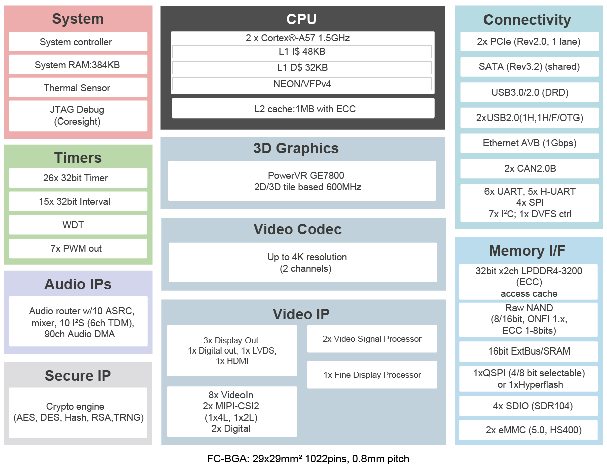
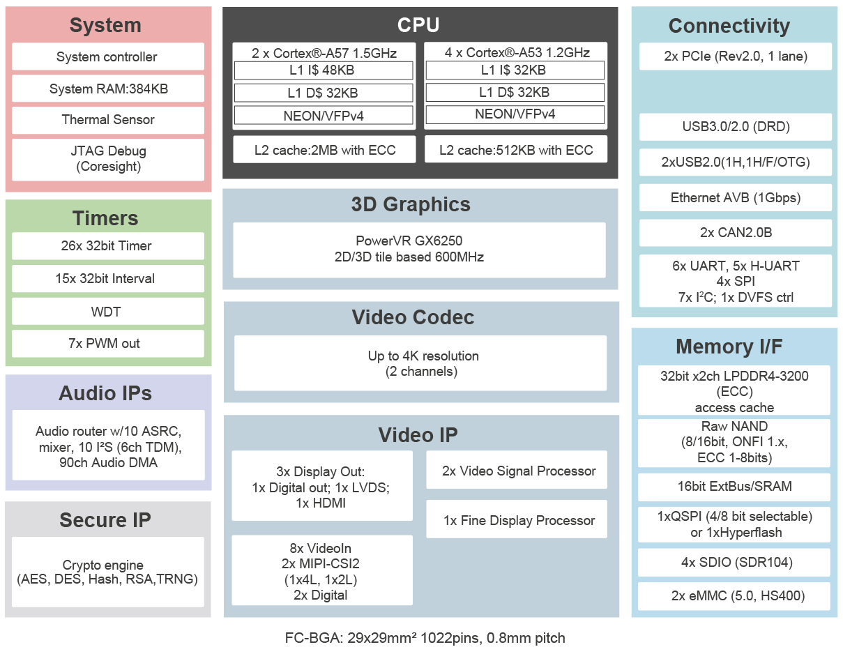
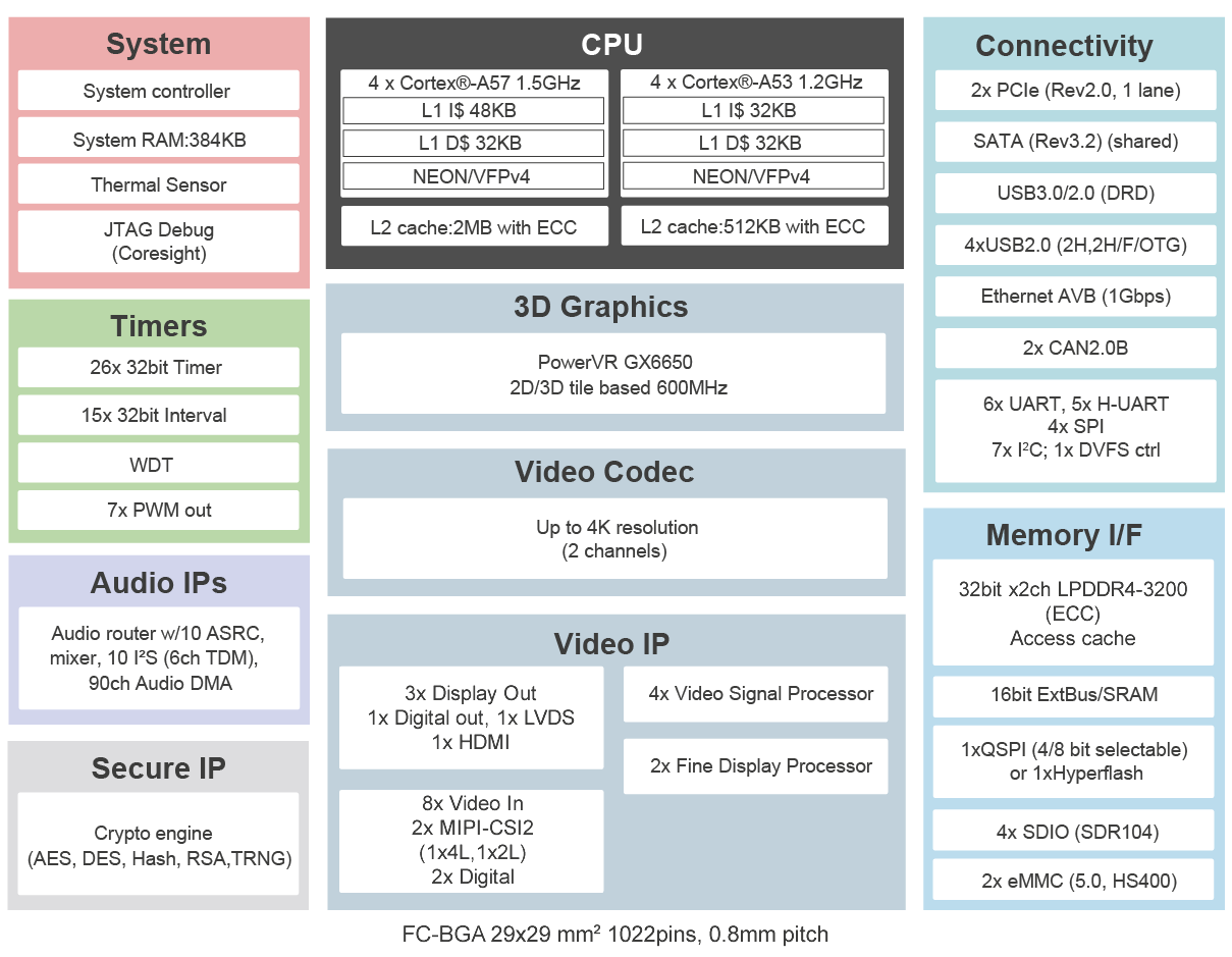