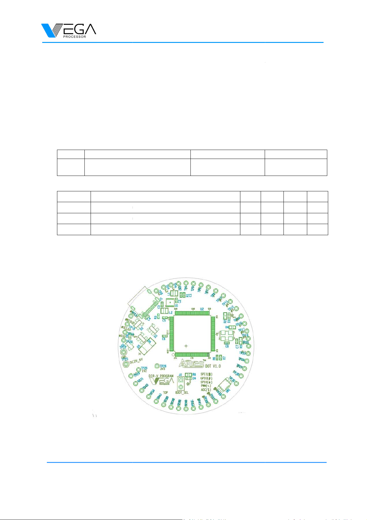
Vega ARIES DOT V1.0 User manual

ARIES DOT V1.0
© August, 2023 Centre for Development of Advanced Computing (C-DAC) Page | /
Product Reference Manual
Description
The ARIES DOT v1.0 is a circular development platform based on indigenousl developed THEJAS32
SoC and a “Made in India” product to get started with basic microprocessor programming and embedded
s stems. This board is built upon a RISC-V ISA compliant VEGA Processor with eas -to-use hardware and
software. The VEGA SDK also provides full ecos stem with numerous examples and support documentation.
This board is designed and developed b Centre for Development of Advanced Computing (C-DAC) as part of
the Digital India RISC-V (DIR-V) Program, b the Ministr of Electronics and Information Technolog ,
Government of India.
Target areas/Applications
Gesture controlled devices,Health monitoring devices,Low power IoT, Sensor fusion, Smart Meter,
S stem supervisors, Remote sensors, Wearable devices, To and electronic education equipment, Legac
8/16-bit applications, Industrial networking and man more…

ARIES DOT V1.0
© August, 2023 Centre for Development of Advanced Computing (C-DAC) Page | 2/
Features
Controller
THEJAS32 SoC with VEGA ET1031 Microprocessor
Memory
2MB Flash
256KB SRAM
Peripherals
•
PWM Pins : 8 nos
•
Analog Input Pins
: 4 nos
•
SPI : 2 nos
•
UART : 2 nos
•
I2C : 1 nos
•
GPIOs : 15 nos (14xGPIO, 1x LED)
Clock Speed
Clock Speed : 100MHz
Power
•
Input Voltage : 5 V DC
•
DC Current per I/O Pin
: 12 mA
•
IO Voltage : 3.3 V

ARIES DOT V1.0
© August, 2023 Centre for Development of Advanced Computing (C-DAC) Page | 3/
CONTENTS
1. The Board 4
2. Ratings 4
2.1 Recommended Operating Conditions 4
2.2 Power Consumption 4
3. Functional Overview 4
3.1 Board Topology 4
3.2 Processor 5
3.3 THEJAS32 pinout 5
3.4 Power Tree 8
4. Board Operation 8
4.1 Getting Started 8
5. Connector Pinouts 9
5.1 Board Outline & Mounting Holes 11
6. Company Information 11
7. Reference Documentation 12

© August, 2023
Centre for Development of Advanced Computing (C
1. The Board
ARIES DOT v1
.0 is
frequenc of 100MHz. THEJAS32 SoC includes VEGA ET1031 Microprocessor, 256KB internal SRAM, Three
UARTs, Four SPIs, Three TIMERs, Eight PWMs, Three I2C interfaces, 32 GPIOs etc. This board c
ever thing needed to support standalone operation. To get started simpl connect the board to a computer
with a Micro-C USB Cable or
a batter
2. Ratings
2.1 Recommended Operating Conditions
Symbol
Description
Conservative thermal limits for the
whole board:
2.2 Power Consumption
Symbol Description
VINMax
Maximum input voltage from VIN pad
VUSBMax
Maximum input voltage from USB connector
PMax
DC Current per I/O Pin
3. Functional Overview
3.1 Board Topology
Top view
ARIES
Centre for Development of Advanced Computing (C
-DAC)
.0 is
a development platform based on THEAJS32 ASIC which operates at a
frequenc of 100MHz. THEJAS32 SoC includes VEGA ET1031 Microprocessor, 256KB internal SRAM, Three
UARTs, Four SPIs, Three TIMERs, Eight PWMs, Three I2C interfaces, 32 GPIOs etc. This board c
ever thing needed to support standalone operation. To get started simpl connect the board to a computer
a batter
.
2.1 Recommended Operating Conditions
Min
Conservative thermal limits for the
-0 °C (100°F)
Min
Typ
Maximum input voltage from VIN pad
-
Maximum input voltage from USB connector
-
5.5
DC Current per I/O Pin
-
-
ARIES
DOT V1.0
Page | 4/
a development platform based on THEAJS32 ASIC which operates at a
frequenc of 100MHz. THEJAS32 SoC includes VEGA ET1031 Microprocessor, 256KB internal SRAM, Three
UARTs, Four SPIs, Three TIMERs, Eight PWMs, Three I2C interfaces, 32 GPIOs etc. This board c
ontains
ever thing needed to support standalone operation. To get started simpl connect the board to a computer
Max
85 °C ( 185°F)
Typ
Max Unit
-
5 V
5.5
V
-
12 mA

ARIES DOT V1.0
© August, 2023 Centre for Development of Advanced Computing (C-DAC) Page | 5/
Ref. Description Ref. Description
J1 USB C Connector U2 THEJAS32 SoC
J2 Boot Select Header U1 Regulator
SW1 Reset Button U4 100 MHz Oscillator
D1 LED D6 Processor HeartBeat LED
3.2 Processor
The main controller is THEAJS32 SoC which operates at a frequenc of 100MHz. It includes VEGA ET1031
Microprocessor, 256KB internal SRAM, Three UARTs, Four SPIs, Three TIMERs, Eight PWMs, Three I2C
interface, 32 GPIOs. Most of its pins are connected to the external headers, however some are reserved for
internal communication.
3.3 THEJAS32 pinout
Pin # Pin Name Pin Description
1
GPIO1(3)
General purpose
IO.
2
GPIO1(2)
General purpose IO.
3
PVSSIOC23
Ground reference for IO pins.
4
PVDDIO23
Positive suppl for IO pins. Connect to 3.3V suppl .
5
GPIO1(1)
General purpose IO.
6
GPIO1(0)
General purpose IO.
7
SPI3MOSI
SPI 3 Master Out Slave In.
8
PVDDC18
Positive suppl for logic. Connect to 1.2V suppl .
9
PVSSC18
Ground reference for logic.
10
SPI3MISO
SPI 3 Master In Slave Out.
11
SPI3CLK
SPI 3 Clock.
12
SPI3CSN
SPI 3 Chip Select.
13
PVSSIOC21
Ground reference for IO pins.
14
PVDDIO21
Positive suppl for IO
pins. Connect to 3.3V suppl .
15
BOOT
Boot select.
16
PROCBT
Heart beat signal.
17
TEDTUPD
Connect to GND.
18
PVDDC17
Positive suppl for logic. Connect to 1.2V suppl .
19
PVSSC17
Ground reference for logic.
20
TSTCLK
Connect to GND through a 1K resistor.
21
TJTAGTDO
JTAG TDO. Left unconnected.
22
TJTAGTMS
JTAG TMS. Connect to GND through a 1K resistor.
23
TJTAGTDI
JTAG TDI. Connect to GND through a 1K resistor.
24
PVSSIOC19
Ground reference for IO pins.
25 PVDDIO19 Positive suppl for IO pins. Connect to 3.3V suppl .
26
PVDDC16
Positive suppl for logic. Connect to 1.2V suppl .
27
PVSSC16
Ground reference for logic.
28
TJTAGTCK
JTAG TCK. Connect to GND through a 1K resistor
29
TJTAGTRST
JTAG TRST. Connect to GND through a 1K resistor
30
TSTMODE
Test mode select.
Connect to GND through a 1K resistor.
31
IIC2SDA
I2C 2 Serial Data.
32
IIC2SCL
I2C 2 Serial Clock.

ARIES DOT V1.0
© August, 2023 Centre for Development of Advanced Computing (C-DAC) Page | 6/
33
IIC0SCL
I2C 0 Serial Clock.
34
IIC0SDA
I2C 0 Serial Data.
35
PVSSC14
Ground reference for logic.
36
PVDDC14
Positive suppl for logic. Connect to 1.2V suppl .
37
PVDDIO17
Positive suppl for IO pins. Connect to 3.3V suppl .
38
PVSSIOC17
Ground reference for IO pins.
39
SPI1CSN
SPI 1 Chip Select.
40
SPI1CLK
SPI 1 Clock.
41
SPI1MISO
SPI 1 Master In Slave Out.
42
SPI1MOSI
SPI 1 Master Out Slave In.
43
RSTIN
Reset.
44
CLKSYS
S stem Clock.
45
URT1SOUT
UART 1 Serial Out / Transmit.
46
PVDDIO15
Positive suppl for IO pins. Connect to 3.3V suppl .
47
PVSSIOC15
Ground reference for IO pins.
48
PVSSC12
Ground reference for logic.
49
PVDDC12
Positive suppl for logic. Connect to 1.2V
suppl .
50
URT1SIN
UART 1 Serial In / Receive.
51
GPIO0(15)
General purpose IO.
52
GPIO0(14)
General purpose IO.
53
GPIO0(13)
General purpose IO.
54
GPIO0(12)
General purpose IO.
55
GPIO0(11)
General purpose IO.
56
PVSSC11
Ground reference for logic.
57
PVDDC11
Positive suppl for logic. Connect to 1.2V suppl .
58
GPIO0(10)
General purpose IO.
59
PVDDIO13
Positive suppl for IO pins. Connect to 3.3V suppl .
60
PVSSIOC13
Ground reference for IO pins.
61
GPIO0(9)
General purpose IO.
62
GPIO0(8)
General purpose IO.
63
GPIO0(7)
General purpose IO.
64
GPIO0(6)
General purpose IO.
65
GPIO0(5)
General purpose IO.
66
GPIO0(4)
General purpose IO.
67
PVSSC9
Ground reference for logic.
68
PVDDC9
Positive suppl for logic. Connect to 1.2V suppl .
69
PVDDIO11
Positive suppl for IO
pins. Connect to 3.3V suppl .
70
PVSSIOC11
Ground reference for IO pins.
71
GPIO0(3)
General purpose IO.
72
GPIO0(2)
General purpose IO.
73
GPIO0(1)
General purpose IO.
74
GPIO0(0)
General purpose IO.
75
PWM(7)
Pulse Width Modulation.
76
PWM(6)
Pulse Width
Modulation.
77
PWM(5)
Pulse Width Modulation.
78
PVSSC7
Ground reference for logic.
79
PVDDC7
Positive suppl for logic. Connect to 1.2V suppl .
80
PWM(4)
Pulse Width Modulation.

ARIES DOT V1.0
© August, 2023 Centre for Development of Advanced Computing (C-DAC) Page | 7/
81
PWM(3)
Pulse Width Modulation.
82
PWM(2)
Pulse Width Modulation.
83
PVDDIO8
IO
Power Suppl VDD pin.
84
PVSSIOC8
Ground reference for IO pins.
85
PWM(1)
Pulse Width Modulation.
86
PWM(0)
Pulse Width Modulation.
87
SPI0MOSI
SPI 0 Master Out Slave In.
88
PVSSC6
Ground reference for logic.
89
PVDDC6
Positive suppl for logic. Connect to 1.2V
suppl .
90
SPI0MISO
SPI 0 Master In Slave Out.
91
SPI0CLK
SPI 0 Clock.
92
SPI0CSN
SPI 0 Chip Select.
93
PVDDIO6
Positive suppl for IO pins. Connect to 3.3V suppl .
94
PVSSIOC6
Ground reference for IO pins.
95
IIC1SDA
I2C 1 Serial Data.
96
IIC1SCL
I2C 1 Serial
Clock.
97
SPI2MOSI
SPI 2 Master Out Slave In.
98
SPI2MISO
SPI 2 Master In Slave Out.
99
PVDDC4
Positive suppl for logic. Connect to 1.2V suppl .
100
PVSSC4
Ground reference for logic.
101
SPI2CLK
SPI 2 Clock.
102
SPI2CSN
SPI 2 Chip Select.
103
PVSSIOC4
Ground
reference for IO pins.
104
PVDDIO4
Positive suppl for IO pins. Connect to 3.3V suppl .
105
URT2SIN
UART 2 Serial In / Receive.
106
URT2SOUT
UART 2 Serial Out / Transmit.
107
URT0SIN
UART 0 Serial In / Receive.
108
URT0SOUT
UART 0 Serial Out / Transmit.
109
GPIO1(15)
General purpose IO.
110
GPIO1(14)
General purpose IO.
111
GPIO1(13)
General purpose IO.
112
PVDDC2
Positive suppl for logic. Connect to 1.2V suppl .
113
PVSSC2
Ground reference for logic.
114
PVSSIOC2
Ground reference for IO pins.
115
PVDDIO2
Positive suppl for IO
pins. Connect to 3.3V suppl .
116
GPIO1(12)
General purpose IO.
117
GPIO1(11)
General purpose IO.
118
GPIO1(10)
General purpose IO.
119
GPIO1(9)
General purpose IO.
120
GPIO1(8)
General purpose IO.
121
GPIO1(7)
General purpose IO.
122
GPIO1(6)
General purpose IO.
123
PVSSIOC0
Ground reference for IO pins.
124
PVDDIO0
Positive suppl for IO pins. Connect to 3.3V suppl .
125
PVDDC0
Positive suppl for logic. Connect to 1.2V suppl .
126
PVSSC0
Ground reference for logic.
127
GPIO1(5)
General purpose IO.
128
GPIO1(4)
General purpose
IO.

ARIES DOT V1.0
© August, 2023 Centre for Development of Advanced Computing (C-DAC) Page | 8/
3.4 Power Tree
4. Board Operation
4.1 Getting Started
To use Vega Arduino IDE for programming follow the steps given in the link below
•For Linux; https://bit.l /vega-linux
•For Windows; https://bit.l /vega-windows
To use Eclipse IDE for programming follow the steps given in the link below
•https://cdac-vega.gitlab.io/sdkuserguide.html
VIN_EXT/
VCC_USB
SWITCHING
REGULATOR
VCC_3.3V
VCC_1.2V
T
H
E
J
A
S
32
SoC
CP2 02N USB
TO UART
IC(silicon labs)
ADC
SPI Flash
LED

ARIES DOT V1.0
© August, 2023 Centre for Development of Advanced Computing (C-DAC) Page | 9/
5. Connector pinout
SL
NO. SPECI ICATIONS THEJAS 32 ARIES BOARD REMARKS
1
SPI (3)
SPI0_SS
TP_20
2
SPI0_SCLK
TP_18
3
SPI0_MISO
TP_16
4
SPI0_MOSI
TP_13
5
SPI1_SS
TP_
41
6
SPI1_SCLK
TP_39
7
SPI1_MISO
TP_37
8
SPI1_MOSI
TP_35
9
SPI3_SS
U5_1
Connected to SPI BOOT FLASH IC
1
0
SPI3_SCLK
U5_6
1
1
SPI3_MISO
U5_2
1
2
SPI3_MOSI
U5_5
1
3
I2C (2)
I2C0_
SCL
TP_41
1
4
I2C0_
SDA
TP_34
15
I2C2_SCL
U6_10
Connected to ADC IC
16
I2C2_SDA
U6_9

ARIES DOT V1.0
© August, 2023 Centre for Development of Advanced Computing (C-DAC) Page | 0/
17
UART (2)
UART0_RXD
U4
_
17
Connected to UART TO USB
INTERFACE IC
18
UART0_TXD
U4
_
18
19
UART1_RX
TP_3
0
20
UART1_TX
TP_32
21
PWM (8)
PWM[0]
TP_
29
22
PWM[1]
TP_
31
23
PWM[2]
TP_
8
24
PWM[3]
TP_
6
25
PWM[4]
TP_4
26
PWM[5]
TP_
2
27
PWM[6]
TP_
1
28
PWM[7]
TP_
3
29
GPIO (15)
GPIO0
TP_
5
30
GPIO1
TP_
7
31
GPIO2
TP_
9
32
GPIO3
TP_
10
33
GPIO4
TP_
11
34
GPIO5
TP_
12
35
GPIO6
TP_
14
36
GPIO7
TP_
15
37
GPIO8
TP_
17
38
GPIO9
TP_
19
39
GPIO10
TP_
21
40
GPIO11
TP_
23
41
GPIO12
TP_
24
42
GPIO13
TP_
27
43
GPIO14
D
1
_1
Connected to
LED
44
CLOCK
CLK_100M
U
3
_3
Connected to OSCILLATOR
45
RESET
SW1
Connected to RESET
46
HEART BEAT LED
PROC_HEART_BEAT
LD
6
_1
Connected to LED
47 BOOT SELECT BOOT_SEL J2_1 Connected to HEADER J2
4
8
ADC_CH0
_
T
P
_
4
2
4
9
ADC_C
H1
_
T
P
_
4
0
5
0
ADC_CH
2
_
T
P
_
3
8
5
1
ADC_CH
3
_
T
P
_
3
6

© August, 2023
Centre for Development of Advanced Computing (C
5.1
Board Outline & Mounting Holes
6. Company Information
Company name C-
DAC
Compan Address
Hardware Design Group
Centre for Development of Advanced Computing (
Thiruvananthapuram, Kerala
Fax: 0471
www.vegaprocessors.in
www.cdac.in
7.
Reference Documentation
Reference
ARIES DoT v1.0 details
https://vegaprocessors.in/devboards/ariesdot.html
ARIES
Centre for Development of Advanced Computing (C
-DAC)
Board Outline & Mounting Holes
(
Dimensions in mm[
DAC
Hardware Design Group
Centre for Development of Advanced Computing (
C
Thiruvananthapuram, Kerala
– 695033
Fax: 0471
-2723456 Email: [email protected]
www.vegaprocessors.in
www.cdac.in
Reference Documentation
Link
https://vegaprocessors.in/devboards/ariesdot.html
ARIES
DOT V1.0
Page | /
Dimensions in mm[
mil] )
C
-DAC)
https://vegaprocessors.in/devboards/ariesdot.html
Table of contents
Other Vega Lighting Equipment manuals
Popular Lighting Equipment manuals by other brands

FRC
FRC LGTR1A-Rev120606 instruction manual

iGuzzini
iGuzzini LIGHT UP - WALK instruction sheet

Kogan
Kogan SMARTERHOME KBE27RGBC1A user guide

Clevertronics
Clevertronics L10 LWFLED 2IPREM Series Installation & Maintenance Instruction Manual

HERA
HERA DS-2 User manual & installation guide

Lighttoys
Lighttoys Visual Poi Mini user manual