Yaesu VX-2R Manual

1
©2003 VERTEX STANDARD CO., LTD. EH015M90A
Technical Supplement
Specifications .................................................................................................................................................................. 2
Exploded View & Miscellaneous Parts ...................................................................................................................... 4
Connection Diagram...................................................................................................................................................... 5
Block Diagram ................................................................................................................................................................ 6
Circuit Description......................................................................................................................................................... 7
Alignment ...................................................................................................................................................................... 11
Board Units (Schematics, Layouts & Parts)
MAIN Unit................................................................................................................................................................ 17
FILTER Unit.............................................................................................................................................................. 33
SW Unit ..................................................................................................................................................................... 37
VCO Unit .................................................................................................................................................................. 39
Introduction
This manual provides the technical information necessary for servicing the VX-2R
VHF/UHF Ultra-Compact Dual-Band Transceiver with Wide Band Coverage.
Servicing this equipment requires expertise in handing surface-mount chip com-
ponents. Attempts by non-qualified persons to service this equipment may result
in permanent damage not covered by the warranty, and may be illegal in some
countries.
Two PCB layout diagrams are provided for each double-sided board in this trans-
ceiver. Each side of the board is referred to by the type of the majority of compo-
nents installed on that side (“Side A” or “Side B”). In most cases one side has only
chip components (surface-mount devices), and the other has either a mixture of
both chip and leaded components (trimmers, coils, electrolytic capacitors, ICs,
etc.), or leaded components only.
As described in the pages to follow, the advanced microprocessor design of the
VX-2R allows a complete alignment of this transceiver to be performed without
opening the case of the radio; all adjustments can be performed from the front
panel, using the “Alignment Mode” menu.
While we believe the information in this manual to be correct, VERTEX STAN-
DARD assumes no liability for damage that may occur as a result of typographical
or other errors that may be present. Your cooperation in pointing out any incon-
sistencies in the technical information would be appreciated.
Contents
VERTEX STANDARD CO., LTD.
4-8-8 Nakameguro, Meguro-Ku, Tokyo 153-8644, Japan
VERTEX STANDARD
US Headquarters
10900 Walker Street, Cypress, CA 90630, U.S.A.
International Division
8350 N.W. 52nd Terrace, Suite 201, Miami, FL 33166, U.S.A.
YAESU EUROPE B.V.
P.O. Box 75525, 1118 ZN Schiphol, The Netherlands
YAESU UK LTD.
Unit 12, Sun Valley Business Park, Winnall Close
Winchester, Hampshire, SO23 0LB, U.K.
VERTEX STANDARD HK LTD.
Unit 5, 20/F., Seaview Centre, 139-141 Hoi Bun Road,
Kwun Tong, Kowloon, Hong Kong
Downloaded by
RadioAmateur.EU

2
Specifications
General
Frequency Ranges:RX 0.5-1.8 MHz (BC Band)
(USA Version) 1.8-30 MHz (SW Band)
30-76 (59) MHz (50 MHz HAM)
76 (59)-108 MHz (FM)
108-137 MHz (Air Band)
137-174 MHz (144 MHz HAM)
174-222 MHz (VHF TV)
222-420 MHz (ACT1)
420-470 MHz (430 MHz HAM)
470-800 (729) MHz (UHF TV)
(758-774) MHz (UHF TV)
800-999 MHz (ACT2; USA Cellular Blocked)
TX 144-146 (148) MHz
430-440 (450) MHz
Channel Steps:5/9/10/12.5/15/20/25/50/100 kHz
Frequency Stability:±5 ppm (14 °F to +140 °C [–10 °C to +60 °C])
Repeater Shift:±600 kHz (144 MHz)
±1.6/5.0/7.6 MHz (430 MHz)
Emission Type:F2 , F3
Antenna Impedance:50 W
Supply Voltage:Nominal:3.7 V DC,
Negative Ground
Operating: 3.2 - 7.0 V,
Negative Ground (EXT DC Jack)
5.5 - 7.0 V,
Negative Ground (EXT DC Jack with Charging)
Current Consumption:150 mA (Receive)
58 mA (Standby, Saver Off)
20 mA (Standby, Saver On)
200 µA (Auto Power Off)
1.3 A (1.5 W Tx , 144 MHz) 3.7 V DC
1.8 A (3 W Tx , 144 MHz) 6.0 V DC
1.2 A (1 W Tx , 430 MHz) 3.7 V DC
1.5 A (2 W Tx , 430 MHz) 6.0 V DC
Operating Temperature:–4 °F to +140 °F (–20 °C to +60 °C)
Case Size (W x H x D): 1.9 x 3.2 x 0.9 inch (47 x 81 x 23 mm) (W/O knob & antenna)
Weight:4.6 oz (132 g) With FNB-82LI & antenna
Transmitter
RF Power Output:1.5 W (@ 3.7 V FNB-82LI 144 MHz)
3 W (@ 6.0 V EXT DC IN 144 MHz)
1 W (@ 3.7 V FNB-82LI 430 MHz)
2 W (@ 6.0 V EXT DC IN 430 MHz)
Modulation Type:Variable Reactance F2 , F3
Maximum Deviation:±5 kHz (F2, F3)
Spurious Emission:At least 60 dB below (HIGH)
At least 50 dB below (LOW)
Microphone Impedance:2 kW
Downloaded by
RadioAmateur.EU

3
Specifications
Receiver
Circuit Type:AM, NFM: Double-Conversion Superheterodyne
WFM: Triple-Conversion Superheterodyne
Intermediate Frequencies:1st 2nd 3rd
AM, NFM 47.25MHz 450 kHz –
WFM 45.8 MHz 10.7 MHz 1 MHz
Sensitivity:3 µV for 10 dB SN (0.5-30 MHz, AM)
0.35 µV TYP for 12 dB SINAD (30-54 MHz, NFM)
1 µV TYP for 12 dB SINAD (54-76 MHz, NFM)
1.5 µV TYP for 12 dB SINAD (76-108 MHz, WFM)
1.5 µV TYP for 10 dB SN (108-137 MHz, AM)
0.2 µV for 12 dB SINAD (137-140 MHz, NFM)
0.16 µV for 12 dB SINAD (140-150 MHz, NFM)
0.2 µV for 12 dB SINAD (150-174 MHz, NFM)
1 µV TYP for 12 dB SINAD (174-222 MHz, WFM)
0.5 µV for 12 dB SINAD (300-350 MHz, NFM)
0.2 µV for 12 dB SINAD (350-400 MHz, NFM)
0.18 µV for 12 dB SINAD (400-470 MHz, NFM)
1.5 µV for 12 dB SINAD (470-540 MHz, WFM)
3 µV TYP for 12 dB SINAD (540-800 MHz, WFM)
1.5 µV TYP for 12 dB SINAD (800 -999 MHz, NFM)
USA Version Cellular Blocked
Selectivity:NFM, AM: 12 kHz/35 kHz (–6 dB/–60 dB)
WFM: 200 kHz/300 kHz (–6 dB/–20 dB)
AF Output:50 mW @ 8 W for 10 % THD (@ 3.7 V)
100 mW @ 8 W for 10 % THD (@ 6.0 V)
Specifications are subject to change without notice, and are guaranteed within the 144 and 430 MHz amateur bands only.
Frequency ranges will vary according to transceiver version; check with your dealer.
Downloaded by
RadioAmateur.EU

4
Exploded View & Miscellaneous Parts
RA0111400
RING NUT
‰
REF
•
‚
ƒ
„
…
†
‡
ˆ
‰
VXSTD P/N
U07125302
U07180306
U07240302
U44110002
U9900044
U9900068
U9900153
U9900154
U9900156
DESCRIPTION
PAN HEAD SCREW M1.7X2.5NI#3
PAN HEAD SCREW M1.7X8AU#3
PAN HEAD SCREW M2X4NI#3
TAPTITE SCREW M2X15NI
TAPTITE SCREW 1.7X5NI#3 GUIDE
TAPTITE SCREW M2X4NI#3
SPECIAL SCREW M1.7X4SUS
SPECIAL SCREW M3X4SUS
PAN HEAD SCREW M2X11NI#3
QTY
1
1
1
2
2
3
1
1
1
RA0023500
RING NUT (SMA)
RA0503100
RUBBER CAP (SP)
RA0504400
ENCODER KNOB
RA0504000
FRAME (LCD)
RA0503500
LIGHT GUIDE (LCD)
G6090152
LCD
RA050410A
INTER CONNECTOR
RA0514400
HOLDER ASSY
RA0503200
RUBBER CAP (DC)
RA0503800
COVER
CP7639001
CHASSIS ASSY
RA0512100
BATTERY COVER ASSY
FILTER UNIT
MAIN UNIT
SW UNIT
RA0503000
RUBBER KNOB (KEY)
RA0503600
LATCH NAIL
RA0503300
RUBBER KNOB (PTT)
M3290039
MICROPHONE ELEMENT
RA0511800
SPONGE RUBBER
RA0504700
MASK SHEET
•
‚
ƒ
„
„
…
…
†
†
†
‡
ˆ
RA0518000
CASE ASSY
INCLUDE
RUBBER KNOB (PTT)
LATCH NAIL
( )
RA0034400
LCD SHEET
RA0504300
VOLUME KNOB

5
Connection Diagram
Downloaded by
RadioAmateur.EU

6
Block Diagram
Downloaded by
RadioAmateur.EU

7
Circuit Description
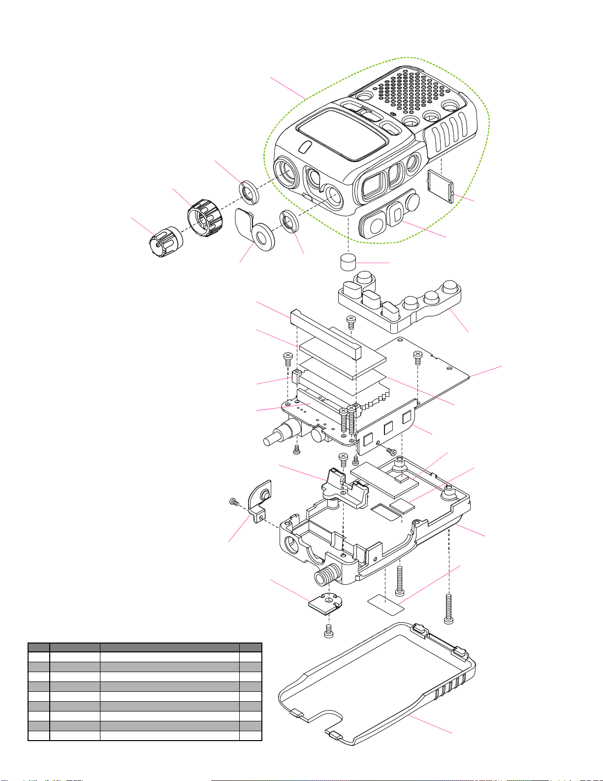
The VX-2R consists of a MAIN-UNIT, a FILTER-UNIT, a
SW-UNIT, and a VCO-UNIT. The MAIN-UNIT contains
the receiver front end, IF circuit, PLL circuit, the CPU,
audio ICs, and the power circuitry for the LCD. The FIL-
TER-UNIT contains the CTCSS/DCS Encoder/Decoder cir-
cuit. The SW-UNIT contains the TX power amplifier cir-
cuit and power switching circuits. The VCO-UNIT con-
tains the transmit/receive local signal oscillator and trans-
mit modulator circuit.
Receiver Signal Flow
The VX-2R includes four receiver front ends, each opti-
mized for a particular frequency range and mode combi-
nation.
(1)Triplexer
Signals between 0.5 and 540 MHz received at the antenna
terminal pass through a first low-pass filter composed of
L1053, L1056, C1300, and C1302.
Received 430-MHz signals, after passing through a low-
pass filter, are fed to the UHF T/R switch circuit composed
of diode switch D1057 (RLS135) and D1059 (1SV307).
Received 145-MHz signals, after passing through a low-
pass filter, are fed to the VHF T/R switch circuit composed
of diode switch D1058 (RLS135) and D1060 (1SV307).
(2)145-MHz Band and 76-300MHz Reception
Received signals between 140 and 150 MHz pass through
the Triplexer circuit, a low-pass filter/high-pass filter cir-
cuit, VHF T/R switch circuit, and protector diode D1002
(1SS362) before additional filtering by a band-pass filter
prior to application to RF amplifierQ1005 (2SC5555). The
amplified RF signal is passed through aband-pass filter
to first mixer Q1014 (2SC5555). Meanwhile, the first lo-
cal signal for the VHF band from the VCO-UNIT is am-
plified by Q1025 (2SC5374) and applied through diode
T/R switch D1041 (DAN222M) to mixer Q1014 (2SC5555)
as the first local signal.
The 47.25-MHz intermediate frequency product of the
mixer is delivered to the IF circuit.
The TUNE voltage from the CPU is amplified by DC am-
plifier Q1016 (NJU7007) and applied to varactors D1020
(1SV325), D1021 (1SV325), D1022 (HVC369), D1023
(1SV325), D1024 (1SV325), D1025 (HVC369), D1034
(1SV325),and D1035 (1SV325) in the variable frequency
band-pass filters. By changing the electrostatic capacitance
of the varactors, optimum filter characteristics are pro-
vided for each specific operating frequency.
(3)435-MHz Band and 300-540MHz Reception
Received signals between 430 and 450 MHz pass through
the Triplexer circuit, a low-pass filter/high-pass filter cir-
cuit, UHF T/R switch circuit,and protector diode D1001
(1SS362) before additional filtering by a band-pass filter
prior to application to RF amplifierQ1004 (2SC5555). The
amplified RF signal is passed through aband-pass filter,
RF amplifier Q1008 (2SC5555),and another band-pass
filter to first mixer Q1013 (2SC5555). Meanwhile, the first
local signal for the UHF band from the VCO-UNIT is
amplified by Q1024 (2SC5374) and applied through di-
ode T/R switch D1040 (HN2D01FU) to mixer Q1013
(2SC5555) as the first local signal.
The 47.25-MHz intermediate frequency product of the
mixer is delivered to the IF circuit.
The TUNE voltage from the CPU is amplified by DC am-
plifier Q1016 (NJU7007) and applied to varactors D1018,
D1019, D1032,and D1033 (all HVC358) in the variable
frequency band-pass filters. By changing the electrostatic
capacitance of the varactors, optimum filter characteris-
tics are provided for each specific operating frequency.
(4)0.5-76 MHz Reception
Received signals between 0.5 and 76 MHz pass through
the Triplexer circuit, alow-pass filter circuit, T/R switch
circuit,and protector diode D1003 (1SV307) before addi-
tional filtering by a band-pass filter prior to application to
RF amplifier Q1009 (2SC5555). The amplified RF signal
is passed through the band-pass filter to first mixerQ1015
(2SC5555). Meanwhile, the first local signal for the BC/
SW band from the VCO-UNIT is amplified by Q1026
(2SC5374)and fed to mixer Q1015 (2SC5555) as the first
local signal.
The 47.25-MHz intermediate frequency product of the
mixer is delivered to the IF circuit.
The TUNE voltage from the CPU is amplified by DC am-
plifier Q1016 (NJU7007)and applied to varactors D1026
(HVR100) in the variable frequency band-pass filters. By
changing the electrostatic capacitance of the varactors, op-
timum filter characteristics are provided for each specific
operating frequency.
(5)540 - 999 MHz Reception
Received signals between 540 and 999 MHz pass through
ahigh-pass filter circuit and T/R switch D1005 (1SV271)
prior to application to RF amplifierQ1002 (2SC5277). The
amplified RF signal is passed through aband-pass filter
to first mixer Q1012 (2SC5277). Meanwhile, the first lo-
cal signal for the UHF band from the VCO-UNIT is am-
plified by Q1024 (2SC5374) and applied through diode
T/R switchD1040 (HN2D01FU) to mixerQ1012 (2SC5277)
as the first local signal.
The 47.25-MHz intermediate frequency product of the
mixer is delivered to the IF circuit.
The TUNE voltage from the CPU on the CNTL-UNIT is
amplified by DC amplifier Q1016 (NJU7007) and applied

8
Circuit Description
to varactors D1016 and D1017 (both HVC355B) in the
variable frequency band-pass filters. By changing the elec-
trostatic capacitance of the varactors, optimum filter char-
acteristics are provided for each specific operating fre-
quency.
(6)47.25-MHz First Intermediate Frequency
The 47.25-MHz first intermediate frequency from first
mixers is delivered to the first IF circuit. On the MAIN-
UNIT, the first IF signals onthe AM and FM-narrow are
passed through NAR/WIDE switch D1037 (DAP222M),
47.25-MHz monolithic crystal filter (MCF) XF1001, and
narrow IF amplifier Q1017 (2SC4915) to pin 16 of Nar-
row IF IC Q1033 (TA31136FN) after amplitude limiting
by D1042 (DA221M).
Meanwhile, a portion of the output of 11.7-MHz crystal
X1001 is multiplied fourfold by Q1035 and Q1022 (both
2SC4915) to provide the 46.8-MHz second local signal,
applied to the Narrow IF IC Q1033 (TA31136FN). Within
this IC, the 46.8-MHz second local signal is mixed with
the 47.25-MHz first intermediate frequency signal to pro-
duce the 450-kHz second intermediate frequency.
This second IF signal is filtered by ceramic filter CF1002
and amplified by the limiting amplifier within the Nar-
row IF IC Q1033 (TA31136FN) before quadrature detec-
tion by ceramic discriminator CD1001.
Demodulated audio is fed from pin 9 of the Narrow IF IC
Q1033 (TA31136FN) through the “narrow mute”analog
switch Q1044 and squelch gate Q1053 (both 2SJ364) be-
fore de-emphasis at Q1039 (DTC144EM).
The resulting audio is amplified by AF amplifier Q1079
(NJM2135V), and fed through MIC/EAR jack J1007 to the
internal speaker,SP1001,or an external earphone.
(7)Squelch Control
Signal components in the neighborhood of 15 kHz con-
tained in the discriminator output pass through an active
band-pass filter composed of R1142, R1156, R1160, C1168,
C1177, and the operational amplifier between pins 7 and
8 within Narrow IF IC Q1033 (TA31136FN). They are then
rectified by D1049 and D1050 (both DA221M) to obtain a
DC voltage corresponding to the level of noise. This volt-
age is fed to pin 51 of CPU Q1076 (HD64F2266), which
compares the input voltage with a previously set thresh-
old. When the input voltage drops below the threshold,
normally due to the presence of a carrier, squelch gate
Q1071 (2SC4617) turns on and allowsany demodulated
audio to pass. At the same time, Q1001 (UMW1N) switch-
es on, causing the BUSY/TX lampD1004 (CL-165) to light.
Transmitter Signal Flow
(1)145-MHz-Band T/R Switching
Closing PTT switch S3001 on the SW-UNIT pulls the base
of Q1007 (DTA114EM) low, causing the collector to go
high. This signal is fed to pin 45 (PTT) of CPU Q1076
(HD64F2266), allowing the CPU to recognize that the PTT
switch has been pushed. When the CPU detects closure of
the PTT switch, pin 70 (TX/RX) goes high. This control
signal switches Q1054 (UMD6N) to produce the TX con-
trol signal that activates Q1050 (2SA1774). At the same
time, PLL division data is applied to PLL IC Q1034
(MB15A01PFV) from the CPU, to disable the receiver
power saver. Also,Q1049 (EMG2) is switched on to dis-
able the receiver circuits,causing the red side of BUSY/
TX lamp D1004 (CL-165) to light.
(2)Modulation
Voice signal input from either the built-in microphone
MC1001 on the MAIN-UNIT or external microphone in-
put from external mic jack J1007 is pre-emphasized by
C1036 and R1031, and processed by microphone amplifi-
er Q1083 (NJM3403AV), the IDC (instantaneous devia-
tion control) circuit Q1083 to prevent over-modulation,
and active low-pass filter Q1083.
During CTCSS operation, the voice signal is mixed with
the TONE ENC subaudible tone signal from pin 43 of the
CPU and delivered to the VCO. During DCS operation,
the voice signal is mixed with the DCS ENC subaudible
tone signal from pin 44 of the CPU and delivered to the
VCO. During DTMF operation, the DTMF tones from pin
44 of the CPU are fed directly to the IDC stage.
(3)145-MHz-Band Transmission
Modulating audio passes through deviation setting D/A
converter Q1010 (M62364FP), then delivered to the VHF
modulator of the VCO-UNIT mounted on the MAIN-
UNIT. This signal is applied to varactor D4005 (HSC277)
in the tank circuit of VHF VCO Q4004 (EC3H07B), which
oscillates at the desired VHF transmitting frequency. The
modulated VCO signal is buffered by amplifier Q4006
(EC3H07B) and Q1025 (2SC5374) and delivered through
VHF T/R diode switch D1041 (DAN222M) to the MAIN-
UNIT. The modulated low-level VHF transmit signal from
the VCO is passed through diode switch D1047
(DAN222M) to amplifier Q3004 (2SC5374) on the SW-
UNIT. The amplified VHF transmit signal from Q3004
(2SC5374) is amplified byQ3001 (2SC5226) and RF pow-
er amplifier Q3002 (2SK3079) on the SW-UNIT up to 0.1,
0.3, 1.5, or 3 Watts (depending on the power source). The
RF output passes through TX diode switch D1058
(RLS135) then fed via the T/R switch and low-pass filter
(to suppress harmonics and spurious products)to the an-
tenna terminal.

9
(4)435-MHz-Band Transmission
Modulating audio passes through deviation setting D/A
converter Q1010 (M62364FP) then delivered to the UHF
modulator of the VCO-UNIT mounted on the MAIN-
UNIT. This signal is applied to varactor D4002 (HSC277)
in the tank circuit of UHF VCO Q4002 (EC3H07B), which
oscillates at the desired UHF transmitting frequency. The
modulated VCO signal is buffered by amplifier Q4006
(EC3H07B) and Q1024 (2SC5374) and delivered through
UHF T/R diode switch D1040 (HN2D01FU) to the MAIN-
UNIT. The modulated low-level UHF transmit signal from
the VCO is passed through diode switch D1047
(DAN222M) to amplifier Q3004 (2SC5374) on the SW-
UNIT. The amplified UHF transmit signal from Q3004
(2SC5374) is amplified byQ3001 (2SC5226) and RF pow-
er amplifier Q3002 (2SK3079) on the SW-UNIT up to 0.1,
0.3, 1.0, or 2 Watts (depending on the power source). The
RF output passes through TX diode switch D1057
(RLS135) then fed via the T/R switch and low-pass filter
to the antenna terminal.
PLL Frequency Synthesizer
PLL IC Q1034 (MB15A01PFV) on the MAIN-UNIT con-
sists of a data shift register, reference frequency divider,
phase comparator, charge pump, intermittent operation
circuit, and band selector switch. Serial PLL data from the
CPU is converted into parallel data by the shift register in
the PLL IC Q1034 (MB15A01PFV) and is latched into the
comparative frequency divider and reference frequency
divider to set a frequency dividing ratio for each. An 11.7-
MHz reference signal produced by X1001 is fed to REF
pin 1 of the PLL IC Q1034 (MB15A01PFV). The internal
reference frequency divider divides the 11.7-MHz refer-
ence by 2,050 (or 1,640) to obtain a reference frequency of
5 kHz (or 6.25 kHz), which is applied to the phase com-
parator. Meanwhile, a sample of the output of VHF VCO
Q4004 or UHF VCO Q4002 (both EC3H07B) on the VCO-
UNIT, buffered by Q4007 (DTC144ZE), is fed to the PLL
IC, where the frequency is divided by the internal com-
parative frequency divider to produce a comparison fre-
quency which also is applied to the phase comparator.
The phase comparator compares the phase between the
reference frequency and comparison frequency to output
a pulse corresponding to the phase difference between
them. This pulse is fed to the charge pump, and the out-
put from the charge pump passes through a loop filter
composed of L1036, R1152, C1166, and either R1153,
C1167, R1172 and C1193,for VHF, or R1149, C1162, R1171,
and C1192 for UHF, which convertsthe pulse into a cor-
responding smoothed varactor control voltage (VCV). The
VCV is applied to varactor D4004 and D4013 (both
1SV325) in the VHF VCO tank circuit, or to varactor D4001
(HVC355B) in the UHF VCO tank circuit, to eliminate
phase difference between the reference frequency and
comparative frequency, thus locking the VCO oscillation
frequency to the reference crystal. The VCO frequency is
determined by the frequency-dividing ratio sent from the
CPU to the PLL IC. During receiver power save opera-
tion, the PLL circuit operates intermittently to reduce cur-
rent consumption, for which the intermittent operation
control circuit reduces the lock-up time.
Circuit Description

10
Circuit Description
Note

11
Alignment
Introduction
The VX-2R is carefully aligned at the factory for the spec-
ified performance across the amateur band. Realignment
should therefore not be necessary except in the event of a
component failure. Only an authorized Vertex Standard
representative should perform all component replacement
and service, or the warranty policy may be void.
The following procedures cover the adjustments that are
not normally required once the transceiver has left the fac-
tory. However, if damage occurs and some parts subse-
quently are replaced, realignment may be required. If a
sudden problem occurs during normal operation, it is like-
ly due to component failure; realignment should not be
done until after the faulty component has been replaced.
We recommend that servicing be performed only by au-
thorized Vertex Standard service technicians who are ex-
perienced with the circuitry and fully equipped for re-
pair and alignment. If a fault is suspected, contact the deal-
er from whom the transceiver was purchased for instruc-
tions regarding repair. Authorized Vertex Standard ser-
vice technicians realign all circuits and make complete
performance checks to ensure compliance with factory
specifications after replacing any faulty components.
Those who do undertake any of the following alignments
are cautioned to proceed at their own risk. Problems
caused by unauthorized attempts at realignment are not
covered by the warranty policy. Also, Vertex Standard
reserves the right to change circuits and alignment proce-
dures in the interest of improved performance, without
notifying owners.
Under no circumstances should any alignment be attempt-
ed unless the normal function and operation of the trans-
ceiver are clearly understood, the cause of the malfunc-
tion has been clearly pinpointed and any faulty compo-
nents replaced, and realignment determined to be abso-
lutely necessary.
Required Test Equipment
The following test equipment (and familiarity with its use)
is necessary for complete realignment. Correction of prob-
lems caused by misalignment resulting from use of im-
proper test equipment is not covered under the warranty
policy. While most steps do not require all of the equip-
ment listed, the interactions of some adjustments may re-
quire that more complex adjustments be performed after-
wards.
Do not attempt to perform only a single step unless it is
clearly isolated electrically from all other steps. Have all
test equipment ready before beginning and, follow all of
the steps in a section in the order presented.
rRF Signal Generator with calibrated output level at 500
MHz
rDeviation Meter (linear detector)
rIn-line Wattmeter with 5% accuracy at 500 MHz
r50-Ohm 10-W RF Dummy Load
r8-Ohm AF Dummy Load
rRegulated DC Power Supply adjustable from 3 to 15
VDC, 2A
rFrequency Counter: 0.2-ppm accuracy at 500 MHz
rAF Signal Generator
rAC Voltmeter
rDC Voltmeter: high impedance
rUHF Sampling Coupler
rSINAD Meter
Alignment Preparation & Precautions
A 50-Ohm RF load and in-line wattmeter must be con-
nected to the main antenna jack in all procedures that call
for transmission;alignment is not possible with an anten-
na. After completing one step, read the next step to see if
the same test equipment is required. If not, remove the
test equipment (except dummy load and wattmeter, if
connected) before proceeding.
Correct alignment requires that the ambient temperature
be the same as that of the transceiver and test equipment,
and that this temperature be held constant between 68 ~
86° F (20° ~ 30° C). When the transceiver is brought into
the shop from hot or cold air, it should be allowed some
time to come to room temperature before alignment.
Whenever possible, alignments should be made with os-
cillator shields and circuit boards firmly affixed in place.
Also, the test equipment must be thoroughly warmed up
before beginning.
Note:Signal levels in dB referred to in the alignment pro-
cedure are based on 0dBm = 0.5µV.
Test Setup
Set up the test equipment as shown below for transceiver
alignment, and apply 4.4 V DC power to the transceiver.
Refer to the drawings for Alignment Points.
8-ohm AF
Dummy Load
RF Signal
Generator
SINAD Meter
In-Line
Wattmeter
Deviation
Meter
50-ohm RF
Dummy Load
Frequency
Counter
AF Signal
Generator
Regulated
4.4 VDC P.S.
AF Signal Input
AF Signal Output

12
Alignment
Internal System Alignment Routine
This process uses a programmed routine in the transceiv-
er which simplifies many previously complex discrete
component settings and adjustments with digitally-con-
trolled settings via front panel keys and LCD indications.
Set the transceiver to the 430MHz band, then turn the
transceiver off. Now, press and hold in the [F/W], [MD],
and [ ] keys(at the same time) while powering the radio
on again. The display will show the first setting. Thereaf-
ter, the frequencies used during alignment will automat-
ically be set without further action by the technician.
In the alignment process, each adjustment is selected by
rotating the DIAL knob. Alignment is performed by:
¦Pressing the [V/M]key;
¦Injecting a signal of the required frequency and level;
then
¦Pressing the [V/M]key after a level setting or adjust-
ment is made. This second pressing of the [V/M]key
storesthe alignment data at the desired value.
To exit the alignment routine, press the [HM/RV]key. Af-
ter performing the system alignment in its entirety, indi-
vidual settings can be returned to and adjusted should
the need arise.
PLL Reference Frequency (PLL REF)
rPress the [V/M]key.
rTransmit, and adjust the counter frequency to within
±300 Hz by rotating the DIAL knob;now press the
[V/M]key.
rRotate the DIAL knob to select the next setting.
430 MHz Band Alignment
Squelch Hysteresis Adjust (HIS)
rPress the [V/M]key.
rRotate the DIAL knob for minimum squelch hysteresis,
then press the [V/M]key.
rRotate the DIAL knob to select the next setting.
Squelch Preset Threshold (tHL)
rPress the [V/M]key.
rInject a 435.1 MHz, –12 dBµ RF signal (1 kHz tone @
±3.5 kHz deviation) to the ANT jack, then press the
[F/W]key.
rPress the [F/W]key again, then press the [V/M]key.
rRotate the DIAL knob to select the next setting.
Squelch Preset Tight (tIg)
rPress the [V/M]key.
rAdjust the generator level for a –5 dBµ signal (leaving
the modulation level unchanged), then press the
[F/W]key.
rPress the [F/W]key again, then press the [V/M]key.
rRotate the DIAL knob to select the next setting.
Low-Scale S-1 Adjustment (S1)
rPress the [V/M]key.
rAdjust the generator level to –7 dBµ(leaving the modu-
lation level unchanged), then press the [F/W]key.
rPress the [F/W]key again, then press the [V/M]] key.
rRotate the DIAL knob to select the next setting.
S-Meter Full-Scale Adjustment (S9)
rPress the [V/M]key.
rAdjust the generator level to +20 dBµ (leaving the
modulation level unchanged), then press the[F/W]key.
rPress the [F/W]key again, then press the [V/M]key.
rRotate the DIAL knob to select the next setting.
Wide FM Low-Scale S-1 Adjustment (S1)
rPress the [V/M]key.
rAdjust the generator level to 0 dBµ (1 kHz tone @ ±20
kHz deviation), then press the [F/W]key.
rPress the [F/W]key again, then press the [V/M]key.
rRotate the DIAL knob to select the next setting.
Wide FM S-Meter Full-Scale Adjustment (S9)
rPress the [V/M]key.
rAdjust the generator level to +20 dBµ (leaving the
modulation level unchanged from the previous step),
then press the [F/W]key.
rPress the [F/W]key again, then press the [V/M]key.
rRotate the DIAL knob to select the next setting.
TX High Power (Low Band Edge @6.0 V) Adjustment (HHP)
rSet the DC power supply voltage to 6.0 V.
rPress the [V/M]key.
rTransmit, and adjust the output power level for 2.0 W
(±0.2 W) by rotating the DIAL knob, then press the
[V/M]key.
rRotate the DIAL knob to select the next setting.
TX High Power (Low Band Edge @4.4 V) Adjustment (LHP)
rSet the DC power supply voltage to 4.4 V.
rPress the [V/M]key.
rTransmit, and adjust the output power level for 1.0 W
(±0.1 W) by rotating the DIAL knob, then press the
[V/M]key.
rRotate the DIAL knob to select the next setting.

13
TX Low Power (Low Band Edge) Adjustment (LP)
rPress the [V/M]key.
rTransmit, and adjust the output power level for 0.1 W
(±0.05 W) by rotating the DIAL knob, then press the
[V/M]key.
rRotate the DIAL knob to select the next setting.
TX Deviation (Low Band Edge) Adjustment (dEV)
rPress the [V/M]key.
rInject a 1 kHz audio tone at a level of 50 mV (rms) to
the MIC jack, then press the [F/W]key.
rTransmit, and adjust the deviation for ±4.2 kHz (±0.2
kHz)by rotating the DIAL knob, then press the [V/M]
key.
rRotate the DIAL knob to select the next setting.
CTCSS Tone (67.0 Hz) Deviation (Low Band Edge)
Adjustment (670)
rPress the [V/M]key.
rTransmit, and adjust the deviation for ±0.6 kHz (±0.05
kHz)by rotating the DIAL knob, then press the [V/M]
key.
rRotate the DIAL knob to select the next setting.
CTCSS Tone (123.0 Hz) Deviation (Low Band Edge)
Adjustment (123)
rPress the [V/M]key.
rTransmit, and adjust the deviation for ±0.6 kHz (±0.05
kHz)by rotating the DIAL knob, then press the [V/M]
key.
rRotate the DIAL knob to select the next setting.
CTCSS Tone (254.1 Hz) Deviation (Low Band Edge)
Adjustment (254)
rPress the [V/M]key.
rTransmit, and adjust the deviation for ±0.6 kHz (±0.05
kHz)by rotating the DIAL knob, then press the [V/M]
key.
rRotate the DIAL knob to select the next setting.
DCS Tone Deviation (Low Band Edge) Adjustment (dCS)
rPress the [V/M]key.
rTransmit, and adjust the deviation for ±0.6 kHz (±0.05
kHz)by rotating the DIAL knob, then press the [V/M]
key.
rRotate the DIAL knob to select the Menu Item “HHP,”
then press the [F/W]key.
TX High Power (High Band Edge @6.0 V) Adjustment (HHP)
rSet the DC power supply voltage to 6.0 V.
rPress the [V/M]key.
rTransmit, and adjust the output power level for 2.0 W
(±0.2 W)by rotating the DIAL knob, then press the
[V/M]key.
rRotate the DIAL knob to select the next setting.
TX High Power (High Band Edge @4.4 V) Adjustment (LHP)
rSet the DC power supply voltage to 4.4 V.
rPress the [V/M]key.
rTransmit, and adjust the output power level for 1.0 W
(±0.1 W) by rotating the DIAL knob, then press the
[V/M]key.
rRotate the DIAL knob to select the next setting.
TX Low Power (High Band Edge) Adjustment (LP)
rPress the [V/M]key.
rTransmit, and adjust the output power level for 0.1 W
(±0.05 W)by rotating the DIAL knob, then press the
[V/M]key.
rRotate the DIAL knob to select the next setting.
TX Deviation (High Band Edge) Adjustment (dEV)
rPress the [V/M]key.
rInject a 1 kHz audio tone at a level of 50 mV (rms) to
the MIC jack, then press the [F/W]key.
rTransmit, and adjust the deviation for ±4.2 kHz (±0.2
kHz)by rotating the DIAL knob, then press the [V/M]
key.
rRotate the DIAL knob to select the next setting.
CTCSS Tone (67.0 Hz) Deviation (High Band Edge)
Adjustment (670)
rPress the [V/M]key.
rTransmit, and adjust the deviation for ±0.6 kHz (±0.05
kHz)by rotating the DIAL knob, then press the [V/M]
key.
rRotate the DIAL knob to select the next setting.
CTCSS Tone (123.0 Hz) Deviation (High Band Edge)
Adjustment (123)
rPress the [V/M]key.
rTransmit, and adjust the deviation for ±0.6 kHz (±0.05
kHz)by rotating the DIAL knob, then press the [V/M]
key.
rRotate the DIAL knob to select the next setting.
Alignment

14
CTCSS Tone (254.1 Hz) Deviation (High Band Edge)
Adjustment (254)
rPress the [V/M]key.
rTransmit, and adjust the deviation for ±0.6 kHz (±0.05
kHz)by rotating the DIAL knob, then press the [V/M]
key.
rRotate the DIAL knob to select the next setting.
DCS Tone Deviation (High Band Edge) Adjustment (dCS)
rPress the [V/M]key.
rTransmit, and adjust the deviation for ±0.6 kHz (±0.05
kHz)by rotating the DIAL knob, then press the [V/M]
key.
rRotate the DIAL knob to select the Menu Item “HIS,”
then press the [BAND]key.
50MHz Band Alignment (Receive Only)
Squelch Hysteresis Adjust (HIS)
rPress the [V/M]key.
rRotate the DIAL knob for minimum squelch hysteresis,
then press the [V/M]key.
rRotate the DIAL knob to select the next setting.
Squelch Preset Threshold (tHL)
rPress the [V/M]key.
rInject a 52.1 MHz, –10 dBµ RF signal (1 kHz tone @
±3.5 kHz deviation) to the ANT jack, then press the
[F/W]key.
rPress the [F/W]key again, then press the [V/M]key.
rRotate the DIAL knob to select the next setting.
Squelch Preset Tight (tIg)
rPress the [V/M]key.
rAdjust the generator level for a 0 dBµ signal (leaving
the modulation level unchanged), then press the
[F/W]key.
rPress the [F/W]key again, then press the [V/M]key.
rRotate the DIAL knob to select the next setting.
Low-Scale S-1 Adjustment (S1)
rPress the [V/M]key.
rAdjust the generator level to –2 dBµ (leaving the modu-
lation level unchanged), then press the [F/W]key.
rPress the [F/W]key again, then press the [V/M]key.
rRotate the DIAL knob to select the next setting.
S-Meter Full-Scale Adjustment (S9)
rPress the [V/M]key.
rAdjust the generator level to +20 dBµ (leaving the
modulation level unchanged), then press the[F/W]key.
rPress the [F/W]key again, then press the [V/M]key.
rRotate the DIAL knob to select the next setting.
Wide FM Low-Scale S-1 Adjustment (S1)
rPress the [V/M]key.
rAdjust the generator level to +8 dBµ (1 kHz tone @ ±20
kHz deviation), then press the [F/W]key.
rPress the [F/W]key again, then press the [V/M]key.
rRotate the DIAL knob to select the next setting.
Wide FM S-Meter Full-Scale Adjustment (S9)
rPress the [V/M]key.
rAdjust the generator level to +25dBµ (leaving the
modulation level unchanged from the previous step),
then press the [F/W]key.
rPress the [F/W]key again, then press the [V/M]key.
rPress the [BAND]key to select the next setting.
144MHz Band Alignment
Squelch Hysteresis Adjustment (HIS)
rPress the [V/M]key.
rRotate the DIAL knob for minimum squelch hysteresis,
then press the [V/M]key.
rRotate the DIAL knob to select the next setting.
Squelch Preset Threshold (tHL)
rPress the [V/M]key.
rInject a 145.1 MHz, –15 dBµ RF signal (1 kHz tone @
±3.5 kHz deviation) to the ANT jack, then press the
[F/W]key.
rPress the [F/W]key again, then press the [V/M]key.
rRotate the DIAL knob to select the next setting.
Squelch Preset Tight (tIg)
rPress the [V/M]key.
rAdjust the generator level for a –4 dBµ signal (leaving
the modulation level unchanged), then press the
[F/W]key.
rPress the [F/W]key again, then press the [V/M]key.
rRotate the DIAL knob to select the next setting.
Low-Scale S-1 Adjustment (S1)
rPress the [V/M]key.
rAdjust the generator level to –7 dBµ (leaving the modu-
lation level unchanged), then press the [F/W]key.
rPress the [F/W]key again, then press the [V/M]key.
rRotate the DIAL knob to select the next setting.
S-Meter Full-Scale Adjustment (S9)
rPress the [V/M]key.
rAdjust the generator level to +20 dBµ (leaving the
modulation level unchanged), then press the[F/W]key.
rPress the [F/W]key again, then press the [V/M]key.
rRotate the DIAL knob to select the next setting.
Alignment

15
Wide FM Low-Scale S-1 Adjustment (S1)
rPress the [V/M]key.
rAdjust the generator level to 0 dBµ (1 kHz tone @ ±20
kHz deviation), then press the [F/W]key.
rPress the [F/W]key again, then press the [V/M]key.
rRotate the DIAL knob to select the next setting.
Wide FM S-Meter Full-Scale Adjustment (S9)
rPress the [V/M]key.
rAdjust the generator level to +20dBµ (leaving the
modulation level unchanged from the previous step),
then press the [F/W]key.
rPress the [F/W]key again, then press the [V/M]key.
rRotate the DIAL knob to select the next setting.
TX High Power (Low Band Edge @6.0 V) Adjustment (HHP)
rSet the DC power supply voltage to 6.0 V.
rPress the [V/M]key.
rTransmit, and adjust the output power level for 3.0 W
(±0.2 W) by rotating the DIAL knob, then press the
[V/M]key.
rRotate the DIAL knob to select the next setting.
TX High Power (Low Band Edge @4.4 V) Adjustment (LHP)
rSet the DC power supply voltage to 4.4 V.
rPress the [V/M]key.
rTransmit, and adjust the output power level for 1.5 W
(±0.1 W) by rotating the DIAL knob, then press the
[V/M]key.
rRotate the DIAL knob to select the next setting.
TX Low Power (Low Band Edge) Adjustment (LP)
rPress the [V/M]key.
rTransmit, and adjust the output power level for 0.1 W
(±0.05 W) by rotating the DIAL knob, then press the
[V/M]key.
rRotate the DIAL knob to select the next setting.
TX Deviation (Low Band Edge) Adjustment (dEV)
rPress the [V/M]key.
rInject a 1 kHz audio tone at a level of 50 mV (rms) to
the MIC jack, then press the [F/W]key.
rTransmit, and adjust the deviation for ±4.2 kHz (±0.2
kHz) by rotating the DIAL knob, then press the [V/M]
key.
rRotate the DIAL knob to select the next setting.
CTCSS Tone (67.0 Hz) Deviation (Low Band Edge)
Adjustment (670)
rPress the [V/M]] key.
rTransmit, and adjust the deviation for ±0.6 kHz (±0.05
kHz) by rotating the DIAL knob, then press the [V/M]
key.
rRotate the DIAL knob to select the next setting.
CTCSS Tone (123.0 Hz) Deviation (Low Band Edge)
Adjustment (123)
rPress the [V/M]key.
rTransmit, and adjust the deviation for ±0.6 kHz (±0.05
kHz) by rotating the DIAL knob, then press the [V/M]
key.
rRotate the DIAL knob to select the next setting.
CTCSS Tone (254.1 Hz) Deviation (Low Band Edge)
Adjustment (254)
rPress the [V/M]key.
rTransmit, and adjust the deviation for ±0.6 kHz (±0.05
kHz) by rotating the DIAL knob, then press the [V/M]
key.
rRotate the DIAL knob to select the next setting.
DCS Tone Deviation (Low Band Edge) Adjustment (dCS)
rPress the [V/M]key.
rTransmit, and adjust the deviation for ±0.6 kHz (±0.05
kHz) by rotating the DIAL knob, then press the [V/M]
key.
rRotate the DIAL knob to select the Menu Item “HHP,”
then press the [F/W]key.
TX High Power (High Band Edge @6.0 V) Adjustment (HHP)
rSet the DC power supply voltage to 6.0 V.
rPress the [V/M]key.
rTransmit, and adjust the output power level for 3.0 W
(±0.2 W) by rotating the DIAL knob, then press the
[V/M]key.
rRotate the DIAL knob to select the next setting.
TX High Power (High Band Edge @4.4 V) Adjustment (LHP)
rSet the DC power supply voltage to 4.4 V.
rPress the [V/M]key.
rTransmit, and adjust the output power level for 1.5 W
(±0.1 W) by rotating the DIAL knob, then press the
[V/M]key.
rRotate the DIAL knob to select the next setting.
TX Low Power (High Band Edge) Adjustment (LP)
rPress the [V/M]key.
rTransmit, and adjust the output power level for 0.1 W
(±0.05 W) by rotating the DIAL knob, then press the
[V/M]key.
rRotate the DIAL knob to select the next setting.
Alignment

16
Alignment
TX Deviation (High Band Edge) Adjustment (dEV)
rPress the [V/M]key.
rInject a 1 kHz audio tone at a level of 50 mV (rms) to
the MIC jack, then press the [F/W]key.
rTransmit, and adjust the deviation for 4.2 kHz (±0.2
kHz) by rotating the DIAL knob, then press the [V/M]
key.
rRotate the DIAL knob to select the next setting.
CTCSS Tone (67.0 Hz) Deviation (High Band Edge)
Adjustment (670)
rPress the [V/M]key.
rTransmit, and adjust the deviation for ±0.6 kHz (±0.05
kHz) by rotating the DIAL knob, then press the [V/M]
key.
rRotate the DIAL knob to select the next setting.
CTCSS Tone (123.0 Hz) Deviation (High Band Edge)
Adjustment (123)
rPress the [V/M]key.
rTransmit, and adjust the deviation for ±0.6 kHz (±0.05
kHz) by rotating the DIAL knob, then press the [V/M]
key.
rRotate the DIAL knob to select the next setting.
CTCSS Tone (254.1 Hz) Deviation (High Band Edge)
Adjustment (254)
rPress the [V/M]key.
rTransmit, and adjust the deviation for ±0.6 kHz (±0.05
kHz) by rotating the DIAL knob, then press the [V/M]
key.
rRotate the DIAL knob to select the next setting.
DCS Tone Deviation (High Band Edge) Adjustment (dCS)
rPress the [V/M]key.
rTransmit, and adjust the deviation for ±0.6 kHz (±0.05
kHz) by rotating the DIAL knob, then press the [V/M]
key.
This completes the internal alignment routine for all bands.
To save all settings and exit, press the [HM/RV]key.

17
MAIN Unit
Circuit Diagram
1.9 V
0.8 V
1.9 V
0.7 V
2.2 V
0.7 V
2.5 V
2.3 V
1.7 V
2.2 V
0.7 V
0.8 V
52 MHz: 1.5 V
BC Band: 1.7 V
0.8 V
52 MHz: 1.5 V
BC Band: 1.6 V
RX: 2.5 V
TX: 0 V
RX: 2.6 V
TX: 0 V
3.0 V
3.0 V
0.8 V
LAMP ON: 2.8 V
LAMP OFF: 0.7 V
LAMP ON: 1.6 V
LAMP OFF: 0 V
BUSY: 0.7 V
SQL ON: 0 V
RX: 0 V
TX: 0.7 V 3.0 V
0.8 V
3.0 V 146 MHz RX: 2.6 V
6.5 V
146 MHz RX: 0.6 V
3.0 V
0.7 V
146 MHz RX: 1.7 V
RX: 3.0 V
TX: 0.8 V
RX: 3.0 V
TX: 0 V
TX: 1.2 V TX: 1.2 V
1.2 V
3.0 V RX: 0 V
TX: 3.0 V
TX: 1.3 V
0.7 V
0.7 V 2.6 V
0.7 V
2.7 V
AM: 0.7 V
AM: 2.7 V
WFM: 2.7 V
0.9 V 2.6 V
0.7 V 2.6 V NFM/AM: 2.8 V RX: 2.9 V
TX: 0 V
1.0 V
0.7 V
2.9 V
2.5 V1.7 V
2.9 V
2.9 V
1.1 V
AM: 0.7 V
AM: 0.6 V AM: 1.0 V
NFM, WFM: 0 V
AM: 2.6 V
NFM, AM: 0 V
WFM: 3.0 V
146 MHz TX: 1.8 V
440 MHz TX: 2.0 V
146 MHz: 1.6 V
440 MHz: 1.3 V 4.1 V
4.1 V
TX: 0.8 V
TX: 0.8 V
440 MHz TX: 2.8 V
3.1 V
LAMP OFF: 2.8 V
LAMP ON: 2.2 V
2.9 V
0 V
3.0 V
TX: 0.2 V
TX: 0.9 V
TX: 1.7 V
4.4 V
4.1 V
4.1 V
3.6 V
3.9 V
CHARGE: 3.0 V
0 V
1.6 V
1.7 V
1.7 V
BUSY: 3.0 V
SQL ON: 0 V
3.9 V
3.0 V
2.9 V
0 V
0 V
3.0 V
3.0 V
4.1 V
3.0 V
3.4 V
3.1 V
6.5 V
3.0 V
RX: 2.9 V
TX: 0 V
RX: 2.3 V
TX: 2.8 V
RX: 0 V
TX: 2.9 V
0 V 3.0 V
1.6 V
0.1 V
0.7 V
2.8 V
1.5 V
1.2 V
3.0 V
BUSY: 0 V
SQL ON: 3.0 V
3.0 V 2.3 V
1.6 V
2.2 V
RX: 2.6 V
TX: 0 V 3.0 V
RX: 0 V
TX: 2.9 V
RX: 0 V
TX: 2.9 V
RX: 2.9 V
TX: 0 V
0.7 V
3.0 V
1.7 V
3.0 V
3.0 V
3.0 V
3.0 V
UNLOCK: 3.0 V
CLOCK SHIFT ON: 0 V
CLOCK SHIFT OFF: 3.0 V
RX: 0 V
TX: 2.9 V
1.8 V
1.8 V
2.6 V
3.0 V
RX: 0 V
TX: 2.7 V RX: 0 V
TX: 2.7 V
RX: 2.8 V
TX: 0 V
RX: 2.7 V
TX: 0 V
ATT ON: 2.2 V
52.1 MHz NFM: +9.7 dBµ
0.001 µF Coupling Capacitor
146 MHz NFM: +3.6 dBµ
0.001 µF Coupling Capacitor
439.1 MHz NFM: -4.9 dBµ
0.001 µF Coupling Capacitor
850.1 MHz NFM: +8.7 dBµ
0.001 µF Coupling Capacitor 47.25 MHz NFM: +4.0 dBµ
0.01 µF Coupling Capacitor
45.8 MHz WFM: +15.7 dBµ
0.01 µF Coupling Capacitor
10.7 MHz WFM: +18.8 dBµ
0.01 µF Coupling Capacitor
47.25 MHz NFM: +5.3 dBµ
0.01 µF Coupling Capacitor
Downloaded by
RadioAmateur.EU

18
MAIN Unit

19
MAIN Unit
Parts Layout (Side A)
BADCE
1
2
3
4
5
6
7
8
2SA1774 (FR)
(Q1046, 1050, 1057,
1070)
2SC4617 (BR)
(Q1011, 1019, 1045,
1062, 1071, 1075)
2SC5227
(Q1002, 1012)
2SC5374 (NA)
(Q1065)
2SC5555 (ZD-)
(Q1009, 1015)
2SJ364 (4M)
(Q1044, 1053)
AT24C256N
(Q1080) BU4094BCFV
(Q1059, 1060)
DTA144EM (16)
(Q1007) DTC143TE (E23)
(Q1006)
DTC144EM (26)
(Q1003, 1038, 1043,
1052, 1072, 1074,
1084)
HD64F2266TF13
(Q1076)
KRX202U
(Q1007)
NJM3403AV
(Q1083)
NJM12904R
(Q1082)
NJU7007F2
(Q1016) NJU7231F30
(Q1068) S-80830CNMC
(Q1066, 1067)
UMD6N (D6)
(Q1054) UMW1 (W1)
(Q1001)
EMB3 (B3)
(Q1037, 1047, 1048,
1051, 1058)
EMG2 (G2)
(Q1049, 1055)
EMB10 (B10)
(Q1056)
DA221M (K)
(D1007, 1008, 1009,
1010, 1054, 1055,
1078)
1SS385 (09)
(D1056)
DAN222M (N)
(D1006, 1027, 1028)

20
MAIN Unit
badc e
1
2
3
4
5
6
7
8
Parts Layout (Side B)
2SA1774 (FR)
(Q1027, 1032) 2SC4617 (BR)
(Q1040, 1041, 1042)
2SC4915 (QY)
(Q1017, 1020, 1021,
1022, 1023, 1028,
1035)
2SC5374 (NA)
(Q1024, 1025, 1026)
2SC5555 (ZD-)
(Q1004, 1005, 1008,
1013, 1014)
DTA144EM (16)
(Q1036) DTC144EM (26)
(Q1031, 1039)
CPH6102 (AB)
(Q1061, 1078)
EMG2 (G2)
(Q1018, 1030)
EMB3 (B3)
(Q1029)
UMW1 (W1)
(Q1064)
M62364FP
(Q1010) MB15A01PFV1
(Q1034)
TA31136FN
(Q1033)
MM1438BWLE
(Q1077)
NJM2135V
(Q1079)
RH5RH651
(Q1069) TAR5S30
(Q1063)
1SS3621 (C3)
(Q1001, 1002)
DA221M (K)
(D1042, 1049, 1050)
DAN222M (N)
(D1041, 1043, 1045,
1046, 1047, 1048)
DAP222M
(D1037)
HN2D01FU (A1)
(D1040)
UMP11N (P11)
(D1072, 1073)
MCH6305 (JE)
(Q1073)
Other manuals for VX-2R
2
This manual suits for next models
1
Table of contents
Other Yaesu Two-way Radio manuals

Yaesu
Yaesu VXA-100 User manual

Yaesu
Yaesu FT-65R User manual

Yaesu
Yaesu VX-1R User manual

Yaesu
Yaesu FT-2800M User manual

Yaesu
Yaesu FT1DR Installation guide

Yaesu
Yaesu VX-4000 Series User manual

Yaesu
Yaesu FT-60E User manual

Yaesu
Yaesu ADMS-15 User manual

Yaesu
Yaesu ADMS-13 User manual

Yaesu
Yaesu FT-60E Operation and maintenance manual