ASUS L3 Service Manual
2017-06-08 ZD553KL -2-
一:Overview
1.Specifications………………………………………………………………………………………………………………………...……………..3
2. The main function …………………………………………………………………………………………………….…………………………3
二:Mobile phone structure diagram
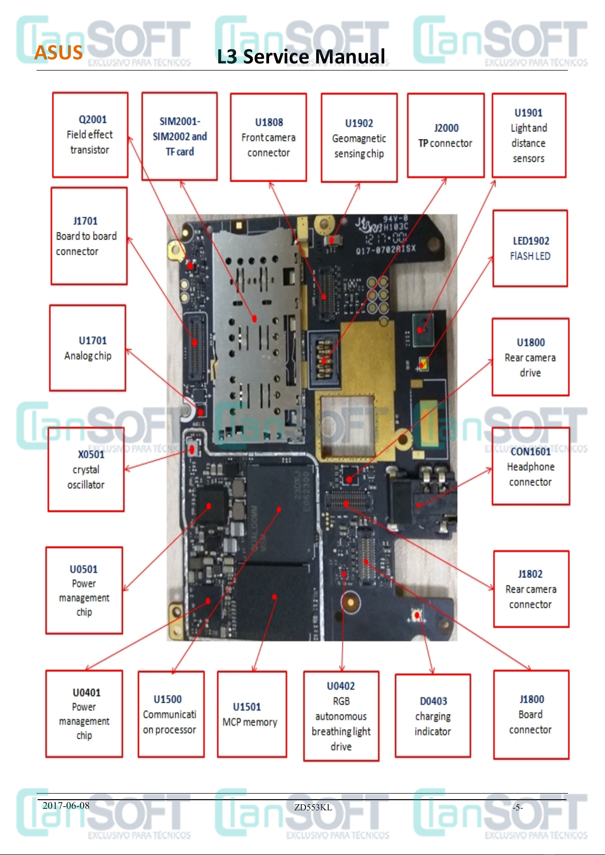
1. ZD553KL Motherboard PCBA diagram
……………………………………………………………….…………………………………4
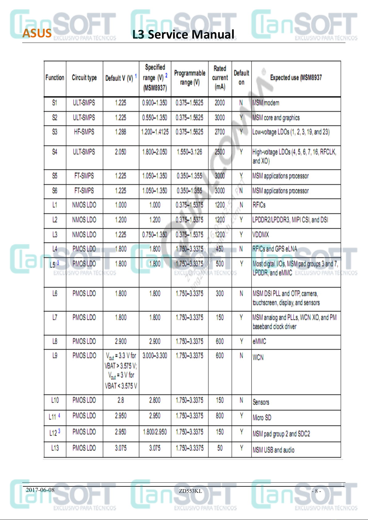
2. Main chip work principle…………..……………………..…………………………………………………………………………………..7
三: Common Fault Analysis
1.Boot class fault……….………………………………………………………………………………………………………………..…………12
2.Display class fault…………………………….……………………………………………………………………………………….…………16
3.Sound class fault………………………………………………………………….……………………………………………………………...19
4. Touch screen fault………………………..…………………………………………………………………………………………………….29
5. Charging fault…………………………..…………………………………………………………………………………………………………28
6. Motor fault……………………….…………………………………………………………………………….……………………….…………33
7. SIM/UIM/T Card identification fault…………………….…………………………………………………………………………….35
8. Camera type
failure………………………………….…………………………………………………………….…………………………..39
9.GPS/WIFI/BT failure……………………………………………………….……………………………………………………………………44
10.FM demodulation circuit
failure…………………………………….……………………………………………………………………47
11. Front and rear flash bad…………………………….………………………………………………………...……………………………50
12. Light distance sensor failure………………………………………………………………………………………..…………………….52
13.Gyrosensorfault …….……………………………………….………………………………………………………………………………….54
RF class failure( Refer to RF bad analysis)
Contents