AZZA PT-5IH User manual

PT-5IH
( VER. 1.x )
SYSTEM BOARD
OPERATION MANUAL

PT-5IH SYSTEM BOARD TABLE OF CONTENTS
TABLE OF CONTENTS
Chapter & Section Page
1. INTRODUCTION 1-1
1.1 SYSTEM OVERVIEW 1-1
1.2 FEATURES 1-1
2. SPECIFICATIONS 2-1
3. SYSTEM BOARD LAYOUT 3-1
3.1 5IH (VER. 1.x) 3-1
4. HARDWARE SETUP 4-1
4.1 UNPACKING 4-1
4.2 HARDWARE CONFIGURATION 4-1
4.2.1 DRAM INSTALLATION 4-1
4.2.2 L2 CACHE MEMORY INSTALLATION 4-3
4.2.3 CONNECTORS 4-4
4.2.4 JUMPERS 4-7
5. AWARD BIOS SETUP 5-1
5.1 GETTING STARDED 5-1
5.2 MAIN MENU 5-2
5.3 CONTROL KEYS 5-2
5.4 STANDARD CMOS SETUP 5-3
5.5 BIOS FEATURES SETUP 5-4
5.6 CHIPSET FEATURES SETUP 5-5
5.7 POWER MANAGEMENT SETUP 5-6
5.8 PNP/PCI CONFIGURATION 5-7
5.9 INTEGRATED PERIPHERALS 5-9
THE OTHER SETUPS 5-10
i

PT-5IH SYSTEM BOARD
TRADEMARKS
All trademarks used in this manual are the property of their respective owners.
NOTE
The "LOAD SETUP DEFAULTS" function loads the default settings directly from
BIOS default table, these default settings are the best-case values that should optimize
system performance. This function will be necessary when you accept this system
board, or the system CMOS data is corrupted.
By pressing "Enter" key, while "LOAD SETUP DEFAULTS" is highlighted, then
presses "Y" and "Enter" key. the SETUP default values will be loaded. (Please refer to
the Chapter 5 AWARD BIOS SETUP procedures in this maulal.)
NOTICE
Information presented in this manual has been carefully checked for reliability;
however, no responsibility is assumed for inaccuracies. The information contained in
this manual is subject to change without notice.
ii

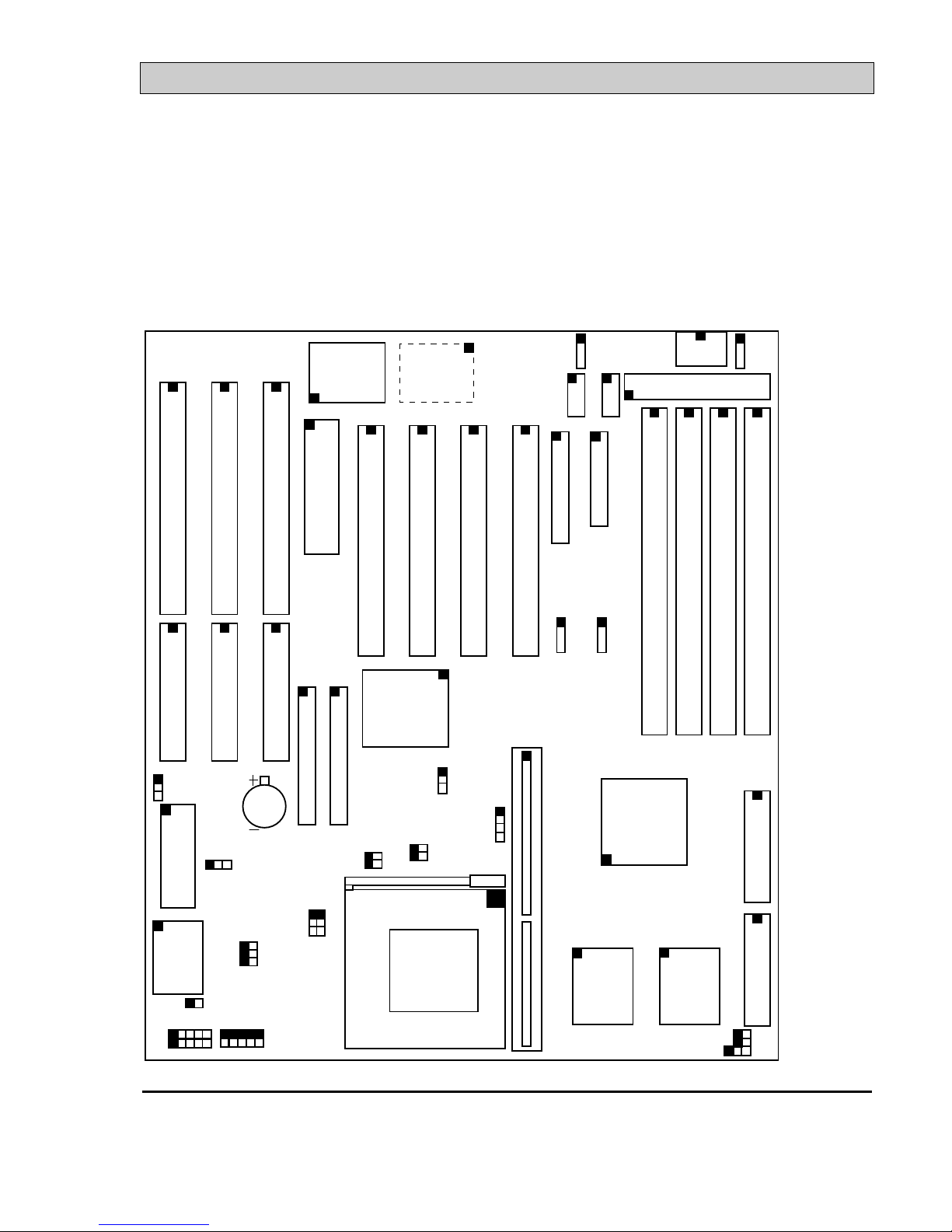
PT-5IH SYSTEM BOARD INTRODUCTION
1. INTRODUCTION
1.1 SYSTEM OVERVIEW
ThePT-5IHPentium PCI Local Bus system board is designed based on the Intel 82430HX PCIset system
chipset and Winbond (or SMC, UMC) I/O chipset, which built-in two channels PIO and Bus Master Enhanced
PCI IDE port, one Floppy Disk control port, two high speed Serial ports (UARTs) and one multimode Parallel
prot and also supports IR and USB ports. It is designed to fit a high performance, Pentium 75 MHz to 200 MHz
(ideally) based solution for high-end and true GREEN-PC computer systems.
This system board supports the Peripheral Component Interconnect (PCI) Local Bus standard (PCI Spec. Rev.
2.1 compliant). It not only breaks through the I/O bottlenecks of the traditional ISA main board, but also
provides the performance needs for networking and multi-user environments.
1.2 FEATURES
The PT-5IH system board contains the following features:
Pentium P54C/P54CT/P54CS/P55C, Cyrix 6x86 & AMD 5k86 based, PC/AT compatible
system board with ISA Bus and PCI Local Bus.
Supports the most part of "586" level CPUs designed by Intel, Cyrix and AMD.
Built-in 2 sets voltage regulator circuit to support multi-spec. CPU I/O voltage (includes
Standard, VR and VRE specification) and CPU CORE voltage (+2.5V DC and +2.8V DC).
DRAM Memory : Supports both fast page mode (FPM) and Extended Data Out (EDO).
Supports memory Parity or ECC (optional)
Cache Memory : Supports pipelined burst SRAMs. Cacheability main memory size up to
512MB.
BIOS : Supports Plug and Play BIOS.
IDE ports : Supports two channels PIO and Bus Master Enhanced PCI IDE port, up
to Mode 4 timing, and up to 22 MBytes/s transfer rates.
I/O ports : Supports two high speed serial ports (UARTs), One multimode parallel
port for standard (SPP), enhanced (EPP) and high speed (ECP) modes.
One Floppy Disk Control port.
IR Port (option) : Supports IR (Infrared Rays) functions. Both HPSIR and ASKIR are
supported.
USB Ports : Supports two Universal Serial Bus (USB) ports. (in the future)
Software : MS-DOS, WindowsNT, OS2, XENIX, UNIX, NOVELL, CAD/CAM,
compatibility Windows, Windows 95....etc.
1-1

PT-5IH SYSTEM BOARD SPECIFICATIONS
2. SPECIFICATIONS
CPU
Intel : Pentium processor and OverDrive processor (P54C/P54CS/P54CT/P55C/P55CT)
75/90/100/120/133/150/166 MHz and 180/200 MHz. (ideally)
Cyrix : 6x86-P120+(100MHz) / P133+(110MHz) / P150+(120MHz) / P166+(133MHz).
AMD : 5k86-P75(SSA/5-66)/ P75(SSA/5-75)/ P90(SSA/5-83)/ P90(SSA/5-90)/ P100(SSA/5-100)
CPU VCC
(1). CPU I/O voltage : Supports Standard, VR and VRE specification.
(2). CPU CORE voltage : Supports "egual to CPU I/O voltage", "+2.5V " and "+2.8V" DC
WORD SIZE
Data Path : 8-bit, 16-bit, 32-bit, 64-bit
PC System Chipset
Intel 82430HX PCIset (82439HX, 82371SB)
I/O Chipset
Winbond W83877F (or SMC FDC37C669 or UMC UM8669F).
System Clock
50/55/60/66.6 MHz adjustable.
Memory
DRAM : Two banks, each bank could be single or double sided, 8MB up to 256 MB.
Supports both fast page mode (FPM) and Extended Data Out (EDO) memory
(Using 72-pin SIMM module). 8 Qword deep merging DRAM write buffer.
Optional Parity or ECC (Error Checking and Correction).
SRAM : Two banks, 256/512KB Direct-Mapped wirte back cache memory, supports on-
board 256KB or 512KB pipelined burst SRAM. One SRAM Module Slot for
upgrading to 512KB. Cacheability main memory size up to 512 MB.
BIOS
AWARD or AMI System BIOS. 128KBx8, Flash ROM. (Plug & Play BIOS)
Expansion Slots
PCI Slots : 32-bit x 4 (All Master/Slave, PCI Spec. Rev. 2.1 Compliant)
ISA Slots : 16-bit x3
IDE Ports
Two channels PIO and Bus Master PCI IDE port, maximum could be connected 4 IDE Hard
Disk and ATAPI CD-ROM device.
2-1

PT-5IH SYSTEM BOARD SPECIFICATIONS
Super I/O Ports
1. Two high speed NS16C550 compatible serial prots (UARTs).
2. One parallel port, supports SPP/EPP/ECP mode.
3. One Floppy Disk Control port.
IR Port (option)
One HPSIR and ASKIR compatible IR transmission connector (5-pin).
Mouse and Keyboard
Supports PS/2 mouse connector, PS/2 keyboard connector (option) and AT keyboard connector.
USB Ports (in the future)
Two Universal Serial Bus (USB) ports.
DIMENSION
Width & Length : 220 mm x 270 mm.
Height : 3/4 inches with components mounted, but without expansion
boards and cables.
PCB Thickness : 4 layers, 0.05 inches normal.
Weight : 20.5 ounces.
ENVIRONMENT
Operating Temperature : 10*C to 40*C. (50*F to 104*F)
Required Airflow : 50 linear feet per minute across 80486 CPU.
Storage Temperature : - 40*C to 70*C. (- 40*F to 158*F)
Humidity : 0 to 90% noncondensing.
Altitude : 0 to 10,000 feet.
2-2

PT-5IH SYSTEM BOARD SYSTEM BOARD LAYOUT
3. SYSTEM BOARD LAYOUT
3.1 PT-5IH Ver. 1.x
Explanation : All connectors, jumpers and components which marks by a black point on the corner
means the pin-1 side of the connector, jumper and component.
K/B BIOS
Winbond
W83877F
PCI 1
PCI 2
PCI 3
SL2
CN1 POWER CON.
CN3
AT K/B
SIMM 1
SIMM 2
SIMM 3
SIMM 4
Intel
82371SB
Intel
82439HX
BAT 1
CPU
SYS. BIOS
CN12 IDE1
CN13 IDE2
CN8 FDC
CN4 LPT
COM B
CN7
J1
PS/2
MS.
CN5
IR
JP17
CN9
U4/U3 TAG 1
SPEAKER
KEYLOCK
HLTL
SSTS
RS
SMC/UMC
669
PCI 4
SL1
SL3
JP16
JP11
JP12
RTC
MODULE
Socket 7
CN6
COM A
U7 U5
Pipeline
Burst
SRAM
32K/64K
Pipeline
Burst
SRAM
32K/64K
*32
*32
U2/U1 TAG 0
CN11
PBSRAM MODULE
JP5
JP4
JP13
JP14
JP15
JP18
JP1
JP2
JP3
CN10
USB 2 USB 1
JP6
JP7
JP8
JP9
3-1

PT-5IH SYSTEM BOARD HARDWARE SETUP
4. HARDWARE SETUP
4.1 UNPACKING
The system board package should contain the following parts :
The PT-5IH system board.
OPERATION MANUAL.
Cable set for IDE and I/O device.
4.2 HARDWARE CONFIGURATION
Before the system board is ready to operate, the hardware must be configured to allow for various functions
within the system. To configure the PT-5IH system board is a simple task, only a few jumpers, connectors,
cables and sockets needs to be selected and installed. For the detailed locations of each component please refer
to the system board layout figure which appears in page 3-1.
4.2.1 DRAM INSTALLATION
The PT-5IH system board will support two banks main memory (bank0 and bank 1) on board, (using four 72-
Pin SIMM socket, SIMM 1 - 4), each bank could be single or double sided. With the use of 1MBx36(32)-S,
2MBx36(32)-D, 4MBx36(32)-S or 8MBx36(32)-D and 16MBx36(32)-S SIMM modules, 8MB up to 256 MB of
local memory can be attained. Both standard fast page mode (FPM) and Extended Data Out (EDO) memory are
supported, but they cannot be mixed within the same memory bank. The speed of FPM DRAMs must be used
70ns or faster than 70ns and the speed of EDO DRAMs must be used 60ns or faster than 60ns.
(Note : S = Single sided , D = Double sided)
There is no jumper needed for DRAM configuration, DRAMs' type and size will be detected by system BIOS
automatically.
In DRAM memory subsystem, ECC and Parity can be checked on the DRAM interface (selected by BIOS via
CMOS setup, please refer to Chapter 5). The defult status is parity selected. The DRAM SIMMs must be
populated with 72-bit wide memory (with parity bit) to implement ECC or Parity functions.
ECC is an optional data integrity feature provided by the system. This feature provides single-error correction,
double-error detection, and detection of all errors confined to single nibble for DRAM memory subsystem.
4-1

PT-5IH SYSTEM BOARD HARDWARE SETUP
The following table provides all possible DRAM memory combination.
Total Bank 0 Bank 1 Total Bank 0 Bank 1
Size SIMM1, SIMM2 SIMM3, SIMM4 Size SIMM1, SIMM2 SIMM3, SIMM4
8 MB 1MBx36(32)-S Empty 64 MB 8MBx36(32)-D Empty
16 MB 1MBx36(32)-S 1MBx36(32)-S 72 MB 8MBx36(32)-D 1MBx36(32)-S
24 MB 1MBx36(32)-S 2MBx36(32)-D 80 MB 8MBx36(32)-D 2MBx36(32)-D
40 MB 1MBx36(32)-S 4MBx36(32)-S 96 MB 8MBx36(32)-D 4MBx36(32)-S
72 MB 1MBx36(32)-S 8MBx36(32)-D 128 MB 8MBx36(32)-D 8MBx36(32)-D
136 MB 1MBx36(32)-S 16MBx36(32)-S 192 MB 8MBx36(32)-D 16MBx36(32)-S
16 MB 2MBx36(32)-D Empty 128 MB 16MBx36(32)-S Empty
24 MB 2MBx36(32)-D 1MBx36(32)-S 136 MB 16MBx36(32)-S 1MBx36(32)-S
32 MB 2MBx36(32)-D 2MBx36(32)-D 144 MB 16MBx36(32)-S 2MBx36(32)-D
48 MB 2MBx36(32)-D 4MBx36(32)-S 160 MB 16MBx36(32)-S 4MBx36(32)-S
80 MB 2MBx36(32)-D 8MBx36(32)-D 192 MB 16MBx36(32)-S 8MBx36(32)-D
144 MB 2MBx36(32)-D 16MBx36(32)-S 256 MB 16MBx36(32)-S 16MBx36(32)-S
32 MB 4MBx36(32)-S Empty
40 MB 4MBx36(32)-S 1MBx36(32)-S (Note : S = Single sided , D = Double sided)
48 MB 4MBx36(32)-S 2MBx36(32)-D
64 MB 4MBx36(32)-S 4MBx36(32)-S
96 MB 4MBx36(32)-S 8MBx36(32)-D
160 MB 4MBx36(32)-S 16MBx36(32)-S
4-2

PT-5IH SYSTEM BOARD HARDWARE SETUP
4.2.2 L2 CACHE MEMORY INSTALLATION
The PT-5IH system board will support one or two bank(s) direct-mapped second level cache and provides either
256KB or 512KB cache memory using synchronous pipeline-burst SRAMs. (Note that this system board does
not support asynchronous or burst SRAMs for the cache memory) Both Write Back and Write Through cache
update policy are supported.
If the on-board cache memory size is 256KB, a COAST (Cache-On-A-STick) module (256KB) will be use for
upgrade the cache memory size from 256KB to 512KB. There is no jumper needed for end-user while upgrade
cache memory size, just insert the COAST module into the SRAM module slot (CN11), then the cache memory
size will be detected by system BIOS automatically.
Note : The COAST modules design must comply with Intel COAST (Cache-On-A-STick)
module specification revision 2.0 or later.
The following table lists the detalied combination about cache memory installation.
Cache Data SRAMs Tag SRAMs COAST
Size U5 ,U7 U2 (or U1) U4 (or U3) SRAM module
(optional) (CN11)
256 KB 32KB x 32 8KB or 16KB or 32KB x 8 8KB or 16KB or 32KB x 8Empty
512 KB 32KB x 32 8KB or 16KB or 32KB x 8 8KB or 16KB or 32KB x 8256 KB
512 KB 64KB x 32 16KB or 32KB x 8 16KB or 32KB x 8Empty
This system board supports the memory space cacheability limit for the second level cache is 64MB of main
memory base, and also supports an optional extended memory space cacheability limit of 512MB, but for this
feature an additional Tag SRAM ( TAG1, U4 or U3) is needed. (Note that the specification of the additional
Tag SRAM must same as TAG 0 ). Insert a SRAM into TAG1, then execute the CMOS setup procedure change
the "L2 Cache Cacheable Size" item (in the CHIPSET FEATURE SETUP) from 64MB to 512 MB. (Please
refer to Chapter 5)
The following table shows the sizes and quantities of Tag SRAM needed to support different memory sizes of
cacheability.
Cache Size TAG Size Memory size of
TAG 0 (U2 or U1) TAG 1 (U4 or U3) Cacheability
256 KB 8KB or 16KB or 32KB x 8Empty 64 MB
256 KB 8KB or 16KB or 32KB x 8 8KB or 16KB or 32KB x 8512 MB
512 KB 16KB or 32KB x 8Empty 64 MB
512 KB 16KB or 32KB x 8 16KB or 32KB x 8 512 MB
4-3

PT-5IH SYSTEM BOARD HARDWARE SETUP
4.2.3 CONNECTORS
A connector is two or more pins that are used make connections to the system standard accessories (such as
power, mouse, printer,...etc.) The following is a list of connectors on board, as well as descriptions of each
individual connector.
(A) BAT1 Non-Rechargeable battery (Using 3 Vlots Lithium battery : CR2032)
Pin # Assignment
Battery Positive
Ground
(B) CN1 Power connector
Pin # Assignment Pin # Assignment Pin # Assignment
1 Power Good 5 Ground 9 -5V DC
2 +5V DC 6 Ground 10 +5V DC
3 +12V DC 7 Ground 11 +5V DC
4 -12V DC 8 Ground 12 +5V DC
(C) CN2 PS/2 Keyboard connector (option)
Pin # Assignment Pin # Assignment Pin # Assignment
1 Keyboard Data 3 Ground 5 Keyboard Clock
2 No Connection 4 +5V DC 6 No Connection
(D) CN3 AT Keyboard connector
Pin # Assignment Pin # Assignment Pin # Assignment
1 Keyboard Clock 3 No Connection 5 +5V DC
2 Keyboard Data 4 Ground
(E) CN4 Parallel Port connector
(Supports SPP/EPP/ECP mode, selected by BIOS setup,using IRQ7 or IRQ5,
ECP using DMA channel 3 or 1)
114 Pin# Assignment Pin # Assignment
1 STROBE- 14 AUTO FEED-
2 Data Bit 0 15 ERROR-
3 Data Bit 1 16 INIT-
4 Data Bit 2 17 SLCT IN-
5 Data Bit 3 18 Ground
6 Data Bit 4 19 Ground
7 Data Bit 5 20 Ground
8 Data Bit 6 21 Ground
9 Data Bit 7 22 Ground
10 ACK- 23 Ground
11 BUSY 24 Ground
12 PE 25 Ground
13 SLCT 26 N.C. (No Connection)
13 26
4-4

PT-5IH SYSTEM BOARD HARDWARE SETUP
(F) CN5 IR (Infrared Rays) transmission connector
Pin # Assignment Pin # Assignment Pin # Assignment
1 +5V DC 3 IR Receive 5 IR Transmit
2 No Connection 4 Ground
(G) CN6 COM B (Serial Port 2) connector
COM1/2/3/4, selected by BIOS setup, using IRQ3 or 4
1 2 Pin # Assignment Pin # Assignment
1 DCD (Data Carrier Detect) 2 RD (Received Data)
3 TD (Transmit Data) 4 DTR (Data Terminal Ready)
5 Ground 6 DSR (Data Set Ready)
7 RTS (Request To Send) 8 CTS (Clear To Send)
9 RI (Ring Indicator) 10 NC (No Connection)
910
(H) CN7 COM A (Serial Port 1) connector
COM1/2/3/4, selected by BIOS setup, using IRQ4 or 3
1 2 Pin # Assignment Pin # Assignment
1 DCD (Data Carrier Detect) 2 RD (Received Data)
3 TD (Transmit Data) 4 DTR (Data Terminal Ready)
5 Ground 6 DSR (Data Set Ready)
7 RTS (Request To Send) 8 CTS (Clear To Send)
9 RI (Ring Indicator) 10 NC (No Connection)
910
(I) CN8 Floppy Disk Control Port connector (Using IRQ6, DMA channel 2)
(J) CN9 USB (Universal Serial Bus) port1 connector
(K) CN10 USB (Universal Serial Bus) port2 connector
(L) CN11 Pipeline-burst SRAM (COAST) module slot
(M) CN12 IDE 1 connector (Primary IDE Port, using IRQ14)
(N) CN13 IDE 2 connector (Secondary IDE Port, using MIRQ0)
(O) J1 PS/2 Mouse converted connector
Pin # Assignment
1 Mouse Data
2 No Connection
3 Ground
4 +5V DC
5 Mouse Clock
4-5

PT-5IH SYSTEM BOARD HARDWARE SETUP
(P) RS Reset Button connector
Pin # Assignment Pin1&2 Function
1 Reset Control Open No action
2 Ground Short Reset
(Q) HL IDE HDD LED connector
Pin # Assignment
1 Pullup (+5V DC)
2 Signal Pin
(R) SS External SMI button connector
Pin # Assignment Pin1&2 Function
1 SMI Control Open For normal operation
2 Ground Short To get into Suspend mode
(S) TL Turbo LED connector
Pin # Assignment
1 Pullup (+5V DC)
2 Signal Pin
(T) TS Turbo Switch connector (This function is reserved)
Pin # Assignment Pin1&2 Function
1 Turbo Control Open Turbo
2 Ground Short Normal
(U) SPEAKER Speaker connector
Pin # Assignment Pin # Assignmen
1 +5V DC 4 Speaker Data Signal
2 No Connection 5 No Connection
3 No Connection
(V) KEY LOCK Front Panal Power LED & Key-Lock connector
Pin # Assignment Pin # Assignmen
1 Pullup (+5V DC) 4 Keyboard Lock
2 No Connection 5 Ground
3 Ground
Explanation : ( For next section : JUMPERS )
open
1-2
1
2-3
1
1
11
short
,
,
4-6
PT-5IH SYSTEM BOARD HARDWARE SETUP

4.2.4 JUMPERS
A jumper is two, three or more pins which may or may not be covered by a plastic connector plug (mini-
jumper). A jumper is used to select different system options. Please make sure all jumpers at correct position
before this system board used.
(A) JP6-JP9 CPU type selection
(1) INTEL Pentium / Pentium-MMX CPUs
CPU Type JP6 JP7 JP8 JP9 Remark
80502-75 short short open open
80502-90 open short open open
80502-100 short open open open
80502-120 open short short open
80502-133 short open short open
80502-150 open short short short
80502-166 / 80503-166 short open short short
80502-180 open short open short
80502-200 / 80503-200 short open open short
80503-233 short open open open
(2) Cyrix 6x86 / 6x86L CPUs
CPU Type JP6 JP7 JP8 JP9 Remark
6x86 / 6x86L -P120+ short short short open
6x86 / 6x86L -P133+ open open short open
6x86 / 6x86L -P150+ open short short open
6x86 / 6x86L -P166+ short open short open
(3) AMD K5 CPUs
CPU Type JP6 JP7 JP8 JP9 Remark
AMD-K5-PR75 short short open open
AMD-K5-PR90 open short open open
AMD-K5-PR100 short open open open
AMD-K5-PR120 open short open open
AMD-K5-PR133 short open open open
AMD-K5-PR150 open short short short
AMD-K5-PR166 short open short short
4-7

PT-5IH SYSTEM BOARD HARDWARE SETUP
(B) JP11-JP16, JP19 CPU operating voltage selection
Note : (1). For the detailed CPU-VCC requirement, please inquire of your CPU supplier.
(2). In PT-5IH VER.. 1.2 & VER. 1.3 , the JP19 is inexistent, you could skip it.
CPU VCC
I/O CORE JP11 JP12 JP13 JP14 JP15 JP16 JP19 Remark
voltage voltage
+ 3.3 V + 3.3 V 2-3 2-3 short open open x 2-3
+ 3.4 V + 3.4 V 2-3 2-3 open short open x 2-3 *
+ 3.5 V + 3.5 V 2-3 2-3 open open short x 2-3
+ 3.3 V + 2.5 V 1-2 1-2 short open open 1-2 1-2
+ 3.4 V + 2.5 V 1-2 1-2 open short open 1-2 1-2 **
+ 3.5 V + 2.5 V 1-2 1-2 open open short 1-2 1-2
+ 3.3 V + 2.8 V 1-2 1-2 short open open 2-3 1-2
+ 3.4 V + 2.8 V 1-2 1-2 open short open 2-3 1-2 ***
+ 3.5 V + 2.8 V 1-2 1-2 open open short 2-3 1-2
Remark :
x : Don't care
* : For the single-VCC required CPUs. (e.g. Intel P54C, Cyrix 6x86, AMD-SSA/5-xxAB?,
AMD-SSA/5-xxAC?, AMD-SSA/5-xxAF? ... etc.)
** : For a part of the dual-VCC required CPUs.
(e.g. Intel P55C-166, Cyrix M2, AMD-SSA/5-xxAK? ... etc.)
*** : For a part of the dual-VCC required CPUs.
(e.g. Intel P55C-200, Cyrix M2, AMD-SSA/5-xxAH?, AMD-SSA/5-xxAJ? ... etc.)
(C) JP17 ROM BIOS Selection
Pin # Function
1-2 For +5V FLASH ROM, EPROM
2-3 For +12V FLASH ROM
(D) JP18 Clear CMOS button
Pin # Function
open Normal operation
short Clear CMOS (Note : Don't forget to open this jumper after 2-3 seconds)
Note : Depends on different brand-name of RTC IC (U27 or U28), there are two times
to clear CMOS, the following is a list for reference :
(1) while power-on : BENCHMARQ / bq3287AMT, SGS / M48T86,
(2) while power-off : VIA / VT82885N, ODIN / OEC12C885 / OEC12C887A,
DALLAS / DS12887A.
(E) JP1-JP5 (Reserved)
4-8

PT-5IH SYSTEM BOARD AWARD BIOS SETUP
5. AWARD BIOS SETUP
5.1 GETTING STARTED
When the system is first powered on or reset, the BIOS will enter the Power-On Self Test routines ( POST :
Display a copyright message on the screen followed by a diagnostics and initialization procedure.) (If an EGA
or VGA card is installed, the copyright message of the video card maybe displayed on the screen first.) The
BIOS will indicate any error or malfunction by a series of beeps or display the error message on screen.
Normally, the simulate figure 5-1 will display on the screen when the system is powered on.
Fig. 5-1 Initial Power-On screen.
After the POST routines are completed, the following message appears :
" Press DEL to enter SETUP "
To execute the Award BIOS Setup program, press DEL key. The simulate screen in figure 5-2 MAIN MENU
will be displayed at this time.
5-1

PT-5IH SYSTEM BOARD AWARD BIOS SETUP
5.2 MAIN MENU
ROM PCI / ISA BIOS (2A59FXXX)
CMOS SETUP UTILITY
AWARD SOFTWARE, INC.
STANDARD CMOS SETUP SUPERVISOR PASSWORD
BIOS FEATURES SETUP USER PASSWORD
CHIPSET FEATURES SETUP IDE HDD AUTO DETECTION
POWER MANAGEMENT SETUP HDD LOW LEVEL FORMAT
PNP/PCI CONFIGURATION SAVE & EXIT SETUP
INTEGRATED PERIPHERALS EXIT WITHOUT SAVING
LOAD SETUP DEFAULTS
ESC : Quit : Select Item
F10 : Save & Exit Setup (Shift)F2 : Change Color
Time, Date, Hard Disk Type ...
Fig. 5-2 CMOS SETUP MAIN MENU screen.
5.3 CONTROL KEYS
Listed below is an explanation of the keys displayed at the bottom of the screens accessed through the BIOS
SETUP program :
Arrow Keys : Use the arrow keys to move the cursor to the desired item.
Enter : To Select the desired item.
F1 : Display the help screen for the selected feature.
(Shift)F2 : To change the screen color, total 16 colors.
ESC : Exit to the previous screen.
PgUp(-)/PgDn(+) : To modify the default value of the options for the highlighted feature.
F5 : Retrieves the previous CMOS values from CMOS, only for the current option
page setup menu.
F6 : Loads the BIOS default values from BIOS default table, only for the current
option page setup menu.
F7 : Loads the SETUP default values from BIOS default table, only for the current
option page setup menu.
F10 : Save all changes made to CMOS RAM, only for the MAIN MENU.
5-2

PT-5IH SYSTEM BOARD AWARD BIOS SETUP
The following pages will show the simulate screens of CMOS SETUP, each figure contains the setup items and
the default settings of them. Below each figure may or may not be contained a lists of function description for
commonly used settings. For the other settings' function description you needed, connet to us please.
5.4 STANDARD CMOS SETUP
ROM PCI / ISA BIOS (2A59FXXX)
STANDARD CMOS SETUP
AWARD SOFTWARE, INC.
Date (mm : dd : yy) : Thu, May 11 1996
Time (hh : mm : ss) : 9 : 53 : 54
HARD DISKS TYPE SIZE CYLS HEAD PRECOMP LANDZ SECTOR MODE
Primary Master Auto 0 0 0 0 0 0 Auto
Primary Slave Auto 0 0 0 0 0 0 Auto
Secondary Master Auto 0 0 0 0 0 0 Auto
Secondary Slave Auto 0 0 0 0 0 0 Auto
Drive A : 1.44M, 3.5 in.
Drive B : None Base Memory : 640 K
Extended Memory : xxxxxx K
Video : EGA/VGA Other Memory : xxxxxx K
Halt On : All Errors Total Memory : xxxxxx K
ESC : Quit : Select Item PU/PD/+/- : Modify
F1 : Help (Shift)F2 : Change Color
Fig. 5-3 STANDARD CMOS SETUP screen.
MODE :
For IDE hard disks, this BIOS provides three modes to support both normal size IDE hard disks and also disks
size larger the 528MB:
NORMAL : For IDE hard disks size smaller then 528MB.
LBA : For IDE hard disks size larger then 528MB and up to 8.4GB (Giga Bytes) that use
Logic Block Addressing (LBA) mode.
Large : For IDE hard disks size larger then 528MB that do not use LBA mode.Large mode
is a new specifition which may not be fully supported by all operation systems.
Now it can only be used with the MS-DOS and is uncommon.
Note : Some OSes (like SCO-UNIX) must use "NORMAL" for installation.
5-3

PT-5IH SYSTEM BOARD AWARD BIOS SETUP
5.5 BIOS FEATURES SETUP
ROM PCI / ISA BIOS (2A59FXXX)
BIOS FEATURES SETUP
AWARD SOFTWARE, INC.
Virus Warning : Disabled Video BIOS Shadow : Enabled
CPU Internal Cache : Enabled C8000-CBFFF Shadow : Disabled
External Cache : Enabled CC000-CFFFF Shadow : Disabled
Quick Power On Self Test : Enabled D0000-D3FFF Shadow : Disabled
Boot Sequence : A, C D4000-D7FFF Shadow : Disabled
Swap Floppy Drive : Disabled D8000-DBFFF Shadow : Disabled
Boot Up Floppy Seek : Enabled DC000-DFFFF Shadow : Disabled
Boot Up NumLock Status : On
Boot Up System Speed : High
Gate A20 Option : Fast
Typematic Rate Setting : Disabled
Typematic Rate (Chars/Sec) : 6
Typematic Delay (Msec) : 250
ESC : Quit : Select Item
Security Option : Setup F1 : Help PU/PD/+/- : Modify
PCI/VGA Palette Snoop : Disabled F5 : Old Values (Shift)F2 : Color
OS Select For DRAM > 64MB : Non-OS2 F6 : Load BIOS Default
F7 : Load Setup Default
Fig. 5-4 BIOS FEATURES SETUP screen.
Virus Warning :
This feature flashes on the screen. During and after the system boots up, any attempt to write to the boot sector
or partition table of the hard disk drive will halt the system and an error message will appear, in the mean time,
you can run anti-virus program to locate the problem. Default values is "Disabled"
Enabled : Activate automatically when the system boots up causing a warning message to appear
when anything attempts to access the boot sector or hard disk partition table.
Disabled : No warning message to appear when anything attempts to access the boot sector or hard
disk partition table.
CPU Internal Cache :
This option enables CPU's internal (L1) cache memory. If you want to use the internal (L1) cache memory and
external (L2) cache memory, this option must be enabled.
External Cache :
This option enables L2 (secondary) external cache memory. If none external cache memory on board you must
set this option to "disabled", otherwise, you can select enabled or disabled.
5-4

PT-5IH SYSTEM BOARD AWARD BIOS SETUP
5.6 CHIPSET FEATURES SETUP
ROM PCI / ISA BIOS (2A59FXXX)
CHIPSET FEATURES SETUP
AWARD SOFTWARE, INC.
Auto Configuration : Enabled DRAM ECC/PARITY Select : Parity
DRAM Timing : 70 ns Memory Parity/ECC Check : Disable
DRAM RAS# Precharge Time : 4 Single Bit Error Report : Enabled
DRAM R/W Leadoff Timing : 7/6 L2 Cache Cacheable Size : 64MB
DRAM RAS to CAS Delay : 3 Pipeline Cache Timing : Faster
DRAM Read Burst (EDO/FPM) : x333/x444
DRAM Write Burst Timing : x333
Turbo Read Leadoff : Disabled
DRAM Speculative Leadoff : Disabled
Turn-Around Insertion : Disabled
ISA Clock : PCICLK/4
System BIOS Cacheable : Disabled
Video BIOS Cacheable : Disabled
8 Bit I/O Recovery Time : 1
16 Bit I/O Recovery Time : 1 ESC : Quit : Select Item
Memory Hole At 15M-16M : Disabled F1 : Help PU/PD/+/- : Modify
Peer Concurrency : Enabled F5 : Old Values (Shift)F2 : Color
F6 : Load BIOS Default
F7 : Load Setup Default
Fig. 5-5 CHIPSET FEATURES SETUP screen.
WARNING : The CHIPSET FEATURES SETUP in this screen are provided so that technical
professionals can modify the Chipset to suit their requirement. If you are not a
technical engineer, do not use this program !
Auto Configuration :
When "Enabled", this parameter automatically enters and locks some of the optimum values for the chipset and
CPU. Otherwise, this parameter allows the values of these parameters could be changed.
DRAM Timing :
When "Auto Configuration" is "Enabled", this parameter provides two suit of the optimum values for the chipset
and CPU, depends on the DRAMs' speed, you can select "70 ns" or "60 ns", but the first value maybe caused
your system more stable.
DRAM ECC/PARITY Select / Memory Parity/ECC Check / Single Bit Error Report :
Please refer to page 4-1 for the rough description.
L2 Cache Cacheable Size :
Please refer to page 4-3 for the detailed description.
5-5
Table of contents
Other AZZA Motherboard manuals