440E/LX AT MAINBOARD INTRODUCTION
1-1
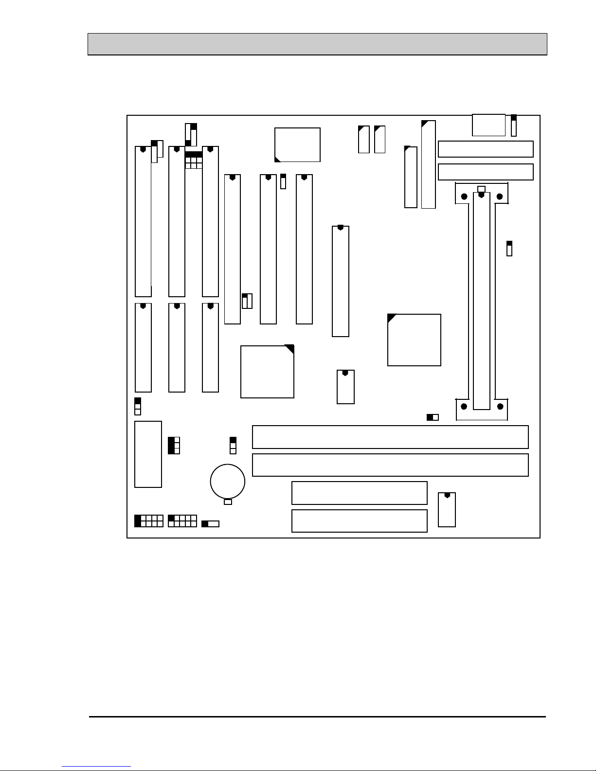
1. INTRODUCTION
1.1 OVERVIEW
This Mainboard is a high performance Pentium™ II personal computer mainboard with
66MHz ultra high Front Side Bus (FSB) frequency. It is an AT form-factor mainboard
with A.G.P. (Accelerated Graphics Port) and PCI Local Bus on board, Designed based
on the Intel® 82440EX or 82440LX AGPset™ system chipset.
When the 440LX chipset is installed on the board, it will be the PentiumTM II LX
mainboard. When the chipset on the mainboard is 440EX, it will become PentiumTM II
EX mainboard. The difference between LX and EX on this mainboard is LX mainboard
supports ECC feature in the memory subsystem, while EX board doesn’t.
The Winbond® I/O chipset is built on the board and it has built-in two channel “PIO”
and “Ultra DMA/33 Bus Master” mode PCI IDE ports, one Floppy Disk control port,
two high speed Serial ports (UARTs) and one multi-mode Parallel port and supports
PS/2™ mouse, IR and USB ports. It is designed to fit a high performance Pentium™ II
or Celeron™ processor 233 MHz, 266 MHz, 300 MHz, 333MHz and up to 366MHz
based solution for high-end and true GREEN-PC computer systems.
The Pentium™ II or Celeron™ Processor is a 64-bit processor with RISC technology,
which offers several key features such as built-in 128/256KB/512KB L2 cache (some
Celeron does not have L2 cache), 12-stage super-pipeline architecture, out of order
execution .... etc. In order to optimize of its performances, the 32-bit Operating System
(such as Windows® NT and OS/2™) and 32-bit applications are recommended.
The Accelerated Graphics Port (A.G.P.) on the mainboard is designed for AGP 3D
video display card. Unlike PCI-based display cards, the AGP technology provides
lightning data throughput to fully facilitate the 3-Dimensional and multimedia graphics
display. The data transfer rate on AGP can be up to 133Mhz and which is much faster
than the traditional 33MHz PCI VGA card.
The AGP is a new video display technology and it requires device driver or new
Operating System to enable this accelerated graphic feature. Windows® 98 supports
AGP directly but Windows® 95 still need the appropriate device drivers to support
AGP feature. Please don’t worry about the device driver, because you can always find
the device driver included in the AGP card.