Denon UD-M31 User manual

SERVICE MANUAL
MODEL
UD-M31
STEREO CD RECEIVER
Some illustrations using in this service manual are slightly different from the actual set.
16-11, YUSHIMA 3-CHOME, BUNKYOU-KU, TOKYO 113-0034 JAPAN
Telephone: 03 (3837) 5321
X0164V.02 DE/CDM 0302
For Europe & U.K. model
Version 2

2
2UD-M31
DISASSEMBLY
(Follow the procedure below in reverse order when reassembling)
1. TOP COVER
(1) Remove 2screws ①on both sides.
(2) Remove 5screws ②on the rear.
(3) Detach the Top Cover to the arrow direction.
2. FRONT PANEL
(1) Disconnect FFC on thr rear of the CD
Mecha.
(2) Remove 4 lower screws ③
(3) Detach the Front Panel with releasing the
hooks on both sides.
3. CD MECHANISM UNIT
(1) Disconnect FFC coming from the top of the
CD Mecha.
(2) Unplug the connector on fhe rear of the
µcom PWB .
(3) Unplug the connector on the I/O PWB.
(4) Remove 4 screws ④on the µcom PWB .
(5) Fully pull out the loader by turning the gear
under the loader of the CD Mecha.
(6) Remove 4 screws ⑤to detach the CD
Mecha.
SAFETY PRECAUTIONS
The following check should be performed for the continued protection of the customer and service technician.
LEAKAGE CURRENT CHECK
Before returning the unit to the customer, make sure you make either (1) a leakage current check or (2) a line to chassis
resistance check. If the leakage current exceeds 0.5 milliamps, or if the resistance from chassis to either side of the
power cord is less than 460 kohms, the unit is defective.
Top cover
FFC
CD Mecha.
Front Panel
Hook
Gear
Loader
FFC
Connector
I/O P.W.B.
µcon P.W.B.

3
3UD-M31
4. REAR PANEL
(1) Pull out the cord bush.
(2) Remove 12 screws ⑥
5. MAIN PWB
(1) Remove 4 screws ⑦fixing the radiator the chas-
sis.
(2) Unplug 3 connectors on the AMP PWB.
(3) Detach the Main PWB together with the radiator .
(4) Remove 5 screws ⑧.
(5) Detach the Power PWB.
6. DISPLAY PWB
(1) Pull out the VR knob.
(2) Remove the spacer and the VR nut ⑨.
(3) Remove 7 screws ⑩.
Cord Bush
Connector
Radiator
Power
P.W.B.
Main P.W.B.
VR knob

4
4
UD-M31
BLOCK DIAGRAM
TUNER MODULE
CD
MECHA
CD11FTA3N
IC801
LA6559
DRIVER
IC303
LC72720NM
RDS(E2/EK only)
IC802
LA9241
RF AMP
IC401
LC75725E
FL DRIVER
IC803
LC78625E
CD DSP
IC805
BA6287F
IC804
BA4510F
IC301
BU4066BCF
REC OUT SEL
IC302
LC75432M
SELECTOR & VR & EQ
IC305
BA15218F
IC304
BA15218F
IC205
M51957
IC201
UPD784216
MICON
IC501
STK402-050
POWER AMP
REC out
IN
REC out
Pre out
IN
IC202
93LC66
IC203
BA05ST
IC402
RPM6938
FL401
FL TUBE
TACT SW & VR ENCORDER
POWER
TRANS
RL602
POWER
RELAY
IC605
NJM7805F
Protection
TR501∼
RL601
SP
RELAY SP
OUT
SUB
TRANS
P.DOWM
TR607
IC603
NJM
7812FA
IC604
NJM
7806FA
IC602
NJM
7805FA
DENON
BUS
TR601∼603
AC IN

5
5
UD-M31
LEVEL DIAGRAM
CD
UNIT
TU
UNIT
0dB=0.55V
FUNCTION SWITCH
LINE 1
LINE 2
LINE 1
REC
LINE 2
REC
+4dB
ANALOG
SWITCH 4066
PRE OUT
+16dB
BUFFER BUFFER
MASTER VOLUME
MUTE
LC75342M
ATT HP
0dB play back CD=1.1V
LINE:1kHZ,150mV
EQ:FLAT
SDB:OFF
+0.83dB
0dB
-10dB
-104dB
(dBV)
-16.4dB
POWER AMPTONE/SDB
RELAY SP
(+6dB)
87.6dB
TOTAL 36dB
(+30dB)
15W/6
9.49V

6
6UD-M31
CD TEST MODE
Setting of the test mode and explanation of each button
* Laser light of the pickup is always emitted regardless of DISC loading in the test mode.
You may lose your eyesight if you look into the laser directly.
So be careful enough when operating in the test mode.
ITEM OPERATION FUNCTION DISPLAY
1 Start the mode Plug the AC cord to the wall outlet while push-
ing the POWER button and the Function button
1.This service mode starts
2.Pick up moves to the 10mm
position.
1.Display "01"
2.The PLAY and the PAUSE
mark lit
2 Disc load
1.Push the OPEN/CLOSE button and the
LOADER open
2.Place the disc and push the OPEN/CLOSE
button again
1.Load the CD disc
2.The pick up moves to the
10mm position
1.Display "01"
2.The PLAY and the PAUSE
mark lit
3Focus and Track-
ing check mode
1.Push the PLAY button
2.Push the PLAY button again
3.Push the PLAY button again
1.The laser ON
2.forcus servo on,the disc turns
3.Tracking servo and Slide
servo on
1.Display "02 L on"
2.Display"03 Fon"
3.Display "04 t on"
4 Move pick up 1.Push the SKIP forward button or the SKIP
reverse button while stopping
The pick up move forward or
reverse 1.Display "5 O PU"
5 Stop move Push the STOP button Stop the movement 1.Display "01"
6 All Servo on Push the SKIP button All servo on, and auto adjust
1.Display "06 Adj."
1.after auto adjust,d
display "01"
7 Clear this mode Unplug the AC cord
TD VCC VREF
FE
FD
RF
TE
1U-3507
CD UNIT

7
7UD-M31
FE
TE
TE
RF
FE
TE
RI
DRF
RFA (A=1.5±0.3Vp-p)
FE
TB
SLD
How to check the test mode
( 1 ) DISC discrimination, adjustment
* Insert DISC, and press the AUTO SEARCH REVERSE button.
* “06 Adj” is displayed, and discrimination of DISC size 8 cm/12 cm, discrimination of DISC reflectance (CD, CD-
R/CD-RW), adjustment of focus, tracking offset, and EF balance will be performed. (Adjusted values are not
displayed: Refer to Fig. 2, 3)
* After completing the discrimination and adjustment, it becomes stop condition.
* Once discrimination of DISC has been carried out in the “06 Adj” mode, discrimination of size and reflectance is
no longer made, and only adjustment will be performed.
( 2 ) Checking of servo state
* Press the PLAY button after performing above (1) “DISC discrimination, adjustment”.
* “02 L on” is displayed, and the laser will start to light. (The pickup may vibrate with a rattling noise if DISC has
been loaded, but this is not abnormal.)
* Press the PLAY button again.
* “03 F on” is displayed. DISC starts turning, and focus servo will be actuated. (Refer to Fig. 4, 5)
* Press the PLAY button again.
* “04 t on” is displayed. Tracking, CLV, and slide servo will be actuated.
* Monitor HF signal using the Test Point, HF point and VC point.
Check that the signal’s amplitude is 1.5V±0.3Vp-p. (Refer to Fig. 6)
Fig. 2 DISC discrimination,
adjustment (Case of CD-RW)
Fig. 3 Adjustment of EF balance
Fig. 4 In “03 F on” Fig. 5 In “03 F on”
Fig. 6 In “04 t on”

8
8UD-M31
WAVE-FORMS OF EACH POINT
SP
When 12 cm DISC
start
SP
When 8 cm DISC
start
SL
TE
Track search
(when forward)
SL
During PLAY
OPEN
CLOSE
When the tray
OPEN
SP
When 12 cm DISC
stop
SP
When 8 cm DISC
stop
TD
TE
RF
DRF
During PAUSE
SL
TE
Track search
(when reverse)
FD
Focus search
(no DISC)
FE
TE
DRF
RF
When focus
servo on

9
9UD-M31
SEMICONDUCTOR
IC’s
µPD784216AGC-8EU(IC201)
µPD784216AGC-8EU Terminal Function
Pin
No. Port Symbol I/O Function RECIEVER or CD outputs of
standby&Defoult
1 P120/RTP0 ENC A I Rotary encoder INPUT A RECIEVER -
2 P121/RTP1 ENC B I Rotary encoder INPUT B RECIEVER -
3 P122/RTP2 V.MUTE O Volume mute output, mute;High RECIEVER H
4 P123/RTP3 POWER O Amp circuit power ON/OFF output, ON:High RECIEVER L
5 P124/RTP4 /R.MUTE O Speaker Relay ON/OFF output, ON:High RECIEVER L
6 P125/RTP5 NC O Not used :NC OTHER L
7 P126/RTP6 SEL.EEPROM O EEPROM chip enable output RECIEVER L
8 P127/RTP7 FLCE O Chip select output to FL tube controller OTHER L
9 VDD VDD - Positive power OTHER -
10 X2 X2 - X'tal connection for main clock oscillation OTHER -
11 X1 X1 I X'tal connection for main clock oscillation OTHER -
12 VSS VSS - GND potential OTHER -
13 XT2 XT2 - x'tal connection for main sub-clock oscillation,
not used : :NC
14 XT1 XT1 I x'tal connection for main sub-clock oscillation,
not used :Connect to VSS orVCC
15 /RESET /RESET I Micro-computer reset input OTHER -
16 P00/INTP0 REMOCON I Remote-control receive data input RECIEVER -
17 P01/INTP1 50/60 I 50/60Hz AC input RECIEVER -
18 P02/INTP2/NMI /DB RXD I DENON BUS Data input (interrupt input) RECIEVER -
19 P03/INTP3 PROTECT I Speaker Terminal DC voltage detect signal input RECIEVER -
20 P04/INTP4 SEL.EEPROM O EEPROM chip enable output RECIEVER L
21 P05/INTP5 WRQ I SUB CODE Q STAND BY CD L
22 P06/INTP6 /INT I NC, connect to grand OTHER -
23 AVDD AVDD - A/D converter analog power OTHER -
24 AVref0 Avref0 - A/D converter reference voltage input OTHER -
25 P10/ANI0 KEY1 I Unit operation button input1 RECIEVER -
26 P11/ANI1 KEY2 I Unit operation button input2 RECIEVER -
27 P12/ANI2 KEY3 I Not used :Connect to GND OTHER -
28 P13/ANI3 KEY4 I Not used :Connect to GND OTHER -
29 P14/ANI4 NC I Not used :Connect to GND OTHER -
30 P15/ANI5 DRF I REFLECTION OF DISC SIG. Input CD -
31 P16/ANI6 FSEQ I EFM SYNC SIG. INPUT CD -
32 P17/ANI7 DARXD I DATA BUS(for VOL,PLL,RDS IC, EEPROM)
Data in
-
75
76
1
100
51
50
26
25

10
10UD-M31
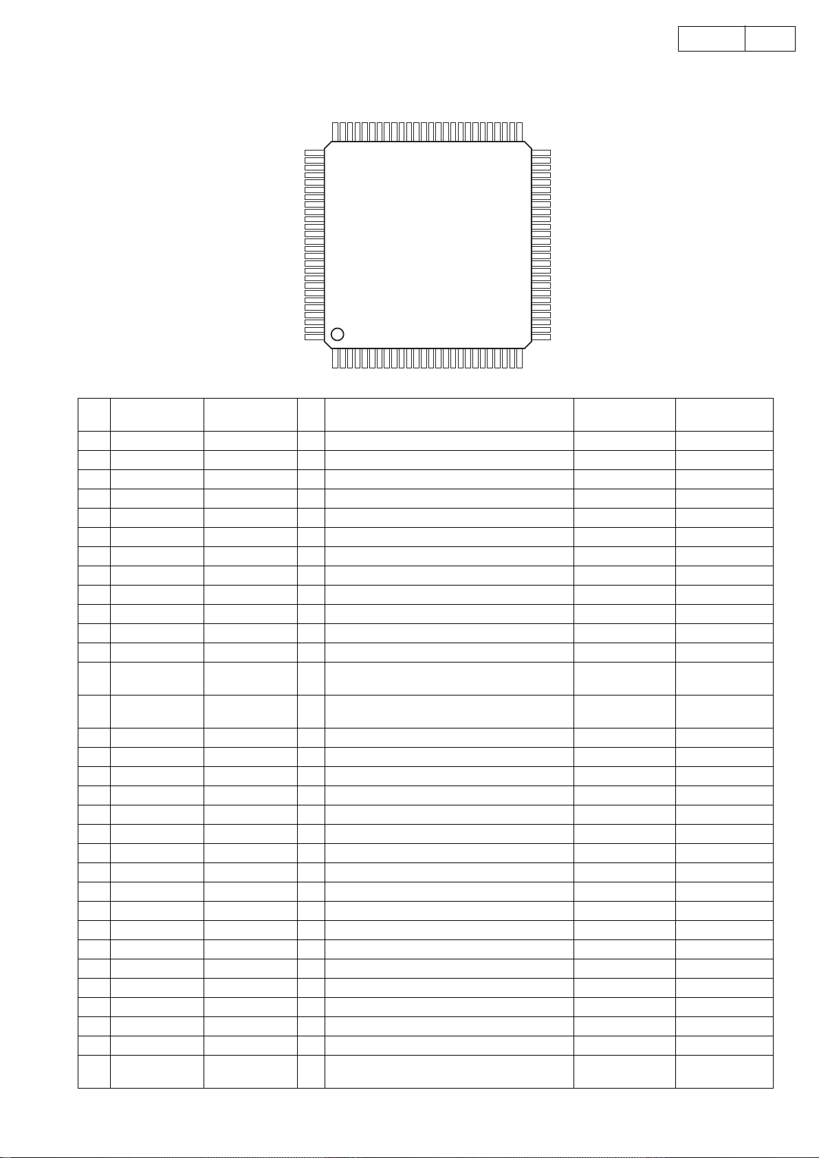
33 AVSS AVSS - A/D,D/A converter GND position OTHER -
34 P130/ANO0 LINE1 O LINE OUT Control signal output1 OTHER L
35 P131/ANO1 LINE2 O LINE OUT Control signal output2 OTHER L
36 AVref1 Avref1 - D/A converter reference voltage input OTHER -
37 P70/RxD2/SI2 SQOUT I Sub Q code data input CD L
38 P71/TxD2/SO2 COIN O CD-DSP serial communication data output CD L
39 P72/ASCK2/
SCK2
CQCK O CD-DSP serial communication clock output CD L
40 P20/RxD1/SI1 NC I Pull up RECIEVER -
41 P21/TxD1/SO1 FLDT O DATA BUS for FL driver, Data output RECIEVER L
42 P22/ACSK1/
SCK1
FLCLK O DATA BUS for FL driver, Clock output RECIEVER L
43 P23/PCL NC I Pull up RECIEVER -
44 P24/BUZ /RDSRST O RDS IC reset output RECIEVER -
45 P25/SI0/SDA0 DB RXD I DATA BUS for DENON BUS Data input RECIEVER -
46 P26/SO0 DB TXD O DATA BUS for DEON BUS Data output RECIEVER L
47 P27/SCK0/SCL0 DB CLK O DENON BUS Clock output RECIEVER L
48 P80/A0 /SD I FM/AM Tuning signal input, Tuned:Low RECIEVER -
49 P81/AÇP /ST INC I FM stereo demodulation detect input, Ste-
reo:Low
RECIEVER -
50 P82/A2 /TMUTE O Tuner mute output, mute:Low RECIEVER L
51 P83/A3 AUTO/MONO O FM AUTO/MONO switching, MONO:High RECIEVER L
52 P84/A4 USA I Initial setting input RECIEVER -
53 P85/A5 EURO I Initial setting input RECIEVER -
54 P86/A6 FREQ I Initial setting input RECIEVER -
55 P87/A7 RDS I Initial setting input RECIEVER -
56 P40/AD0 SL+ O SLIDE kick Forward CD L
57 P41/AD1 SL- O SLIDE kick Reverse CD L
58 P42/AD2 CD/!RW O CD, CD-RW gain switching CD L
59 P43/AD3 SERACH O SEARCH control CD L
60 P44/AD4 NC O OPEN CD L
61 P45/AD5 NC O OPEN CD L
62 P46/AD6 LED POWER G O POWER/STANDBY Green LED out-
put,Light:High
63 P47/AD7 LED POWER R O POWER/STANDBY Red LED output,Light:High
64 P50/A8 NC I Pull up CD -
65 P51/A9 NC I Pull up CD -
66 P52/A10 CLSW I LOADER CLOSE SW input CD -
67 P53/A11 OPSW I LOADER OPEN SW input CD -
68 P54/A12 NC I Pull up CD -
69 P55/A13 NC I Pull up CD -
70 P56/A14 NC I Pull up CD -
71 P57/A15 O Not used :NC OTHER L
72 VSS VSS - GND potential OTHER -
73 P60/A16 BLK O FLD ON/OFF control port, L= black out FLD
74 P61/A17 DATXD O DATA BUS(for VOL,PLL,RDS IC, EEPROM)
Data output
RECIEVER L
75 P62/A18 DACLK O DATA BUS(for VOL,PLL,RDS IC, EEPROM)
Clock output
RECIEVER L
76 P63/A19 DACE O DATA BUS(for VOL,PLL,RDS IC) Chip enable
output
RECIEVER L
77 P64/RD DRP_RST O CD-DSP reset output, output, reset:High CD L
78 P65/WR O Not used :NC OTHER L
79 P66/WAIT PWBCHK I Start PWB check mode OTHER -
Pin
No. Port Symbol I/O Function RECIEVER or CD outputs of
standby&Defoult

11
11UD-M31
80 P67/ASTB O Not used :NC OTHER L
81 VDD VDD - Positive power OTHER -
82 P100/TI5/TO5 OPEN O CD mecha. Open CD L
83 P101/TI6/TO6 CLOSE O CD mecha. Close CD L
84 P102/TI7/TO7 O NC OTHER L
85 P103/TI8/TO8 O NC OTHER L
86 P30/TO0 RWC O CD-DSP serial communication read / write CD L
87 P31/TO1 O Not used :NC OTHER L
88 P32/TO2 DRV_MUTE O DRIVER MUTE CD L
89 P33/TI1 O Not used :NC, CD L
90 P34/TI2 CDPOWER O CD power control signal output CD L
91 P35/TI00 O Not used :NC, OTHER L
92 P36/TI02 O Not used :NC OTHER L
93 P37 HPSW I HEADPHONE Insertswitch detective signal input
94 TEST/VPP TEST I not used :Connect to GND OTHER -
95 P90 O Not used :NC, OTHER L
96 P91 OPSW I Pickup inner-most detect input, inner most:Low
at on
-
97 P92 O Not used :NC OTHER L
98 P93 O Not used :NC OTHER L
99 P94 O Not used :NC OTHER L
100 P95 O Not used :NC OTHER L
Pin
No. Port Symbol I/O Function RECIEVER or CD outputs of
standby&Defoult

12
12UD-M31
LC78625E(IC803)
Synchronization
detection
EFM Demodulation
Slice Level
Control
CLV
Digital servo
Subcode
separation
Q CRC
Microprocessor
Interface
VCO
oscillator
Clock control
2k
´
8-bit
RAM
RAM address
generator
C1 and C2 error
detection and correction
Flag processing
General-purpose
ports/Anti-shock
interface
8
´
oversampling
digital filters
One-bit D/A
converter
Crystal oscillator system
Timing generator
DEFI
EFMIN
FSEQ
CLV+
CLV-
V/P
SFSY
CS
WRQ
SQOUT
CQCK
CO IN
RWC
FST
FOCS
FZD
TOFF
JP-
JP+
THLD
TGL
EMPH
EFLG
16M
4.2M
CK2
FSX
XV
SS
XOUT
XIN
XV
DD
RV
DD
MUTER
RCHP
RCHN
LCHN
LCHP
LV
SS
MUTEL
LRCKO
DFORO
DFOLO
DACKO
DOUT
ROMXA
C2F
LRSY
V
SS
V
DD
TEST3
TEST4
TEST5
TEST1
TEST2
TAI
PCK
FR
ISET
PDO
VV
SS
VV
DD
EFMO
TST11
PW
SBCK
SBSY
DEMO
EFMO
TST10
Level meter
Peak meter
Interpolation
and mute
Bilingual function (1)
Digital output
Bilingual function (2)
Digital
attenuator
ASDACK/P0
ASDFIN/P1
ASDEPC/P2
ASLRCK/P3
LV
DD
HFL
TES
Servo
commander
RES
LASER
CONT
RV
SS
SQOUT
CO IN
ASDEPC/P2
ASDFIN/P1
ASDACK/P0
TST10
DACKO
DFOLO
DFORO
LRCKO
12345678910 11 12 13 14 15 16 17 18 19 20 21 22 23 24
4142
43
44
45
46
47
48
49
50
5152
53
54
55
56
57
58
59
6061
626364
RWC
WRQ
FSX
SBCK
SFSY
PW
EFLG
SBSY
DOUT
MUTER
RV
DD
RCHP
RCHN
RV
SS
LV
SS
LCHN
LCHP
LV
DD
MUTEL
C2F
ROMXA
CK2
LRSY
ASLRCK/P3
EMPH
TEST4
DEMO
JP-
JP+
V
DD
TEST3
THLD
DEFI
TAI
PDO
VVSS
ISET
VVDD
FR
VSS
EFMO
EFMO
EFMIN
TEST2
CLV+
CLV-
V/P
FOCS
FST
FZD
HFL
TES
PCK
FSEQ
TOFF
TGL
CQCK
RES
TST11
LASER
16M
4.2M
CONT
TEST5
CS
XV
SS
XIN
XOUT
XV
DD
TEST1
65
66
67
68
69
70
71
72
73
74
75
76
77
78
79
80
40
39
38
37
36
35
34
33
32
31
30
29
28
27
26
25

13
13UD-M31
LC78625E Terminal Function
PinNo. Symbol I/O Function
1 DEFI I Defect detection signal (DEF) input (This pin must be connected to 0 V if unused.)
2TAII
PLL pins
Test input. A pull-down resistor is built in. (This pin must be connected to 0 V in normal
operation.)
3 PDO O External VCO control phase comparator output
4VVSS Internal VCO ground. (This pin must be connected to 0 V.) PLL pins
5 ISET AI PDO output current adjustment resistor connection
6VVDD Internal VCO power supply.
7 FR AI VCO frequency range adjustment
8 VSS Digital system ground. (This pin must be connected to 0 V.)
9EFMOO
Slice level control
EFM signal inverted output
10 EFMO O EFM signal output
11 EFMIN I EFM signal input
12 TEST2 I Test input. A pull-down resistor is built in. This pin must be connected to 0 V in normal operation.
13 CLV+O Spindle servo control output. Acceleration when CLV+ is high, deceleration when CLV- is high.
14 CLV-O Three-value output is also possible when specified by microprocessor command.
15 V/P O Rough servo/phase control automatic switching monitor output. Outputs a high level during rough servo and a low
level during phase control.
16 FOCS O Focus servo on/off output. Focus servo is on when the output is low.
17 FST O Focus start pulse output. This is an open-drain output.
18 FZD I Focus error zero cross signal input. (This pin must be connected to 0 V if unused.)
19 HFL I Track detection signal input. This is a Schmitt input.
20 TES I Tracking error signal input. This is a Schmitt input
21 PCK O EFM data playback clock monitor. Outputs 4.3218 MHz when the phase is locked.
22 FSEQ O Synchronization signal detection output. Outputs a high level when the synchronization signal detected from the
EFM signal and the internally generated synchronization signal agree.
23 TOFF O Tracking off output
24 TGL O Tracking gain switching output. Increase the gain when low.
25 THLD O Tracking hold output
26 TEST3 I Test input. A pull-down resistor is built in. (This pin must be connected to 0 V.)
27 VDD Digital system power supply.
28 JP+OTrack jump output. A high level output from JP+ indicates acceleration during an outward jump or deceleration dur-
ing an inward jump.
29 JP-OA high level output from JP- indicates acceleration during an inward jump or deceleration during an outward
jump.Three-value output is also possible when specified by microprocessor command.
30 DEMO I Sound output function input used for end product adjustment manufacturing steps. A pull-down resistor is built in.
(This pin must be connected to 0 V.)
31 TEST4 I Test input. A pull-down resistor is built in. (This pin must be connected to 0 V.)
32 EMPH O De-emphasis monitor pin. A high level indicates playback of a de-emphasis disk.
33 LRCKO O
Digital filter outputs
Word clock output
34 DFORO O Right channel data output
35 DFOLO O Left channel data output
36 DACKO O Bit clock output
37 TST10 O Test output. Leave open. (Normally outputs a low level.)
38 ASDACK
/P0 I/O When antishock
mode is not
used,these pins are
used as general pur-
pose I/O ports (P0 to
P3). They must either
be set to input mode
and connected to 0 V,
or set to output mode
and left open, if
unused.
The antishock inputs in antishock
mode.
Bit clock input
39 ASDFIN/
P1 I/O Left and right channel data input
40 ASDEPC
/P2 I/O Sets the built-in de-emphasis filter on or off.(High:
on, low: off)
41 ASLRCK/
P3 I/O L/R clock input

14
14UD-M31
Note: All power-supply pins (VDD, VVDD, LVDD, RVDD, and XVDD) must be connected to the same potential.
42 LRSY O
ROMXA application
output signals
L/R clock output
43 CK2 O Bit clock output(after reset) Inverted polarity clock output(during CK2CON
mode)
44 ROMXA O Interpolation data output(after reset) ROM data output (during ROMXA mode)
45 C2F O C2 flag output
46 MUTEL O
One-bit D/A converter
signals
Left channel mute output
47 LVDD Left channel power supply
48 LCHP O Left channel P output
49 LCHN O Left channel N output
50 LVSS Left channel ground. Must be connected to 0 V.
51 RVSS Right channel ground. Must be connected to 0 V.
52 RCHN O Right channel N output
53 RCHP O Right channel P output
54 RVDD Right channel power supply
55 MUTER O Right channel mute output
56 DOUT O Digital output
57 SBSY O Subcode block synchronization signal output
58 EFLG O C1, C2, single and double error correction monitor pin
59 PW O Subcode P, Q, R, S, T, U and W output
60 SFSY O Subcode frame synchronization signal output. This signal falls when the subcodes are in the standby state.
61 SBCK I Subcode readout clock input. This is a Schmitt input. (This pin must be connected to 0 V if unused.)
62 FSX O Output for the 7.35 kHz synchronization signal divided from the crystal oscillator
63 WRQ O Subcode Q output standby output
64 RWC I Read/write control input. This is a Schmitt input.
65 SQOUT O Subcode Q output
66 COIN I Command input from the control microprocessor
67 CQCK I Input for the command input acquisition clock or the SQOUT pin subcode readout clock input. This is a Schmitt
input.
68 RES I Reset input. This pin must be set low briefly after power is first applied.
69 TST11 O Test output. Leave open. (Normally outputs a low level.)
70 LASER O Laser on/off output. Controlled by serial data commands from the control microprocessor.
71 16M O 16.9344 MHz output
72 4.2M O 4.2336 MHz output
73 CONT O Supplementary control output. Controlled by serial data commands from the control microprocessor.
74 TEST5 I Test input. A pull-down resistor is built in. (This pin must be connected to 0 V.)
75 CS I Chip select input. A pull-down resistor is built in. This pin must be connected to 0 V if unused.
76 XVSS Crystal oscillator ground. Must be connected to 0 V.
77 XIN I Connections for a 16.9344 MHz crystal oscillator
78 XOUT O
79 XVDD Crystal oscillator power supply
80 TEST1 I Test input. A pull-down resistor is built in. (This pin must be connected to 0 V.)
PinNo. Symbol I/O Function

15
15UD-M31
LC75725E(IC401)
Terminal Function
Pin No. I/O Name Function
1,13 Power supply pin to driver block
2~12 Digit output pin
14~56 Segment output pin
57 power supply pin
63
64
CE : Chip enable
CL : Sync clock
DI : Transfer data
1 2 3 4 5 6 7 8 9 10111213141516
48 47 46 45 44 43 42 41 40 39 38 37 36 35 34 33
64
63
62
61
60
59
58
57
56
55
54
53
52
51
50
49
17
18
19
20
21
22
23
24
25
26
27
28
29
30
31
32 S25
S26
S27
S28
S29
S30
S31
S32
S33
S34
S35
S36
S37
S38
S40
S41
S42
S43
VFL
G11
G10
G9
G8
G7
G6
G5
G4
G3
G2
G1
VFL
S24
S23
S22
S21
S20
S19
S18
S17
S16
S15
S14
S13
S12
S11
S10
S9
S39
S8
S7
S6
S5
S4
S3
S2
S1
Vss
OSC0
OSC1
V
DD
BLK
CE
CL
DI
DIGIT
DRIVER
SEGMENT DRIVER
MPX
LATCH
DIMMER
TIMING
GENERATOR
GRID
CONTROL
SHIFT REGISTER
ADDRESS
DETECTOR
TIMING
GENERATOR
DIVIDER
CLOCK
GENERATOR
V
DD
VSS
CE
CL
DI
OSCI
OSCO
VFL
BLK
G11
G10
G2
G1
S43
S42
S2
S1
-
O
O
-
O
I
-
I
I
I
I
58 OSCO Pin for oscillator
59 OSCI Pin for oscillator
60 VDD Power supply pin to ligic block
61 BLK Display off input pin
62 CE Input for serial data transfer
VFL
G1~G11
S1~S43
Vss
CL
DI

16
16UD-M31
LA9241M(IC802)
LA9241M Terminal Function
PinNo. Symbol Contents
1FIN2
Pickup photodiode connection pin. Added to FIN1 pin to generate the RF signal, subtracted from FIN1 pin to generate
the FE signal.
2 FIN1 Pickup photodiode connection pin.
3 E Pickup photodiode connection pin. Subtracted from F pin to generate the TE signal.
4 F Pickup photodiode connection pin.
5 TB TE signal DC component input pin.
6TE-Pin which connects the TE signal gain setting resistor between this pin and TE pin.
7 TE TE signal output pin.
8 TESI TES (Track Error Sense) comparator input pin. The TE signal is input through a bandpass filter.
9 SCI Shock detection input pin.
10 TH Tracking gain time constant setting pin.
11 TA TA amplifier output pin.
12 TD-Pin for configuring the tracking phase compensation constant between the TD and VR pins.
13 TD Tracking phase compensation setting pin.
14 JP Tracking jump signal (kick pulse) amplitude setting pin.
15 TO Tracking control signal output pin.
16 FD Focusing control signal output pin.
17 FD-Pin for configuring the focusing phase compensation constant between the FD and FA pins.
18 FA Pin for configuring the focusing phase compensation constant between the FD- and FA- pins.
19 FA-Pin for configuring the focusing phase compensation constant between the FA and FE pins.
20 FE FE signal output pin.
21 FE-Pin which connects the FE signal gain setting resistor between this pin and FE pin.
22 AGND Analog signal GND.
23 NC No connection
24 SP CV+ and CV- pins input signal single-end output.
25 SPG 12-cm spindle mode gain setting resistor connection pin.
26 SP-Spindle phase compensation constant connection pin, along with the SPD pin.
27 SPD Spindle control signal output pin.
28 SLEQ Sled phase compensation constant connection pin.
29 SLD Sled control signal output pin.
30 SL-Input pin for sled movement signal from microprocessor.
31 SL+Input pin for sled movement signal from microprocessor.
NC
TBC
FSC
DGND
SLI
SLC
RFS
RFSM
CV
CV
SLOF
HFL
TES
TOFF
TGL
JP
FD
FA
FA
FE
FE
AGND
NC
SP
SPG
SP
SPD
SLEQ
SLD
SL
SL
JP
FIN2
FIN1
E
F
TB
TE
TE
SCI
TH
TA
TD
TD
JP
TESI
TO
FD
64
63
62
61
60
59
58
57
56
55
54
53
52
51
50
49
48
47
46
45
44
43
42
41
40
39
38
37
36
35
34
33
17
18
19
20
21
22
23
24
25
26
27
28
29
30
31
32
1
2
3
4
5
6
7
8
9
10
11
12
13
14
15
16
VCC1
LDS
LDD
BH1
PH1
LF2
VR
REFI
VCC2
FSS
DRF
CE
DAT
CL
CLK
DEF
-
-
+
-
-
-
-
-
-
+
-
+
-
1
2
3
4
5
6
7
8
9
10
11
12
13
14
15
16
17 18 19 20 21 22 23 24 25 26 27 28 29 30 31 32
33
34
35
36
37
38
39
40
41
42
43
44
45
46
47
48
49505152535455565758596061626364
APC
RF DET
REF
I/V VCA
VCABAL -com
INTER FACE
T. SERVO & T.LOGIC
F.SERVO & F.LOGIC SPINDLE
SERVO
SLED SERVO
TE
SLC
RF Amp
FIN2
FIN1
E
F
TB
TE
TE
SCI
TH
TA
TD
TD
JP
TESI
TO
FD
-
-
FD
FA
FA
FE
FE
AGND
NC
SP
SPG
SP
SPD
SLEQ
SLD
SL
SL
JP
+
-
-
-
-
-
-
NC
TBC
FSC
DGND
SLI
SLC
RFS
RFSM
CV
CV
SLOF
HFL
TES
TOFF
TGL
JP+
-
+
-
VCC1
LDS
LDD
BH1
PH1
LF2
VR
REFI
VCC2
FSS
DRF
CE
DAT
CL
CLK
DEF

17
17UD-M31
32 JP-Input pin for tracking jump signal from DSP.
33 JP+Input pin for tracking jump signal from DSP.
34 TGL Input pin for tracking gain control signal from DSP. Gain is low when TGL is high.
35 TOFF Input pin for tracking off control signal from DSP. Tracking servo is off when TOFF is high.
36 TES Output pin for TES signal to DSP.
37 HFL The High Frequency Level is used to determine whether the main beam is positioned over a bit or over the mirrored
38 SLOF Sled servo off control input pin
39 CV-Input pin for CLV error signal from DSP.
40 CV+Input pin for CLV error signal from DSP.
41 RFSM RF output pin.
42 RFS-RF gain setting and EFM signal 3T compensation constant setting pin, along with the RFSM pin.
43 SLC Slice Level Control is an output pin that controls the data slice level used by the DSP for the RF waveform.
44 SLI Input pin used by DSP for controlling the data slice level.
45 DGND Digital system GND pin.
46 FSC Focus search smoothing capacitor output pin.
47 TBC Tracking Balance Control; EF balance adjustment variable range setting pin
48 NC No connection
49 DEF Disc defect detection output pin.
50 CLK Reference clock input pin. 4.23 MHz signal from the DSP is input.
51 CL Microprocessor command clock input pin.
52 DAT Microprocessor command data input pin.
53 CE Microprocessor command chip enable input pin.
54 DRF RF level detection output (Detect RF).
55 FSS Focus Search Select; focus search mode (Å} search/+search vs. the reference voltage) switching pin
56 VCC2Servo system and digital system VCC pin.
57 REFI By-pass capacitor connection pin for reference voltage.
58 VR Reference voltage output pin.
59 LF2 Disc defect detection time constant setting pin.
60 PH1 RF signal peak hold capacitor connection pin.
61 BH1 RF signal bottom hold capacitor connection pin.
62 LDD APC circuit output pin.
63 LDS APC circuit input pin.
64 VCC1RF system VCC pin.
PinNo. Symbol Contents

18
18UD-M31
LA6559(IC801)
1 REV 5CH output change terminal, logic input of
loading block
2 S-Vcc signal system power supply
(BTL-AMP:CH1~4)
3 Vcc2 Power supply for loading block
4 VLO- Loading output (-)
5 VL0+ Loading output (+)
6 VO4+ Output terminal (+) for channel 4
7 VO4- Output terminal ( ) for channel 4
8 VO3+ Output terminal (+) for channel 3
9 VO3- Output terminal (- ) for channel 3
10 VO2+ Output terminal (+) for channel 2
11 VO2- Output terminal (- ) for channel 2
12 VO1+ Output terminal (+) for channel 1
13 VO1- Output terminal (- ) for channel 1
14 Vcc1 CH1 `CH4(BTL-AMP) output stage power supply
15 VIN1 Input terminal for channel 1
16 VIN1- OP-AMP input AMP-A input terminal (- )
17 VIN1+ OP-AMP input AMP-A input terminal (+)
18 VIN2 Input terminal for channel 2, input AMP output
19 VIN2- Input terminal (- ) for channel 2
20 VIN2+ Input terminal (+) for channel 2
21 Vcc-VREG 3.3VREG power supply
22 GND-VREG 3.3VREG GND
23 VIN3 Input terminal for channel 3, input AMP output
24 VIN3- Input terminal (- ) for channel 3
25 VIN3+ Input terminal (+) for channel 3
26 REG-IN PNP transistor base connected
27 REG-OUT 3.3V power output to which the PNP transistor
collector connected
28 VCONT Loading output voltage set terminal
29 VREF-IN Reference voltage applied terminal
30 VIN4+ Input terminal (+) for channel 4
31 VIN4- Input terminal (- ) for channel 4
32 VIN4 Input terminal for channel 4, input AMP output
33 MUTE1 Output ON/OFF for channel 1 (BTL AMP)
34 MUTE2 Output ON/OFF for channel 2 to 4 (BTL AMP)
35 S-GND Signal system GND
36 FWD Output change terminal (FWD) for loading
output (VLO+,-), logic input of loading block
Pin
No. Name Function
1
2
3
4
5
6
7
8
9
FR
10
11
12
13
14
15
16
17
18
36
35
34
33
32
31
30
29
28
FR
27
26
25
24
23
22
21
20
19
FWD
S-GND
MUTE2
MUTE1
VIN4
VIN4-
VIN4+
VREF-IN
VCONT(LOADING)
FR
REG-OUT
REG-IN
VIN3+
VIN3-
VIN3
GND-VREG
VCC-VREG
VIN2+
VIN2-
REV
S-VCC
VCC2
VLO-
VLO+
VO4+
VO4-
VO3+
VO3-
FR
VO2+
VO2-
VO1+
VO1-
VCC1
VIN1
VIN1-
VIN1+
VIN2
Signal System VCC
(CH1 to CH4)
33k
11k
33k
11k
3.3VREG GND
3.3VREG
33k
11k
3.3VREG PNP Tr
Base
PNP Tr
Collector
33k
11k
CH1 Output
ON/OFF
CH2 to CH4
Output
MUTE1
MUTE2
(LOADING)
Power Supply Input
(Forward/Reverse/
Break/OFF)
Output
Control
Level
Shift
Level
Shift
Power
System
GND
Level
Shift
Level
Shift
Power Supply
Power Supply
(External PNP)
Power System GND
Signal System GND
Thermal
Shutdown
-
)
S
11k
PNP Tr
Base
11k
t
(LOADING)
Power Supply Input
(For rd/Reverse/
Output
Power
System
ft
u
)
T
Sh

19
19UD-M31
LC75342M(IC302)
LC72720NM(IC303)
+
-
+
-
+
-
+
-
-
+
-
+
-
-
++
+
-
+
-
CONTROL
CIRCUIT
LOGIC
CIRCUIT
CONTROL
CIRCUIT
1
2
3
4
5
6
7
8
9
10
11
12
13
14
15
30
29
28
27
26
25
24
23
22
21
20
19
18
17
16
DI
CE
VSS
TEST
LOUT
LBASS2
LBASS1
LTRE
LIN
LSELO
L4
L3
L2
L1
NC
CL
VDD
VREF
NC
ROUT
RBASS2
RBASS1
RTRE
RIN
RSELO
R4
R3
R2
R1
NC
ROUT RBASS2 RBASS1 RTRE RIN RSELO
212223242526
27
28
29
30
1
2
3
4
567 8910
LSELO
L4
L3
L2
L1
NC
NC
R1
R2
R3
R420
19
18
17
16
15
14
13
12
11
LIN
LTRELOUT
TEST
Vss
CE
DI
CL
VDD
Vref
NC
LBASS1
LBASS2
RVref
LVref
CCB
INTERFACE
24
23
22
21
20
19
18
17
16
15
14
13
1
2
3
4
5
6
7
8
9
10
11
12
Vref
MPXIN
Vdda
Vssa
FLOUT
CIN
T1
T2
T3 (RDCL)
T4 (RDDA)
T5 (RSFT)
XOUT
SYR
CE
DI
CL
DO
RDS-ID
SYNC
T7 (CORREC/ARI-ID/BEO)
T6 (ERROR/57K/BE1)
Vssd
Vddd
XIN
REFERENCE
VOLTAGE
ANTIALIASING
FILTER
57kHz
BPF
(SCF) SMOOTHING
FILTER
PLL
(57kHz)
CLOCK
RECOVERY
(1167.5Hz)
RAM
(24 BLOCK DATA)
ERROR CORRECTION
(SOFT DECISION)
DATA
DECODER
SYNC/EC CONTROLLER
CCB
TEST
VREF
VREF
MEMORY CONTROL
OSC/DIVIDER
SYNC
DETECT-1
SYNC
DETECT-2
CLK(4.332MHz)
FLOUT CIN
Vdda
Vssa
MPXIN
DO
CL
DI
CE
T1
T2
T3 T7
XIN XOUT
Vddd
Vssd
RDS-ID
SYNC
SYR

20
20UD-M31
STK402-050(IC501)
BA6287F(IC805)
93LC66(IC202)
M51957BFP(IC205)
9
4
1
2
SUB
13 512 7610 11 14 15
8
TR3
R2
TR7
R6
C1 C2
TR11
TR9
R14
TR16
TR14 TR15
R13
TR4
TR1 TR2 R3
R4
R5
D1
TR6
R7
R8
R11
R12
TR12
TR10
R10
TR13
R9
TR5
TR8
R1
115
FRONT VIEW
1
2
3
45
6
7
8
CS
SK
Vcc
DI
DO
WP
ORG
GND
INSTRUCTION
REGISTER
INSTRUCTION
DECODE
CONTROL
AND
CLOCK
GENERATION
DATA
REGISTER
ADDRESS
REGISTER
Vcc RANGE
DETECTOR
WRITE ENABLE
DUMMY BIT
R/W AMPS
HIGH VOLTAGE
GENERATOR
DECODER MEMORY ARRAY
256/512 X 8
OR
64/128/256 X 16
DI
CS
SK
(2K/4K)
ORG
DO
1
2
3
4
5
7
8
6
NC
NC
NC
GND
TOP VIEW
IN V
CC
OUT
Delay Cap.
Other manuals for UD-M31
3
Table of contents
Other Denon Car Receiver manuals

Denon
Denon UD-M31 User manual

Denon
Denon tu-245 User manual

Denon
Denon CEOL RCD-N8 User manual

Denon
Denon CEOL RCD-N12 User manual

Denon
Denon CEOL RCD-N8 User manual

Denon
Denon RCD-M33 User manual

Denon
Denon RCD-M39 User manual

Denon
Denon RCD-M39 User manual

Denon
Denon CEOL RCD-N12 User manual

Denon
Denon RCD-M40 User manual
Popular Car Receiver manuals by other brands

Jensen
Jensen Phase Linear SD1413 owner's manual

AEG
AEG AR 4030 BT/USB/CR instruction manual

Blaupunkt
Blaupunkt Montreux RCM 45 operating instructions

Blaupunkt
Blaupunkt HAMBURG MP57 Operating and installation instructions

Kenwood
Kenwood KDC-X492 - eXcelon Radio / CD instruction manual

Jensen
Jensen Receiver CD2610 quick start guide