1.3.1
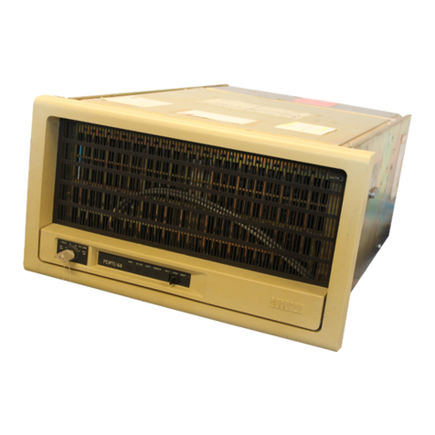
PDP-ll/40
Computer
The
PDP-ll/40
is
a 16-bit general purpose, parallel logic,
microprogrammed
computer
using single
and
double oper-
and
instructions and
2's
complement
arithmetic.
The
PDP-l1/40
contains a multiple
word
instruction processor,
which can directly address
up
to
28K
words
of
core
memory.
All
communication
among system
components
(including processor, core memory, and peripherals)
is
performed
on
a single high-speed bus,
the
Unibus. Because
of
the
bus concept,
all
peripherals are compatible, and
device-to-device transfers can be accomplished
at
the
rate
of
2.5
million words per second. All system
components
and
peripherals are linked
by
the
Unibus and power connectors,
and
all peripherals are in
the
basic system address space.
Therefore,
all
instructions applied
to
data
in
memory
can
also be applied
to
data
in
peripheral device registers,
enabling peripheral device registers
to
be manipulated
by
the
processor as flexibly as memory.
Subsequent
paragraphs present a brief functional descrip-
tion
of
the
PDP-ll/40.
1.3.1.1 Unibus -
The
Unibus provides high-speed com-
munication between system
components.
With bidirectional
data,
address,
and
control lines,
the
Unibus allows
data
transfers
to
occur between all units
on
the
bus, with control
of
the
bus an
important
factor
in
these transfers.
The
fixed
repertoire
of
bus operations
is
flexible enough for speed
and
design
economy,
yet
provides a fixed specification for
interfaces. The asynchronous nature
of
these operations
also eases design
and
operation.
The
repertoire
of
bus
operations
is: ,
DATI, DATIP, DATO, DATOB -data operations
INTR, PTR (BR, NPR) -control operations
Full 16-bit words
or
8-bit bytes
of
information can be
transferred
on
the
bus between
the
master
and
slave.
The
DATI, DATIP operations transfer data into
the
master;
DATO, DATOB operations transfer
data
out
of
the
master.
When a device
is
capable
of
becoming bus master and
requests use
of
the
bus, it
is
for
one
of
two
purposes:
to
make a Direct Memory Access (DMA) transfer of data
directly
to
or
from
another
device
or
memory
without
processor intervention,
or
to
INTeRrupt
(lNTR) program
execution
and force
the
processor
to
branch
to
a specific
address where an
interrupt
service
routine
is
located.
Bus
control
is
obtained
under a Non-Processor Request
(NPR)
for
the
DMA
or
under a Bus Request (BR) for an
INTR. A device can perform a
DMA
after
acquiring bus
control
via
a BR.
2
Requests for
the
bus can be made
at
any
time
on
the
BR
and
NPR lines. Transfer
of
bus control from
one
device
to
another
is
made by
the
processor priority arbitration logic
which grants control
of
the
bus
to
the
device having
the
highest priority. NPRs are accorded higher priority
than
BRs.
The
NPRs are serviced before
and
immediately
after
Unibus data cycles, in
addition
to
specific times during
WAIT
or
TRAP
sequences.
The
BRs are serviced upon
completion
of
the
current
instruction
if
the
requesting
priority exceeds
that
of
the
processor.
The
PDP-l1
/40
processor has a special role
in
bus control
operations
as
it performs
the
priority arbitration
to
select
the
next
bus master.
The
processor assumes bus control
when no
other
device has
control.
The
Unibus originates
in
the
processor with
the
M981
Internal Unibus
and
Terminator
module, which carries
the
Unibus
from
the
processor
to
the
next
system unit.
All
56
Unibus signals
and
17
grounds are carried
in
this
one
module. A
120-conductor
Mylar cable
is
used
to
connect
system units
in
different mounting boxes
or
to
connect
a
peripheral device removed
from
the
mounting box.
A
complete
description
of
the
Unibus, including specifica-
tions,
is
presented in
the
PDP-11 Peripherals Handbook.
1.3.1.2
KDll-A
Processor-The
KD11-A Processor de-
codes instructions; accepts, modifies, and
outputs
data;
performs
arithmetic
operations; and controls allocation
of
the
Unibus among external devices.
The
processor contains
sixteen hardware registers, eight
of
which are program-
mable.
Two
of
the
eight programmable registers are
specifically used for processor operation: a program count-
er (PC)
and
a stack
pointer
(SP);
the
remaining six serve as
arithmetic
accumulators, index register, and
autoincrement
and
autodecrement
registers.
The
eight non-programmable registers are used for storage
of a variety
of
functions including: intermediate address,
source
and
destination
data, a copy of
the
instruction
register,
the
last
interrupt
vector address and console
operation
data.
Because
of
the
flexibility
of
hardware registers, address
modes, instruction set,
and
DMA, PDP-11
/40
programs are
written
in directly relocatable codes.
The
processor also
includes a full
complement
of
instructions
that
manipulate
byte
operands and provisions for
byte
swapping. Either
words or bytes may be displayed on
the
programmer's
console.
