The bipolar and
MOS
semiconductor memories can be jointly or separately operated from either the
KB
11
Fastbus or the PDP-II Unibus, or from both, depending on the specific PDP-l 1/45 System configuration. When
operated from the Unibus, each semiconductor memory system functions
as
a PDP-II compatible peripheral
and can serve
as
the basic memory in a large-scale system. Operation underjoint control
of
the Fastbus and
Unibus provides direct high-speed memory access through the Fastbus for the
KB
11
Processor, while maintain-
ing the processor/peripheral relationships characteristic
of
the Unibus. Whether operating jointly or separately
with the Unibus and/or Fastbus, a semiconductor memory always assumes the role
of
a "slave" device
to
the
processor. Under Unibus control, the memory also
is
"slave" to any peripheral (direct access) device currently
designated "master".
Because readout from semiconductor memories
is
non-destructive, the write-after-read-cycle time associated with
ferrite-core memories
is
eliminated. In addition, the switching speed for semiconductor memories
is
characteris-
tically much faster than
that
for
the
ferrite-core memory. The extremely high switching speeds characteristic
of
bipolar memory
cells
permit memory cycle times
of
300
ns
for an operating bipolar memory system.
MOS
semiconductor memory systems have slower cycle times
of
450 ns.
1.2
M8111 BIPOLAR MEMORY
MATRIX
MODULE
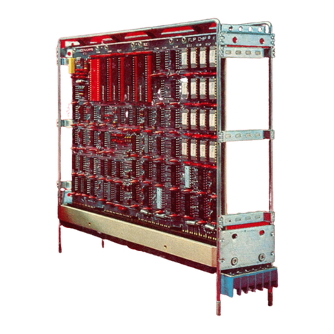
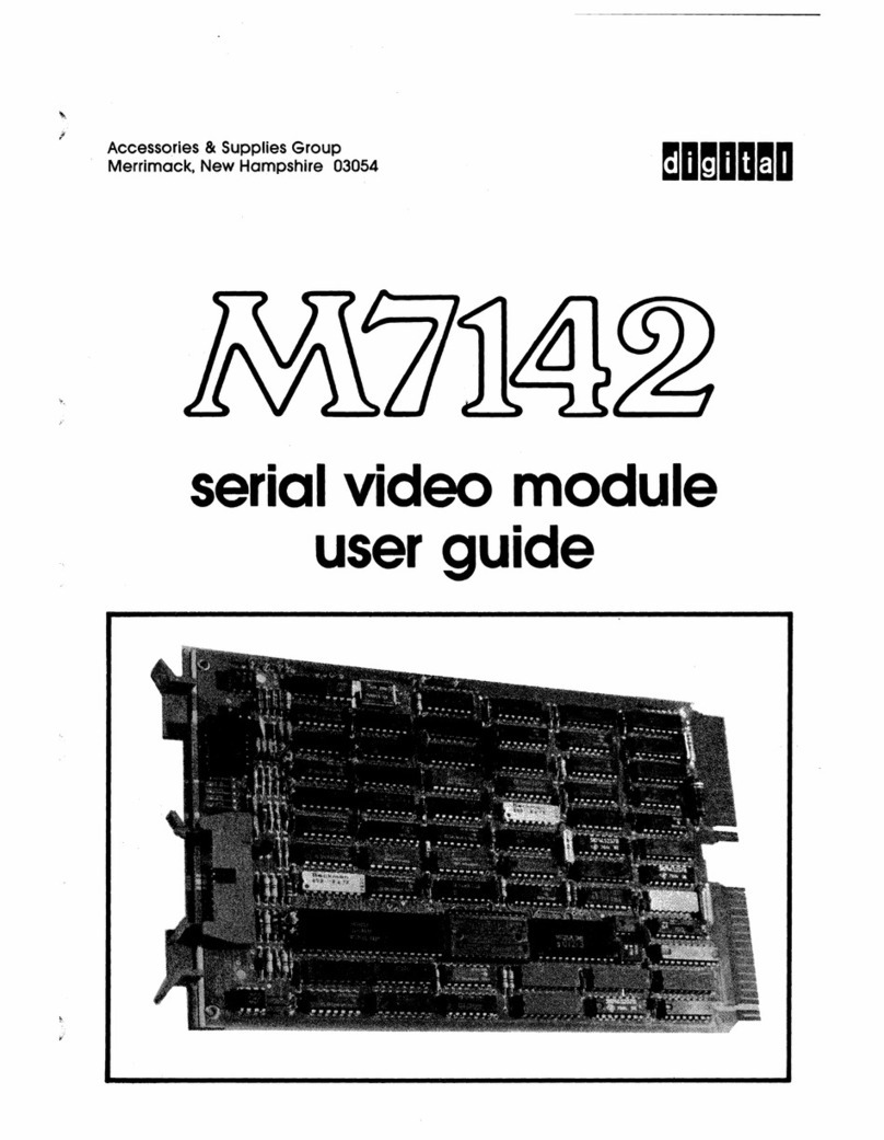
The M8111 Bipolar Memory Matrix module
is
an 8-1/2 in
..
X
15
in. multilayer glass hex board, configured to
either store or not store byte parity. The M811I
YA
parity-equipped modules contain seventy-two 256 X I-bit
TTL
MSI
memory circuits, interconnected to form a 1024 X IS-bit memory matrix. Each IS-bit word in this
matrix
is
formed by two S-bit bytes and two parity bits, one per byte. This module also contains appropriate
address decoding and driving logic, IS write-data inversion stages, and control-signal decoding logic. All decod-
ing inversion and driving logic
is
formed by TTL integrated circuits. Address lines
<14:
II>
at each
MSlll
matrix
module are jumper-connected so
that
in a given bipolar memory system each matrix module can be configured
to decode a unique address. The MS111 Bipolar Memory Matrix module
is
identical to the M8111YA in all
respects, except that the MSl11 contains sixty-four 256 X I-bit
MSI
memory circuits, interconnected to form
a 1024 X 16-bit memory matrix without byte parity.
1.3 G401
MOS
MEMORY
MATRIX
MODULE
The G401
MOS
Memory Matrix module
is
an S-1/2 in. X
15
in. double-sided, multilayer
glass
hex circuit board;
also configured to either store or
not
store byte parity. The G401YA parity-equipped module contains seventy-
two 1024 X I-bit
MOS
MSI
circuits, interconnected to form a 4096 X IS-bit memory. The IS-bit word configu-
ration
is
exactly the same
as
the bipolar matrix, i.e., two S-bit bytes and two parity bits, one per byte. This mod-
ule also contains appropriate logic to level-shift addresses, data, and control signals from TTL to
MOS
and
MOS
to TTL voltage levels; and 16 or IS intergrated-circuit sense amplifiers, depending on whether parity
is
specified,
one for each
of
the read-sense lines. The states
of
memory address (MAD) register bits (02:01) and
<14:
13) are
decoded at this module to select the specific module and the group
of
1024 words addressed within the selected
module. Addtess bits
MAD
<I
4:
13)
are jumper-connected
so
that
each 4096-word matrix can be selected and
wired for a unique address assignment. The G401
MOS
Memory Matrix module
is
identical in all respects to the
G40lY
A,
except that the G401 contains sixty-four 1024 X I-bit
MSI
memory circuits, interconnected
to
form
a 4096 X 16-bit memory matrix without byte parity.
Operation
of
the
MOS
memory matrix
is
substantially different from
the
bipolar matrix in two respects. First,
because
of
the nature
of
the dynamicMOS storage cell (Appendix A), each memory access must include a time
interval for precharging the addressed cells prior
to
the actual access. Second, all memory locations in an
MOS
system must be periodically refreshed, usually every 1
ms,
to assure data validity during any extended standby
intervals.
1-2