HOLT HI?1590 User manual

AN-1590 Rev. B Holt Integrated Circuits
HI-1590 1553B Dual Transceiver
with SPI Amplitude Control
Evaluation Board
April 2018

AN-1590
2 Holt Integrated Circuits
REVISION HISTORY
Revision
Date
Description of Change
AN-1590 Rev. New
10-10-14
Initial Release
Rev. A
03-14-17
Reformat document to newer template.
Update schematic to correct error in wiring of J1, Bus B
connector.
Remove obsolete section on Freescale Development
Tools. New Instructions included separately with Kit.
Rev. B
04-09-18
Update schematic and BOM to include TVS hot switching
protection diodes.

AN-1590
3 Holt Integrated Circuits
INTRODUCTION
The Holt HI-1590 Evaluation Board demonstrates features of the HI-1590 MIL-STD-1553B dual
transceiver IC. This device transmits and receives Manchester encoded 20 bit MIL-STD-1553B
serial data suitable bus transformers. Transceiver drive amplitude can be digitally adjusted from
0 to 26 Vp-p through the SPI interface. Adjustment can also be made with a 0 to 3.3VDC analog
control signal; a potentiometer is provided for this. Amplitude controls for both buses are
ganged together. In SPI mode, a low range option allows for more accurate amplitude
adjustment from 0 to 4.9 Vp-p. The board runs from a single 3.3V ±5% supply voltage. A MIL-
STD-1553B protocol message generator and receiver are included on the board to demonstrate
the HI-1590 features. The EVM (Evaluation Module) includes a microcontroller that generates
the SPI messages, the interface is through a terminal emulator connected to a PC through the
USB interface. The EVM is shown in the picture below:
Fig 1 –HI-1590 Evaluation Board

AN-1590
4 Holt Integrated Circuits
This guide summarizes how to set up and running quickly.
KIT CONTENTS
This User Guide
HI-1590 Evaluation Board
Mini USB Serial Cable.
Board Block Diagram
MC9S12XD
16 Bit MCU
SPI
USB
DIP SW
(4) DIP SW(6)
RESET Button
3.3V
Supply
RESET Transceiver A DB2791
TRANSFORMER
HI-1590
BUSA
Transceiver B DB2791
TRANSFORMER BUSB
Message A
1553B
Message
Generator
Message B
RUN
EEPROM
1EEPROM
2
BC RT DIP SW
(5)
DIP SW
(5)
ANALOG CONTROL
VCONT
ACTIVE

AN-1590
5 Holt Integrated Circuits
LED Functions
REF
NAME
DEFAULT
DESCRIPTION
LED1
POWER
ON
Indicated when 3.3V power is present
LED2
ACTIVE
OFF
Flashes at the start of a 1553 message transmit sequence
Link Jumper Functions
REF
NAME
DEFAULT
DESCRIPTION
J4
LINK FOR POT
OFF
Link to use potentiometer R3 to adjust output amplitude
J5
LINK FOR SPI
ON
Link to use SPI to adjust output amplitude
J8
HOLD IN RESET
OFF
Holds the microcontroller in reset, for instance while using
an external SPI interface.
J12
BC/RT
BC
Connects memory for BC or RT messages
Wired Jumper Functions (JP)
REF
NAME
DEFAULT
DESCRIPTION
JP1
ON
Link to use on-board 70 Ωload on Bus B output
JP8
ON
Link to use on-board 70 Ωload on Bus A output
JP2, 3, 4, 5
JP4, 5 ON
Option links for transformer variants, Bus B
JP6, 7, 9, 10
JP6, 9 ON
Option links for transformer variants, Bus A
JP11
ON
Connects Bus A negative output to ground
JP12
ON
Connects Bus B negative output to ground
JP13-16
ON
Cut if using an external 1553 message generator

AN-1590
6 Holt Integrated Circuits
Switch Functions
REF
NAME
DEFAULT
DESCRIPTION
SW1/1
VSEL
ON
Selects output control of amplitude range, using SPI.
ON = SPI control 0-24V, Low = SPI, 0-2.4V
SW1/2
TXAINH
OFF
Inhibits the transmitter output of transceiver A
SW1/3
TXBINH
OFF
Inhibits the transmitter output of transceiver B
SW1/4
RXAEN
ON
Enables the receiver of transceiver A
SW1/5
RXBEN
ON
Enables the receiver of transceiver B
SW3
RUN
Press = Starts 1553 messages
SW4
STOP
Press = Stops 1553 messages
SW5/1-5
AUTOEN etc
01101
Message loading control (leave in default)
SW6/1-6
RT1A4:0, RT1AP
000000
RT Address (only used if RT mode available)
SW7
RESET
Press to reset the microcontroller and control software
Connector Functions
REF
NAME
DESCRIPTION
J1
BUSB
1553 Bus A connection (secondary of transformer)
J2
BUSA
1553 Bus B connection (secondary of transformer)
J3/ 1,2
RXA/nRXA
Differential Logic signal from HI-1590 Bus A receive data pins
J3/ 3,4
RXB/nRXB
Differential Logic signal from HI-1590 Bus B receive data pins
J6
Not fitted
SPI interface for the EEPROMs
J7
Data connector to load 1553 messages
J9
USB
Connect to PC to send SPI commands from terminal emulator
J10
External SPI
Use to connect an external SPI for HI-1590 control
J11
Debug Header
Used for downloading microcontroller firmware

AN-1590
7 Holt Integrated Circuits
Test Point Functions
REF
NAME
DESCRIPTION
TP1/TP2
BUSB
1553 Bus B connection (secondary of transformer)
TP4/TP6
BUSA
1553 Bus A connection (secondary of transformer)
TP3, 8,9,10
GND
Board Ground
TP5
VCONT
Connection to measure of input analog amplitude control, note that
J5 should be open. J4 should be open when inputting a voltage.
TP6
UPDATE
Test point for Update signal indicates when MIL-STD-1553B word has
been received
TP7
VSEL
This pin monitors voltage on the VSEL pin control on the output
amplitude.
High = SPI control 0-24V
Float = Analog Control
Low = SPI Control, 0-5.1V
TP3, 8, 9, 10
GND
Board Ground
TP11
3V3
VLOGIC Supply, connect power supply here
TP21
VDD
VLOGIC after supply filter
TP13
IRQ
INTERRUPT
TP14
ACTIVE
Produces pulse just before 1553 message starts, can be used to
trigger scope.
TP17/18
TXDO/RXDO
USB data.
TXA, nTXA
Connect external 1553 data here if not using the on board message
generator for BUSA. Need to cut links TXA and nTXA.
TXB, nTXB
Connect external 1553 data here if not using the on board message
generator for BUSB. Need to cut links TXB and nTXB.

AN-1590
8 Holt Integrated Circuits
Using the Board
1. Check all the link and switch positions comply with the tables above. Connect a 3.3V, 1A
supply to the 3V3 test point. A 1A supply current is required at maximum amplitude. Verify
the ‘Power On’ LED is lit; the board should take about 160mA, when not sending 1553
messages. Connect the mini USB lead to your PC and then to the HI-1590 board. Your PC
should automatically install the driver, if not the driver FT231 can be installed from the Holt
CD. If you have problems installing the driver please refer to the FTDI website below:
http://www.ftdichip.com/Documents/InstallGuides.htm
2. All control of the HI-1590 is done through the ‘Control Console’. This requires use of a
terminal emulator for communication, such as HyperTerminal or Tera Term. Tera Term is
used with Windows versions of Vista or later and is supplied on the Holt CD.
To install Tera Term:
Use the Tera Term installer program teraterm.exe from the Holt CD. Accept the license
agreement stating redistribution is permitted provided that copyright notice is retained.
The notice can be displayed from the Tera Term window by clicking Help then clicking
About Tera Term. Continuing to install…
Accept the default install destination and click Next.
At the Select Components screen, unselect all options except Additional Plugin =
TTXResizeMenu and click Next.
Select the installed language, then click Next.
Accept the default Start Menu folder, then click Next.
Select any desired shortcuts, then click Next.
At the Ready to Install screen, click Install.
Run the Tera Term program. At the New Connection screen, select Serial and choose the
selected USB serial COM port, you can find the correct COM port using Device Manager.
3. Click Setup then Serial Port to open the serial port setup window.
Choose the COM port for the mini-USB connection and then select the following settings:
Baud Rate: 115200, Data: 8 bits, Parity: none, Stop: 1 bit, Flow Control: none
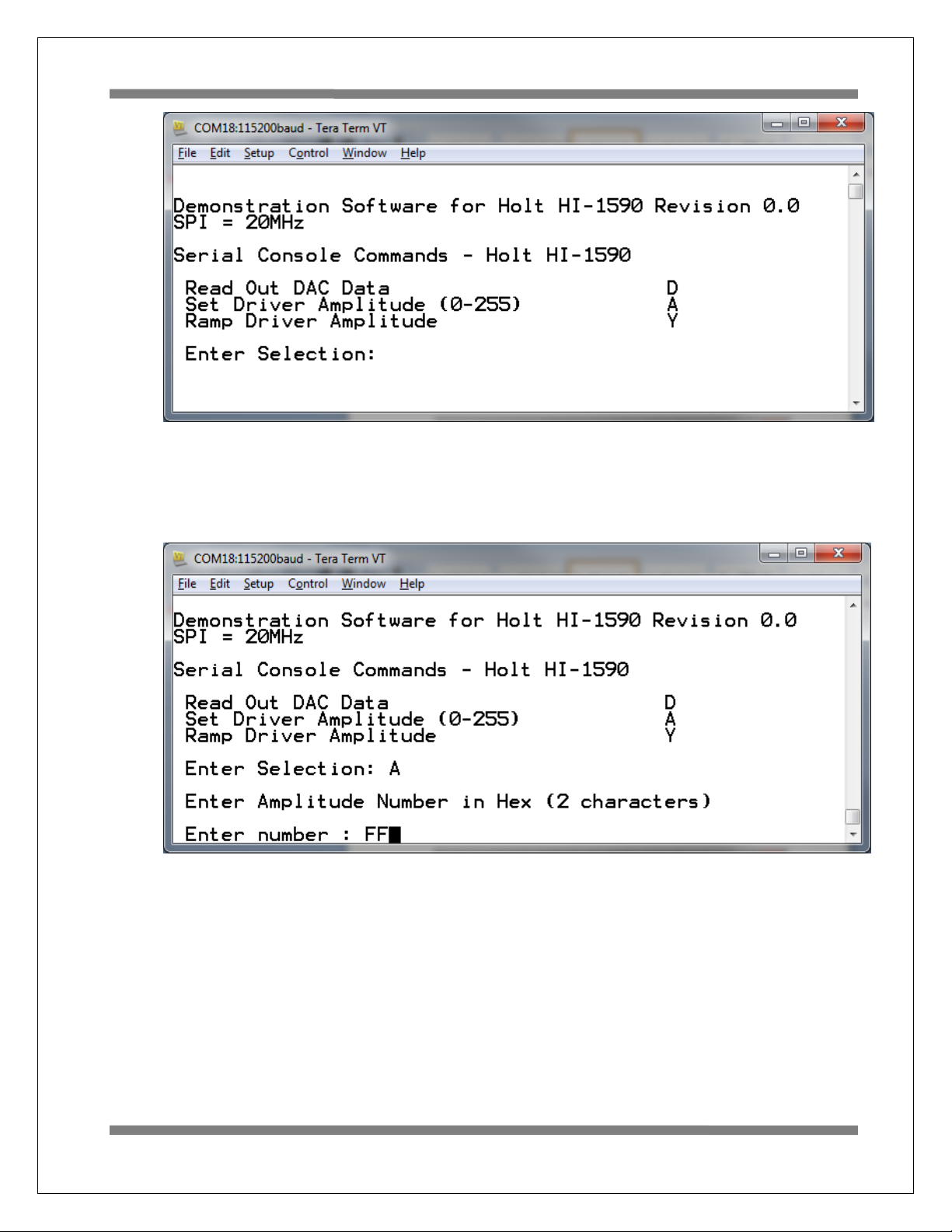
4. The evaluation software is preprogrammed into the microcontroller and was loaded at the
Holt Applications Support Center. On pressing the ‘RESET MICRO’ button on the board, the
software displays a message on the monitor, as shown below.

AN-1590
9 Holt Integrated Circuits
Note: If under any circumstances the software locks up, use the ‘RESET’ key to restart.
5. Press the ‘A’ key to set the output amplitude. Enter the maximum amplitude of ‘FF’ as shown
below.
6. Connect an oscilloscope to the ABUS and BBUS terminal, with the grounds going to nABUS
and nBBUS respectively. Grounding the negative bus terminals provides differential voltage
measurements using just one scope probe per bus. Trigger the scope from the ACTIVE test
point. Press the STOP button, this loads the 1553 messages. Press the RUN button to start
message transmission. The messages will be transmitted alternately on the A and B buses.
Check that a 1553 signal of about 24V p-p amplitude is seen on one of the buses, as shown in
Fig 2 below. Every 5 seconds it will switch to the other bus and during transmission you
should see the 3.3V supply current go up to about 1A.

AN-1590
10 Holt Integrated Circuits
Fig 2: Yellow is BUSA output, green is BUSB, Red is the ACTIVE trigger signal
7. The HI-1590 can also read back data from the DAC register but only after a value has been
written into the register. Press the ‘D’ key, type in ‘80’, the previous setting of ‘FF’ should be
read out as shown below. Observe the amplitude on the scope; this should be reduced by
half, or approximately 12V p-p.
8. The SPI software has a ramp function, this ramps the amplitude on both outputs up to
maximum and back down to zero in a ‘sawtooth’ function. Press the ‘Y’ button and observe
the amplitude rising and falling. Whilst in this mode switch the VSEL switch to ‘Low’, this
selects the low amplitude, you should see the oscilloscope trace go down to one fifth
maximum amplitude or about 5V.
9. As well as SPI control of amplitude through a DAC, the HI-1590 has the option of using an
analog voltage of 0 to 3.3VDC to control the amplitude. To use this feature move the jumper

AN-1590
11 Holt Integrated Circuits
link from J5 to J4. Now amplitude is controlled by potentiometer R3, turn fully clockwise for
maximum amplitude. An external voltage can be used by removing the J4 jumper and
applying the voltage to pin 2 of J4. The range is 0 to VLOGIC (3.3V nominal)
10. To test HI-1590 BusA and BusB receivers, RXENA and/or RXENB switches should be in the
high position. Any 1553B compliant data is now output on the relevant RXA/nRXA and
RXB/nRXB pins of J3. An example is shown in Fig 3 below:
Fig 3: Yellow is BUSA output, green is RXA output, Red is the ACTIVE trigger signal
11. If isolation of the 1553B outputs is required from the board ground the soldered jumpers
JP11 and JP12 should be opened.

AN-1590
12 Holt Integrated Circuits
Appendix 1 Demo software overview
This overview flow chart shows the demo program at a glance.
Display Control
Menu
Valid function
selected?
Main.c Start
Initialize global variables + arrays
Initialize Peripherals
Initialize Interrupts
Initialize Timer
Configure MCU SPI bus
Configure UART
Set SPI clock rate
Display console header
N
Y
Scan Keyboard
for Menu Selection
Case D Y
N
SPI byte write to
amplitude register
and read back
previous setting
Case A
Y
N
SPI byte write to
amplitude register
Case Y
Y
N
Enter Ramp
Amplitude Loop
At reset the program initializes the variables and configures the peripherals including the SPI block,
Timers, Interrupts and serial communication UART. The program then enters Serial Command mode,
this is an endless loop that continuously samples the keyboard. Once a key is pressed the
The program enters a case function that selects which function to call.

AN-1590
13 Holt Integrated Circuits
There is one write function that just writes a byte to the amplitude control register, a read function that
writes data to the amplitude register whilst simultaneously reading back the previous byte. The third
function is a loop that ramps up the amplitude to maximum and then ramps down, taking about 4 secs
to complete this cycle. This last function is an endless loop that is interrupted by pressing any key.
MCU Clock and SPI Frequencies
The Freescale MC9S12XDT512 (MCU) on the main board uses a 4MHz crystal for operation and the built-
in PLL multiplies this by 20 to achieve an 80MHz system clock. This system clock is divided by two for a
40MHz Bus Clock, used internally for the MCU peripherals.
The PLL is programmed to multiply by 20 by this line of code in the Peripherals.c module:
SYNR = 9; // 80MHz PLL system clock
The SPI frequency is set at the beginning of the main.c module, by this code :
SPI0BR = 0x00; // 20MHz SPI
// SPI0BR = 0x01; // 10MHz SPI
// SPI0BR = 0x02; // 5MHz SPI
The speeds that are not used are commented out. In this case the 10MHz and 5MHz are commented
out, so the 20MHz option is set. The maximum SPI frequency for the HI-1590 is 20MHz, the code can be
altered to set a lower rate of 10MHz or 5MHz, if desired.
Timing and Delay Functions
These functions provide the basic timing for the program. The Delay100us() can be used anywhere an
accurate delay is needed in the program .
The global g_count100us variable is decremented at the 100us timer rate. This variable is used by a
general delay function which can be called with a specified number of delay intervals. The g_count100us
variable is a 16-bit integer so the delay ranges from 100us to 6.5536 seconds.
// --------------------------------------
// General timer tick 100us for delays
// --------------------------------------
void Delay100us(unsigned int delay){
g_count100us=delay;
while(g_count100us);
}

AN-1590
14 Holt Integrated Circuits
SPI Driver Functions
Only one SPI function is used, trx8bits_8, shown the figure below:
SPI Read/Write Function
Return rxbyte
Transmit byte whilst
clocking in receive data
Received
Byte ?
No
Yes
Txrx8bits_8
Clear SPI status reg
Load SPI data reg with cmd
Only single-byte transfers are used on the HI-1590, this HI-1590 SPI driver function is included in the
Driver.c module and its Driver.h header file. The MCU slave select pin SSO (not nCS) is connected to the
HI-1590 nCS pin.
Uart.c Serial Port
The drivers supporting the USB serial port (console) are contained in this module. Some function drivers
allow messages to be sent and received on the UART. This is useful to log status or data messages on
HyperTerminal or any other terminal program. It currently uses polling to determine when the data
receive or transmit registers can be read or written.

AN-1590
15 Holt Integrated Circuits
HI-1590 demo Codewarrior Software Project
The software project is built with Freescale’s CodeWarrior version 5.9.0 using the free limited 32K
version. The current code size of the demo is approximately 10K. The main functions are in main.c and
the low level drivers are in the driver.c file. The software project “HI-1590 Demo x_x” will normally be
distributed in a zip file on a CD-ROM with the same name. To develop, debug and download this
software into the board, a PE Micro “USB Multilink Interface” debug cable is necessary. It is not
provided in this kit. To purchase this cable, go to the PE Micro website or purchase it from DigiKey. See
the links at the end of this document.
Project Files
Source Files
main.c Main code
Driver.C SPI low-level driver for the HI-1590
peripherals.c Micro GPIO, PLL frequency and SPI configuration
Uart.c Low-level UART drivers
datapage.c Freescale IDE support file
Include Files
main.h
Driver.h
peripherals.h
Uart.h
common.h Common defines for the project
derivative.h Freescale IDE support file
mc9s12xdt512.h Freescale IDE target part support file

AN-1590
16 Holt Integrated Circuits
CodeWarrior and Software Project Installation:
1. Download and install the CodeWarrior IDE from the Freescale website. The download links are
provided below.
2. Unzip the HI-1590 x_x zip file into the directory you plan to use for your project.
3. Navigate to the HI-1590 project folder and double click the HI-1590 Demo x_x.mcp project file to
launch this project with CodeWarrior. The IDE should open with the project files on the left side
of the window, as shown below:
4. Plug the USB Multilink 6-pin debug cable into the Debug Header and power up the board with
3.3V.
5. Click the green arrow on the screen to ‘build’ the Project . The project should build without
errors. You may receive a dead assignment warning if for example some defines are set to a zero
value. Once built, it should launch the debugger and download to the board.

AN-1590
17 Holt Integrated Circuits
6. The first time you download, you may need to configure the debugger for the USB Multilink
cable. After downloading is complete the debugger window should be displayed with the first
line in main.c highlighted. Press the green horizontal arrow button to run the program. Since the
program has been loaded you can power down the board and re power the board and the
program should run automatically without the debugger. Holt HI-1590 project loaded with
CodeWarrior 5.9.0.

PCB P/N: HV001
Rev. B Bill of Materials
HI-1590 Variable Amplitude Dual 1553 Transceiver Evaluation Board
March 15, 2018
Item Qty Description Reference DigiKey Mfr P/N
1 1 PCB, Bare, Eval Board Jet Tech 37850
219
Capacitor, Cer 0.1uF 20% 50V Z5U 0805
C1,C3,C6,C7,C8,C10-
C13,C15,C17- C21,C23-C26
399-1176-1-ND
Kemet C0805C104M5UACTU
3 6 Capacitor, Cer 220nF 10% 50V X7R 0805 C29,C30,C34,C37,C38,C39 399-3491-1-ND Kemet C0805C224K5RACTU
4 2 Capacitor, Cer 10pF 50V 5% NPO 0805 C28,C31 399-1108-1-ND Kemet C0805C100J5GACTU
5 2 Capacitor, Cer 47pF 50V 5% NPO 0805 C32,C33 399-1117-1-ND Kemet C0805C470J5GACTU
6 1 Capacitor, Cer 470pF 50V 5% X7R 0805 C36 399-1133-1-ND Kemet C0805C471J5GACTU
7 2
Capacitor, Cer 0.01uF 20% 50V 7XR 0805 C27,C35 399-1160-1-ND Kemet C0805C103M5RACTU
8 1
Capacitor, Cer 4.7uF 10% 6.3V X5R 0805 C16 399-3134-1-ND Kemet C0805C475K9PACTU
9 1 Capacitor, Cer 4.7uF 10V 10% X5R 1210 C4 587-1379-1-ND Taiyo Yuden LMK325BJ475KD-T
10 1
Capacitor, Cer 47uF 10V 20% X7R 1210 C5 587-2783-1-ND Taiyo Yuden LMK325B7476MM-TR
11 3
Capacitor 68uF 10% 6.3V Tant 400 mOhm
SMD EIA 2312
C2,C9,C14 399-10513-1-ND Kemet T495C686K006ATE400
12 1
Capacitor 68uF 10% 16V Tant 400 mOhm
SMD EIA 2917
C22 399-8397-1-ND KemetT491D686K016AT
13 2
Connector 3-Lug Concentric Triax Bayonet
Jack, Panel Front Mount TRB (BJ77)
J1,J2 ** MilesTek 10-06570 Trompeter Electronics BJ77
14 1Connector, Receptacle USB Mini B R/A J9 H2959CT-ND Hirose UX60-MB-5ST
15 1Header, Female, 30 Pos 0.1" Pitch, R/A J7 S5568-ND Sullins PPPC152LJBN-RC
16 1Header, Female, 6 Pos 0.1" Pitch, R/A J11 S5517-ND Sullins PPTC032LJBN-RC
17 1
Header, Male 2x8 0.1" Pitch, 0.230" Pins J10 S2012E-08-ND Sullins PEC08DAAN
18 1Header, Single 1x4, 0.1" pitch J6 OPTIONAL S1012E-04-ND Sullins PEC04SAAN
19 3Header, Single 1x2, 0.1" pitch J4,J5,J8 S1012E-02-ND Sullins PEC02SAAN
20 1Shunt Connector Black J4 S9000-ND Sullins STC02SYAN
21 1Header, single 1x4, 0.2" pitch J3* S1012E-07-ND Sullins PEC07SAAN
22 12 Solder Jump 2 terminals JP1-JP12 OPEN
23 1Solder Jump 3 Terminals J12 OPEN
24 1LED Green 0805 ACTIVE 160-1179-1-ND LiteOn LTST-C170GKT
25 1LED Red 0805 POWER ON 160-1178-1-ND LiteOn LTST-C170EKT
26 2Resistor, 69.8 Ohm 1W 1%, 2512 R1,R2 RHM69.8BBCT-ND Rohm MCR100JZHF69R8
27 1Trim Pot 1K - 3/4 Turn w/ Knob R3 3386P-102TLF-ND Bourns 3386P-1-102TLF
28 2Resistor, 27 5% 1/8W 0805 R20,R22 P27ACT-ND Panasonic ERJ-6GEYJ270V
29 1Resistor, 150 5% 1/8W 0805 R10 P150ACT-ND Panasonic ERJ-6GEYJ151V
30 1Resistor, 330 5% 1/8W 0805 R15 P330ACT-ND Panasonic ERJ-6GEYJ331V
31 1 Resistor, 1K, 1/8W 5% 0805
R5 P1.0KACT-ND Panasonic ERJ-6GEYJ102V
32 3 Resistor 3.3K, 1/8W 5% 0805
R18,R19,R24 P3.3KACT-ND Panasonic ERJ-6GEYJ332V
33 1 Resistor, 4.7K, 1/8W 1% 0805 R23 P4.7KACT-ND Panasonic ERJ-6GEYJ472V
34 2Resistor, 10K 5% 1/8W 0805 R11,R14 P10KACT-ND Panasonic ERJ-6GEYJ103V
35 5Resistor, 47K 5% 1/8W 0805 R6,R7,R8,R9,R16 P47KACT-ND Panasonic ERJ-6GEYJ473V
36 2Resistor, 100K 5% 1/8W 0805 R12,R13 P100KACT-ND Panasonic ERJ-6GEYJ104V
37 1Resistor, 220K 5% 1/8W 0805 R17 P220KACT-ND Panasonic ERJ-6GEYJ224V
38 1 Resistor, 1M, 1/8W 5% 0805 R21 P1.0MACT-ND Panasonic ERJ-6GEYJ105V
39 1Ferrite Bead, 220 Ohm 300mA 0805 FB1 732-1602-1-ND Wurth 742792034
40 1Ferrite Bead 330 Ohm 1.5A 0805 L1 490-5988-1-ND Murata BLM21PG331SN1D
41 1Osc, 50MHz 100ppm 3.3V SMD 5x7mm OSC1 535-10087-1-ND Abracon ASV-50.000MHZ-E-T
42 1 Crystal 4.00MHz, SMD, 30ppm 20pF load Y1 631-1005-1-ND FOXSDLF/040
43 2DIP Switch 5-Position SMD SW1,SW5 CT2195MST-ND CTS 219-5MST
44 1DIP Switch 6-Position SMD SW6 CT2196MST-ND CTS 219-6MST
45 3 Switch Tactile SPST-NO 0.05A 32V SW3,SW4,SW7 P12943SCT-ND Panasonic EVQ-Q2K03W
46 3Test Point, Red Insulator, 0.062" hole 3V3,ABUS, BBUS 36-5010-ND Keystone 5010
47 3
Test Point, Black Insulator, 0.062" hole GND, nBusA, nBusB 36-5011-ND Keystone 5011
48 3Solid wire, 20 AWG, 3" Long per Board GND Hookup 20WG Solid wire Any 20 AWG Solid Wire
49 1
Test Point, Orange Insulator, 0.062" hole VDD 36-5013-ND Keystone 5013
50 1
Test Point, White Insulator, 0.062" hole ACTIVE 36-5012-ND Keystone 5012
51 1
IC, MC9S12XDT512CAA 80QFP,16-Bit MCU, 512K,Flash 0-70C
U5 MC9S12XDT512CAA-ND MC9S12XDT512CAA-ND
52 1IC USB Serial Full UART 20SSP U6 768-1129-1-ND FTDI FT231XS-R
53 2
IC, Serial EEPROM 512Kbit 20MHz SPI
8-SOIC, Microchip
U2,U4 25LC512-I/SN-ND Microchip 25LC512-I/SN
54 2
TVS, Diode 5VWM 14VC SOT23 DN1,DN2 D5V0L2B3SO-7DICT-ND Diode Inc. D5V0L2B3SO-7
55 1IC HI-1590 44QFN U1 HOLT IC Holt IC
56 1IC HI-6131 64-PQFP U3 HOLT IC Holt IC
57 2
Transformer MIL-STD-1553 Single, 1:2.50,
PM-DB2791S
T1,T2 PM-DB2791S
Holt / Premier Magnetics PM-
DB2791S
58 6
Stand-off, #4-40 Female Thread, 3/4" long 3481K-ND Keystone 3481
59 6
Machine Screw, #4-40 x 1/4" H342-ND B&F Supply PMS 440 0025 PH
60 6Lock Washer, Int.Tooth #4-40 H236-ND B&F Supply INTLWZ 004
61 4
Hookup Solid wire - 20AWG - Black - 4"
Long per Board
For J1 and J2 C2028B-XX-ND General Cable C2028A.12.01

5
5
4
4
3
3
2
2
1
1
D D
C C
B B
A A
RED
BUS NOT CONFIGURED
TO TEST DIRECT-COUPLED,
NO SERIES RESISTORS.
LOCATE
C3 CLOSE
TO PIN 12.
GND
GND
<---- CW
RED
BUSB
LOCATE
C1 AT
PIN 6.
BLK
1
0
VSEL
1
3
2
1
3
2
BLK
BUSA
VSEL
TXB
nTXB nTXA
TXA
B
RXB
nRXB
RXA
nRXA
SCK
nCS
SI
SO
3V3
nTXB
TXB
TXA
nTXA
GND
Title
Size Document Number Rev
Date: Sheet of
<Doc>
HI-1590 1553 Dual Transceiver
A
1 3Thursday, March 15, 2018
Title
Size Document Number Rev
Date: Sheet of
<Doc>
HI-1590 1553 Dual Transceiver
A
1 3Thursday, March 15, 2018
Title
Size Document Number Rev
Date: Sheet of
<Doc>
HI-1590 1553 Dual Transceiver
A
1 3Thursday, March 15, 2018
TP6
TP25
C5 47uF
R3 1K
TP3
C6
100nF
C3
100nF
R7
47K
JP9
JP3
+
C2
68uF
J3
Header 1x4, 0.2" PITCH
1
2
3
4
TP4
R1
70 1W
TP7
JP12
JP1
TP22
T2
PM-DB2791S
4
5
6
7
8
1
2
3
T1
PM-DB2791S
4
5
6
7
8
1
2
3
TP8
JP8
JP16
nTXA
J1
C4
4.7uF
TP24
JP7
JP2
U1
HI-1590 PQI
N/C 1
RXENA 2
GND 3
GND 4
GND 5
VDD 6
VDD 7
BUSB 8
BUSB 9
BUSB 10
BUSB 11
VDD
12
CAP
13
CAP
14
CRES
15
RXBEN
16
GND
17
GND
18
GND
19
RXB
20
RXB
21
VSEL
22
NC
23
TXINHB
24
TXB
25
TXB
26
N/C
27
N/C
28
RXA
29
RXA
30
TXINHA
31
SCK
32
CSN
33
SO 34
SI 35
TXA 36
TXA 37
VCONT 38
VCONT 39
BUSA 40
BUSA 41
BUSA 42
BUSA 43
N/C 44
JP15
TXA
R5
1K
DN1D5V0L2B3SO
R2
70 1W J2
TP1
JP4
R8
47K
R6
47K
JP6
DN2
D5V0L2B3SO
J4
1 2
JP14
nTXB
TP2
JP5
TP23
R4
0 OHM
JP10
3
21 4 5
ON (CLOSED)
SW1
JP13
TXB
TP5
J5
12
R9
47K
C1
100nF
JP11
nABUS
A8
A4
ABUS
A7
A5
RXB
RXA
nRXA
nRXB
nBBUS
nABUS
TXIHA
TXIHB
3V3
RXBEN
B8
B4
B7
B5
nBBUS
BBUS
VCONT
3V3
RXBEN
RXAEN
TXIHB
TXIHA
nBUSA
BUSB
3V3
3V3
GND
RXAEN
In_nTXA
In_TXA
In_TXB
In_nTXB
In_TXB
In_nTXB
In_TXA
In_nTXA
nBUSB

5
5
4
4
3
3
2
2
1
1
D D
C C
B B
A A
MODE = 0 (EXT TRANSCEIVER)
COMP = 0 (NO PIN, INT PULL-DN)
TEST = 0 (NORMAL)
DECOUPLING
U3 PINS 8, 21, 50, 60
IRQ
RUN
GND
POWER
DECOUPLING
U3 PINS 39, 42
STOP
ACTIVE
GND
1
0
RT MESSAGES - 2 & 3
BC MESSAGES - 1 & 2
3V3 3V3
3V3
3V3
3V3
3V3
TXA
TXB
nTXB
nTXA
RXA
nRXA
RXB
nRXB
nMR
BCTRIG
3V3
GND
Title
Size Document Number Rev
Date: Sheet of
<Doc> B
HI-1590 Dual 1553 Transceiver with SPI Demo Board - Message Generator
A
2 3Thursday, March 15, 2018
Title
Size Document Number Rev
Date: Sheet of
<Doc> B
HI-1590 Dual 1553 Transceiver with SPI Demo Board - Message Generator
A
2 3Thursday, March 15, 2018
Title
Size Document Number Rev
Date: Sheet of
<Doc> B
HI-1590 Dual 1553 Transceiver with SPI Demo Board - Message Generator
A
2 3Thursday, March 15, 2018
U3
HI-6131 PQFP
BCTRIG
1
RAMEDC
2
CE
3
MODE
4
SI
5
SCK
6
SO
7
VDD
8
MCLK
9
GND
10
RT1A0
11
RT1A1
12
RT1A2
13
MR
14
RT1A3
15
RT1A4
16
RT1ENA
17
RT1APAR
18
MISO
19
MOSI
20
VDD
21
GND
22
TTCLK
23
MTTCLK
24
ECS
25
EECOPY
26
ESCLK
27
MTRUN
28
T7
29
T6
30
T5
31
T4
32
T3 33
T2 34
T1 35
T0 36
BUSB 38
VDD 39
BUSB 40
BUSA 41
VDD 42
BUSA 43
BCENA 44
MTSTOFF 45
RT1LOCK 46
TEST 47
BENDI 48
GND 49
VDD 50
IRQ 51
ACKIRQ 52
RT1MC8 53
RT2MC8 54
MTPKRDY 55
READY 56
ACTIVE 57
RT1SSF 58
GND 59
VDD 60
AUTOEN 61
TXINHA 62
TXINHB 63
NC 64
RT2ENA 37
R13
100K
C17
100nF
C13
100nF
C12
100nF
TP9 TP10
J6
Header 1x4
1
2
3
4
C20
100nF
OSC1
50.0MHz
OE
1
GD
2OUT 3
VCC 4
3
21 4 5
ON (CLOSED)
SW5
R15
330
TP11
J7
EEPROM LOAD
1 2
3 4
5 6
7 8
9 10
11 12
13 14
15 16
17 18
19 20
21 22
23 24
25 26
27 28
29 30
SW3
U4 25LC512 8-SOIC
CS
1
SO
2
WP
3
GND
4SI 5
SCK 6
HOLD 7
VCC 8
+
C14 68uF
R11 10K
C18
100nF
C10
100nF
R10
150
C11
100nF
C19 100nF
R14 10K
U2 25LC512 8-SOIC
CS
1
SO
2
WP
3
GND
4SI 5
SCK 6
HOLD 7
VCC 8
TP13
TP14
C15
100nF
R12
100K
+
C9
68uF
3
21 4 5 6
ON (CLOSED)
SW6
+
C16
4.7uF
C7
100nF
J12
CON3
1
2
3
LED1
R16
47K
C8
100nF
SW4
LED2
GNDGND
3V3
nECS
EECOPY
ESCK
GND
3V3
EMOSI
EMISO
RT1AP
RT1ENA
nECS
3V3
ESCK
RT1A0
RT1A1
RT1A3
RT1A4
RT1A2
RT1AP
EMISO
GND
3V3
GND
EMOSI
GND
GND
3V3
3V3
BCENA
RT1LOCK
ESCK
EMOSI
GND
ACTIVE
READY
3V3
GND
AUTOEN
GND
3V3
GND
GND
3V3
GND 3V3
EMISO
nMR
EMOSI
ESCK
EMISO
nECS
3V3
3V3
GND
BCTRIG
MOSI
MSCK
RT1A0
RT1A3
RT1A2
RT1A4
RT1A1
nMR
MISO
3V3
GND
MCLK
nPCS0
ACTIVE
GND
AUTOEN
3V3
RT1LOCK
BCENA
RT1ENA
CPYRQ
nPCS0
3V3
BCENA
nMR
AUTOEN
CPYRQ
EECOPY
MISO
READY
3V3
RT1ENA
MSCK
3V3
MOSI
3V3
GND
nECS1
nECS2
Other manuals for HI?1590
1
This manual suits for next models
1
Table of contents
Other HOLT Motherboard manuals
Popular Motherboard manuals by other brands

Texas Instruments
Texas Instruments LP5012EVM user guide

IEI Technology
IEI Technology Kino-g410 user manual

Texas Instruments
Texas Instruments TPSM8D6C24EVM-2V0 user guide

Gigabyte
Gigabyte GA-H61M-DS2 DVI user manual

Semtech
Semtech LoRa Edge Tracker Reference Design Evaluation... user guide

ON Semiconductor
ON Semiconductor CAT4201 manual