HOLT ADK-25850FMC User manual

QSG-25850FMC Rev. B Holt Integrated Circuits
ADK-25850FMC Quick Start Guide –
Dual HI-25850 Transceiver
FMC Demonstration
Board
February 2023

QSG-25850FMC
QSG-25850FMC Rev. B Holt Integrated Circuits
2
REVISION HISTORY
Revision Date Description of Change
QSG-25850FMC Rev. New 09/08/2020 Initial Release.
Rev. A 05/30/2021
Update BOM for both boards. Minor update to
schematic.
Rev. B 02/10/2023 Update for new board with pinout changes.

QSG-25850FMC
QSG-25850FMC Rev. B Holt Integrated Circuits
3
Introduction
The Holt ADK-25850FMC is a dual channel MIL-STD-1553 transceiver FPGA Mezzanine Card (FMC)
populated with one or two Holt HI-25850 121 BGA dual redundant transceivers. The FMC card uses the
standard IAW VITA 57.1 form factor. The user has the choice to use the FMC connectors or two PMOD
connector headers for interfacing to a host or FPGA. The HI-25850 transceiver used on this card is
essentially a HI-15850 transceiver with integrated transformers configured with a Transformer Coupled
interface. The card is available in a single channel configuration ADK-25850FMC-1, or a dual channel
configuration ADK-25850FMC-2.
Figure 1 - ADK-25850FMC-2 – 2 Channel MIL-STD-1553 FMC Demonstration Board

QSG-25850FMC
QSG-25850FMC Rev. B Holt Integrated Circuits
4
Figure 2 - ADK-25850FMC MIL-STD-1553 cable assembly (only one shown, -2 includes two sets).
Features:
•One or two channel HI-25850 dual redundant MIL-STD-1553 transceivers
•FPGA Mezzanine Card; VITA 57.1
•FMC or PMOD connectivity
•DIP switches and jumpers configuration options
•One or two MIL-STD-1553 cable assemblies
•External power supply option connector
ADK-25850FMC Contents:
•One or two channel HI-25850 FMC card
•One or two D type MIL-STD-1553 cable assemblies
•5V, 2A power adapter with USB 2.0 cable
•Quick Start Guide

QSG-25850FMC
QSG-25850FMC Rev. B Holt Integrated Circuits
5
Interface Voltage Selection.
The HI-25850 devices allow for 1.8V, 2.5V or 3.3V logic levels to ease interfacing to a wide variety of
FPGA’s or other host logic. Configure J9 jumper header according to the desire voltage. A VDDIO test
point is provided so a meter could be used to verify the voltage prior to use.
CAUTION: ENSURE THE PROPER VOLTAGE IS SELECTED FOR THE TARGET FPGA. IF THE HOLT
CARD VOLTAGE DOES NOT MATCH THE HOST/FPGA, DAMAGE TO THE FPGA OR HOLT CARD
MAY OCCUR.
Table 1 - Digital I/O Voltage Selection using Jumper J9
1.8V
2.5V
3.3V
J9 1-2
J9 3-4
J9 5-6
Power Supply Considerations and Selection.
3.3V power to the HI-25850 is jumper selectable between the FMC connector or from the two PMOD
connectors. For optimum performance, all grounds and 3.3V pins on the PMOD connectors are
recommended in order to minimize IR voltage drops when the transceivers transmit data.
3.3V power is selectable from either the FMC connectors or from on-card 3.3V voltage regulators. Power
to these voltage regulators are supplied by an external 5V power adapter. A MOSFET switches power to
the regulators when 3.3V is powered in order to provide timed power sequencing. The default is
configured for FMC power.
Table 2 - Transceiver Power Routing
Transceiver Power routing
FMC - Default
External 5V Adapter
25850 U1
JP19
JP12
25850 U2
JP110
JP11
Note: only one source jumper should be used for each IC.
If the FPGA FMC power source is sufficient to power both devices this is the recommended
configuration, otherwise one or both devices can be powered by the external 5V adapter. Each HI-25850
can draw up to 900mA when transmitting 100% duty, during idle the current will drop down to 40—

QSG-25850FMC
QSG-25850FMC Rev. B Holt Integrated Circuits
6
50mA. See pages 11 and 12 of the data sheet for more information on current and power dissipation of
these devices.
Figure 3 - HI-25850 Block Diagram
Note: Figure 3 Transceiver Block Diagram is showing BusA only
Bus Receive Signal Path
A pair of CMOS logic-levels depending on the voltage selected by J9 (1.8V, 2.5V or 3.3V) provides bipolar
serial signals for connecting each bus to an external user-provided Manchester decoder. RXA and nRXA
are the non-inverted and inverted receiver outputs for Bus A; RXB and nRXB are the receiver outputs for
Bus B. The logic-level Bus A and Bus B receiver outputs can be enabled/disabled using the transceiver
RXENA and RXENB inputs.
The RX and nRX receive outputs have an option to stretch minimum output pulse width. When receiving
differential signals near the MIL-STD-1553 minimum amplitude specification (860 mVpp or less when

QSG-25850FMC
QSG-25850FMC Rev. B Holt Integrated Circuits
7
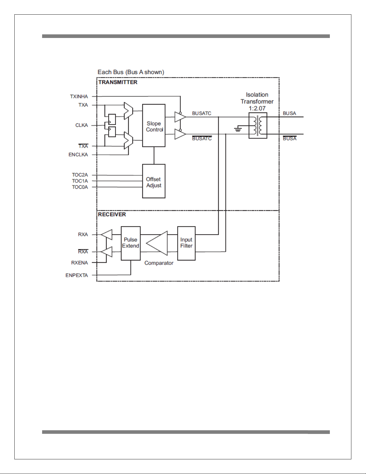
transformer-coupled), traditional transceivers produce narrow output pulses at RX and nRX because the
time that analog bus voltage exceeds the receiver threshold is much shorter than for a nominal or large
amplitude bus voltage. This function is enabled by opening SW1 or SW3 DIP switches which will assert
highs on the ENPEXTA and ENPEXTB pins of each device due to internal pull-ups. When these pins are
low, the comparator output is conventional.
Figure 4 - Bus Receiver Signal Path
Note: Receiver pulse stretching may cause issues with noise rejection, especially when noise pulses are
stretched in the intermessage gap just before or during command sync rising edge. For this reason, use
of receiver pulse width stretching should be weighed carefully against noise immunity considerations.
Bus Transmit Signal Path
A pair of CMOS logic-level inputs accepts bipolar serial signals for driving each bus from an external user-
provided Manchester encoder. Transmit for each bus can be enabled or inhibited using the
corresponding TXINH transmit inhibit signal.
The transmit signal path for each bus includes the bipolar TX and nix signals generated by the external
Manchester encoder. Signal quality concerns dictate that the TX/nix signals for each bus have matched
characteristics. This includes matched conductor length and impedance, matched layer-to-layer vias (or
even better, no vias). It is not always possible to achieve good matching on the board layout. The result:
TX and nTX switching transitions are not quite simultaneous; the TX/nTX crossover occurs early or late.
Crossover should occur mid-way between ground and the VDDIO supply rail to assure acceptable
“output symmetry” or “tail-off” occurring at the end of long transmit messages. This effect is discussed
at length in Holt application note AN-550.
Transmit Signal Sync Option
To accurately synchronize TX and nTX inputs, the HI-25850 offers the option to simultaneously clock
transmit input signals for each bus with a clock pulse input pin. When high, the CLKAEN input enables
synchronized TX and nTX inputs for bus A. With synchronization enabled (CLKENA = 1), the CLKA input
pin synchronizes TXA and nTXA for bus A transmit. If using an FPGA encoder, the user must provide a
brief positive clock pulse every time the TXA and nTXA signals change state. Logic levels present at the
TXA and nTXA inputs are latched by CLKA rising edge. If CLKENA is held low, the clocked input latches are
bypassed and the CLKA input has no effect.

QSG-25850FMC
QSG-25850FMC Rev. B Holt Integrated Circuits
8
Similarly, CLKENB enables or disables synchronized operation for bus B, accomplished using the TXB,
nTXB and CLKB inputs. The CLKENA and CLKENBA input pins have weak pull-down resistors.
DIP switches are provided to set the CLKENA or CLKENB signals high or low. Refer to table 1.
Bus Tail-Off Trim
On DIP switch package SW2 and SW3, switches labeled TOC0A, TOC1A and TOC2A are used in
combination to provide up to +180mV or -180mV DC tail-off adjustment on Bus A, to compensate for a
board layout deficiency that causes chronic, consistent tail-off which would benefit from an across-the-
board fixed amplitude adjustment. The TOC switch settings select one of six correction levels. There are
two “no correction” TOC combinations. Table 2 on page 8 in the HI-25850 data sheet summarizes the
TOC switch combinations. Figures 4 and 5 in the data sheet show examples of various applied correction
levels.
Tail-off trim for Bus B works similarly using switches labeled TOC0B, TOC1B and TOC2B on DIP switch
package SW2. All TOC input pins have weak pull-down resistors that present logic-0 when the
corresponding DIP switches are open.
Transformer-Coupled Operation
The HI-25850FMC card provides transformer-coupled operation.
A transformer-coupled 1553 bus interface is the predominant configuration used for terminal
connection. This diagram shows a network comprised of three transformer-coupled terminals: a Bus
Controller (BC) and two Remote Terminals (RTs). Stub cables must be < 20 feet (6.1 meters).

QSG-25850FMC
QSG-25850FMC Rev. B Holt Integrated Circuits
9
Figure 5 - MIL-STD-1553 Bus Connections
The HI-25850 Signal Break-Out Board (and user-provided protocol logic) takes the place of the BC or one
of the RTs in the above diagram.
As seen above, each terminal’s stub cable connects to the 1553 bus through a “bus coupler,” which is
typically an off-the-shelf hardware component comprised of coupling transformer(s) for one or more
terminal stubs (each with its own pair of internal current-limiting resistors). Two bus couplers are shown
above. The bus couplers have a bus connection jack at each end for serial connection into the 1553 bus
structure. Each end of the bus has a 78Ω terminator. Holt application note AN-550 provides additional
information about the direct- and transformer-coupled configurations.
Dummy Resistor Bus Load Option
The HI-25850FMC card provides some jumpers or shunt locations to select on-board resistor dummy bus
load or off-board conventional 1553 bus connection, shown above. When enabled, the on-board
dummy load replaces the stub cable assembly in the diagram and everything above it; the resistor load
appears directly at the terminal bus interface. The load is 70Ω for transformer-coupled operation. These
are useful when performing card signal tests such as measuring transmit output Peak-to-Peak voltages
or measuring receiver input sensitivity.

QSG-25850FMC
QSG-25850FMC Rev. B Holt Integrated Circuits
10
Single Scope Probe “Faux Differential” Viewing Option
When characterizing a 1553 terminal, most bus measurements are the differential line-to-line stub
voltage measured across the bus side of the terminal’s isolation transformer. For the HI-25850 signal
card, the transformer secondary’s BUSA/nBUSA and BUSB/nBUSB outputs can be viewed on an
oscilloscope at the test points.
Differential line-to-line voltage measurement for Bus A can be accomplished by connecting oscilloscope
probes for channel 1 and channel 2 to the BUSA and nBUSA test points respectively, and using scope
built-in math function to observe “channel 1 minus channel 2. Jumpers are provided that allow
grounding the negative side of the bus to make measurement of the output easier.
This is strictly a convenience measure to be used when evaluating HI-25850 transceiver performance;
the minus side of the 1553 bus stub would never be left grounded under normal circumstances for
production hardware.
The above comments for configuring Bus A also apply for Bus B, substituting test points BUSB and
nBUSB for test points BUSA and nBUSA respectively.
Table 3 - Jumpers, Swtiches, and Test Points
JP1
U1 BusA
70 ohm test termination
Default Open
JP3
U1 BusB
70 ohm test termination
Default Open
JP5
U2 BusA
70 ohm test termination
Default Open
JP7
U2 BusB
70 ohm test termination
Default Open
JP2
U1 BusA
Test ground nAbus
Default Open
JP4
U1 BusB
Test ground nBbus
Default Open
JP6
U2 BusA
Test ground nAbus
Default Open
JP8
U2 BusB
Test ground nBbus
Default Open
Note: For this Table 3, Channel 0 refers to BusA and BusB on U1, Channel 1 refers to BusA and BusB on
U2. For other power supply related jumpers see Table 1 and Table 2the beginning of this document.

QSG-25850FMC
QSG-25850FMC Rev. B Holt Integrated Circuits
11
Table 4 - 1553 Output bus Test Point Hooks
HK1/HK2
U1 Abus/nAbus
HK3/HK4
U1 Bbus/nBbus
HK5/HK6
U2 Abus/nAbus
HK7/HK8
U2 Bbus/nBbus
Table 5 - Misc. Test Point Hooks
HK9
External 5V adapter input
HK18,19,20
Grounds
HK10
3.3V regulator output for U1
HI11
3.3V regulator output for U2
HK15
VDDIO Voltage going to U1 andU2 (sets the rail
voltage for the host interface.
HK14
1.8V regulator
HK16
2.5V regulator

QSG-25850FMC
QSG-25850FMC Rev. B Holt Integrated Circuits
12
Table 6 - FMC VITA 57.1 FPGA Low-Pin Connector

QSG-25850FMC
QSG-25850FMC Rev. B Holt Integrated Circuits
13
A simple interface
A minimal host interface would require the following signals for a dual redundant MIL-STD 1553
interface.
Table 7 - Simple Host Interface - Signal Descriptions
Signal
HI-25850 (U1 or U2)
TXA
Digital Input. Note 1
nTXA
Digital Input. Note 1
RXB
Digital Output. Note 1
nRXB
Digital Output. Note 1
TXINHA/TXINHB
Transmit Inhibits. Must be low to transmit.
CLKENA/CLKENB
Set low to disable synchronizer.
TXC0A-TXC2A
TXC0B-TXC2B
Set low to disable Bus Tail-Off Adjustments,
both Buses.
VDDA/VDDB
3.3V Power, 900mA (per IC)
VDDIO
Host rail voltage. Set according to FPGA
voltage. See this document. 15mA.
Grounds
All Grounds should be used.
Note 1 – For proper encoder/decoder designs both the normal and semi-complimented signal pairs are
required. The signal pairs are not exactly inverted from each other. See data sheet page 10 for example
waveforms or refer to the diagrams below.
Figure 6 - Transmit Waveform Example
Table of contents
Other HOLT Motherboard manuals