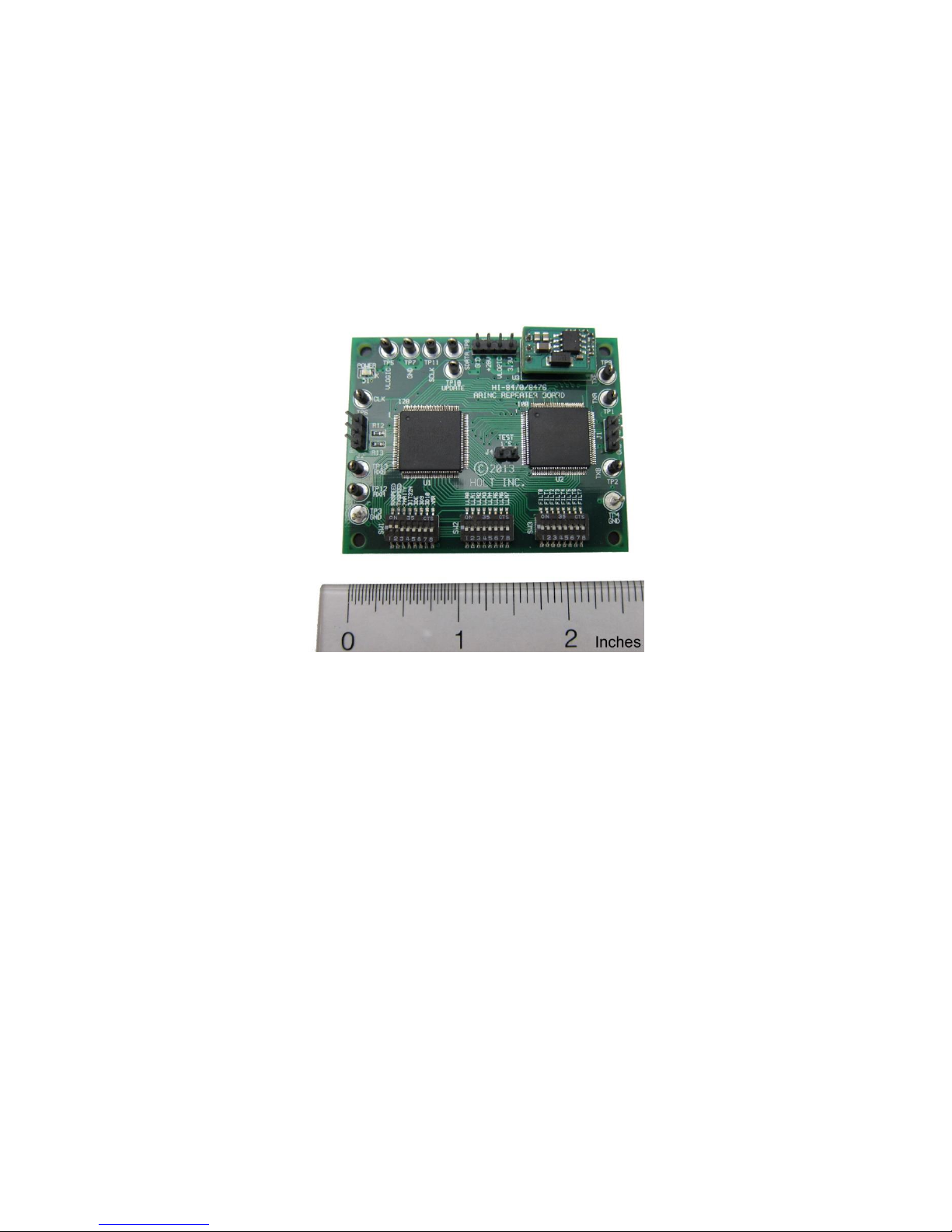
QSG-8476-Repeater_A HOLT INTEGRATED CIRCUITS 10/25/18
6
3. . The ARINC output should now be the same as the ARINC input; the
board is repeating the input signal. Change SW1 TXSPEED to OFF. The output data rate
should be low speed, the data content should be the same as before. Now change SW1
RXSPEED to OFF and input a Low speed ARINC signal, the output data should be the same as
the low speed data input.
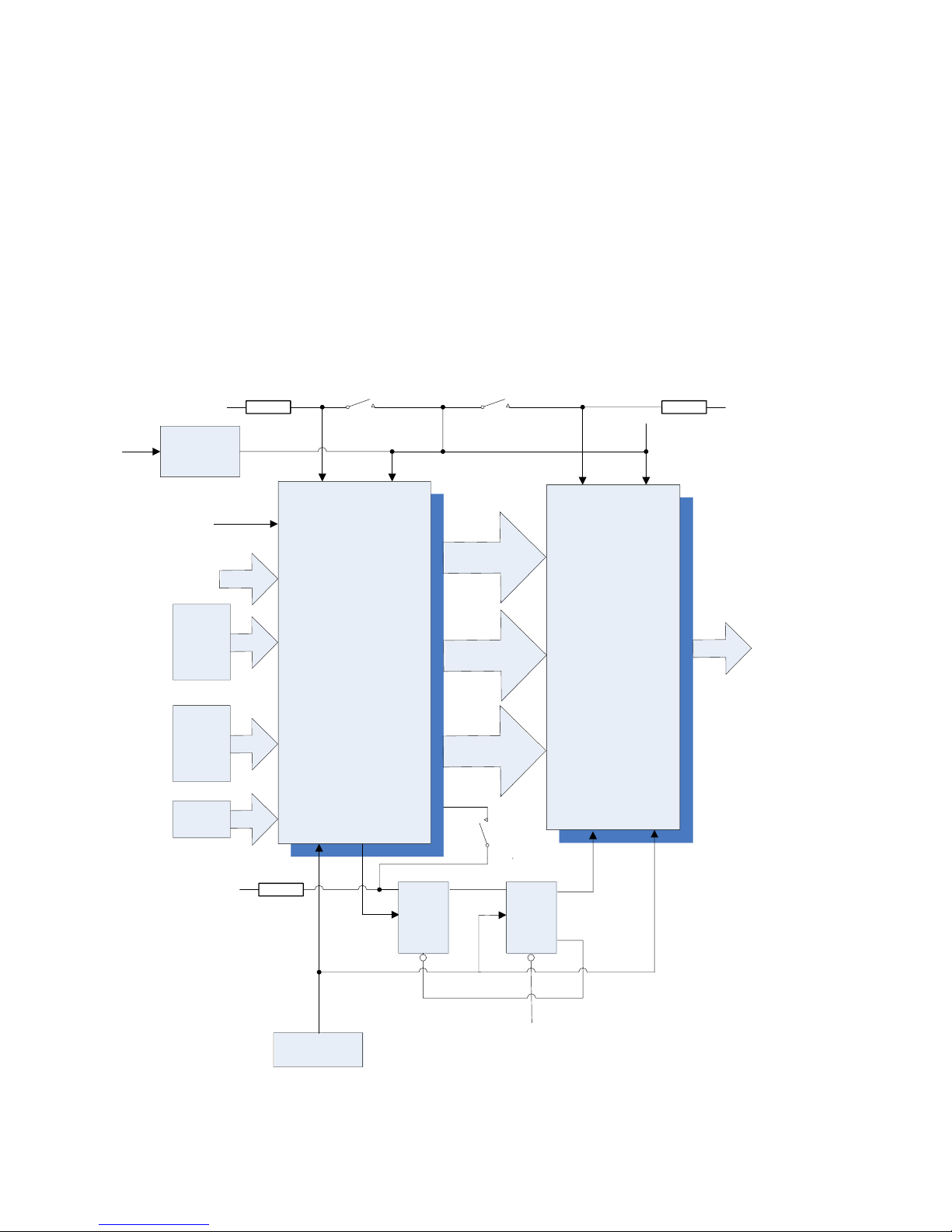
4. If desired, the repeater can selectively repeat ARINC words according to the LABEL content.
The LABEL switch selects the LABEL to be retransmitted and FILT switch selects the LABEL bits
that are evaluated during the filtering process. For example; if only messages with LABEL =
0000001 were required to be repeated, then the LABEL switch SW2 is set to 0000001 and
FILT switch SW3 set to 11111111. Note that on the board the switch bits are in the order of
LSB to the left, MSB to the right. If all words with LABEL bits[1:0] = 11 should be repeated,
then the LABEL switch is set to 00000011 and FILT switch is set to 00000011. In a similar
manner the SD9 and SD10 bits can be used to select word for transmission. See HI-8476
datasheet for more details.
5. With the SW1 PARITY switch in default mode, the repeater will re-transmit all valid ARINC
words whether the parity is odd or even. When set to ON, parity checking is enabled, so only
odd parity words are retransmitted.