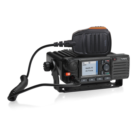
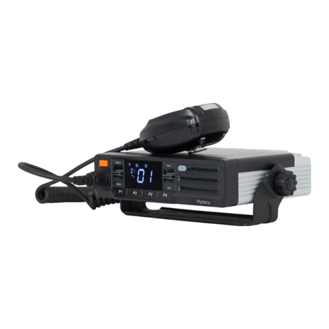
Hytera MD652 User manual

DIGITAL MOBILE RADIO

Preface
This manual describes the information related to the product repair. It is intended for use by qualified
technicians only. To repair the product properly, please read this manual carefully before repairing.
This manual is applicable to the following product:
MD65X Digital Mobile Radio (X may represent 2, 5, 6 or 8)

Copyright Information
Hytera is the trademark or registered trademark of Hytera Communications Corporation Limited (the
Company) in PRC and/or other countries or areas. The Company retains the ownership of its trademarks
and product names. All other trademarks and/or product names that may be used in this manual are
properties of their respective owners.
The product described in this manual may include the Company’s computer programs stored in memory
or other media. Laws in PRC and/or other countries or areas protect the exclusive rights of the Company
with respect to its computer programs. The purchase of this product shall not be deemed to grant, either
directly or by implication, any rights to the purchaser regarding the Company’s computer programs. Any
of the Company’s computer programs may not be copied, modified, distributed, decompiled, or
reverse-engineered in any manner without the prior written consent of the Company.
The AMBE+2TM voice coding technology embodied in this product is protected by intellectual property
rights including patent rights, copyrights and trade secrets of Digital Voice Systems, Inc. This voice
coding technology is licensed solely for use within this product. The user of this technology is explicitly
prohibited from attempting to decompile, reverse engineer, or disassemble the Object Code or in any
other way convert the Object Code into a human-readable format.
U.S. Patent No: #6,912,495 B2, #6,199,037 B1, #5,870,405, #5,826,222, #5,754,974, #5,701,390,
#5,715,365, #5,649,050, #5,630,011, #5,581,656, #5,517,511, #5,491,772, #5,247,579, #5,226,084 and
#5,195,166.
Disclaimer
The Company endeavors to achieve the accuracy and completeness of this manual, but no warranty of
accuracy or reliability is given. All the specifications and designs are subject to change without notice
due to continuous technology development. No part of this manual may be copied, modified, translated,
or distributed in any manner without the express written permission of us.
We do not guarantee, for any particular purpose, the accuracy, validity, timeliness, legitimacy or
completeness of the Third Party products and contents involved in this manual.
If you have any suggestions or would like to learn more details, please visit our website at:
http://www.hytera.com. 。

Documentation Information
Conventions
Icon Conventions
Icon Description
Tip Indicates information that can help you make better use of your product.
Note Indicates references that can further describe the related topics.
Caution Indicates situations that could cause data loss or equipment damage.
Warning Indicates situations that could cause minor personal injury.
Danger Indicates situations that could cause major personal injury or even death.
Notation Conventions
Notation Description
“ ”
The quotation marks enclose the name of a software interface element. For
example, click “OK”.
Bold
The text in boldface denotes the name of a hardware button. For example, press
the PTT key.
->
The symbol directs you to access a multi-level menu. For example, to select “New”
from the “File” menu, we will describe it as follows: “File -> New”.
Revision History
The table below lists all of the revision histories.
Version Release Date Description
V00 11-2014 Initial Release. Repair informations on UHF1 and VHF
are released.

UHF1 (400‐470 MHz)

UHF1 (400‐470 MHz)
Contents
i
Contents
1. Product Controls .................................................................................................................................. 1
2. Disassembly and Assembly................................................................................................................ 3
2.1 Disassembling .................................................................................................................................. 3
2.2 Assembling ....................................................................................................................................... 4
3. Exploded View and Packaging Guide................................................................................................ 6
3.1 Exploded View .................................................................................................................................. 6
3.2 Packaging Guide .............................................................................................................................. 8
4. Specifications and Blind Spots .......................................................................................................... 9
4.1 Specifications.................................................................................................................................... 9
4.2 Blind Spots...................................................................................................................................... 12
5. Circuit Description ............................................................................................................................. 13
5.1 Front Panel ..................................................................................................................................... 13
5.2 Baseband Section........................................................................................................................... 14
5.2.1 Power Supply Module .......................................................................................................... 14
5.2.2 Control Module ..................................................................................................................... 15
5.2.3 Interface Distribution ............................................................................................................ 17
5.2.4 Audio Module........................................................................................................................ 21
5.3 RF Section ...................................................................................................................................... 22
5.3.1 Transmitter Circuit ................................................................................................................ 22
5.3.2 Receiver Circuit .................................................................................................................... 25
5.3.3 Frequency Generation Unit (FGU)....................................................................................... 26
5.4 GPS Circuit ..................................................................................................................................... 28
6. Troubleshooting Flow Chart ............................................................................................................. 29
6.1 Control Circuit ................................................................................................................................. 29
6.2 GPS Circuit ..................................................................................................................................... 30
6.3 Transmitter Circuit .......................................................................................................................... 30
6.4 Receiver Circuit .............................................................................................................................. 33
6.5 Frequency Generation Unit (FGU) ................................................................................................. 35
7. Interface Definition............................................................................................................................. 37
7.1 10-pin Aviation Interface................................................................................................................. 37
7.2 DB26 Accessory Interface.............................................................................................................. 37
7.3 Other Interfaces .............................................................................................................................. 39
8. Tuning Description............................................................................................................................. 41
8.1 Tools ............................................................................................................................................... 41
8.2 Tuning Procedures ......................................................................................................................... 41

Contents
UHF1 (400
‐
470 MHz)
ii
8.2.1 Tuning the radio.................................................................................................................... 41
8.2.2 Testing a radio ...................................................................................................................... 44
9. PCB View............................................................................................................................................. 46
10. Block Diagram .................................................................................................................................. 47
10.1 Power supply module ................................................................................................................... 47
10.2 RF module .................................................................................................................................... 48
10.3 Baseband module......................................................................................................................... 48
11. Schematic Diagram.......................................................................................................................... 49
12. Parts List ........................................................................................................................................... 66
12.1 Main board.................................................................................................................................... 66
12.2 Front Panel ................................................................................................................................... 94
12.3 GPS Circuit ................................................................................................................................... 95

UHF1 (400‐470 MHz) Product Controls
1
1. Product Controls
Front Panel
No. Part Name No. Part Name
1
Remote Speaker Microphone
Connector
3 Decoration Piece
2 Power On/Off Key 4 Plastic Front Cover
Rear Panel
No. Part Name No. Part Name
1 RF Antenna Connector 3 Accessory Connector
2 Power Interface 4 GPS Antenna Connector
Note
GPS antenna connector is for MD65X mobile radio with GPS feature only.

Product Controls UHF1 (400 - 470 MHz)
2
Bottom View
No. Part Name No. Part Name
1 Label 3 Fan
2 Fan Cover / /

UHF1 (400‐470 MHz)
Disassembly and Assembly
3
2. Disassembly and Assembly
2.1 Disassembling
Step 1 Turn off the radio and detach the power cord and antenna.
Step 2 Remove the two screws on the front panel and take out the plastic front cover.
Step 3 Remove the four screws securing the PCB and take out the PCB. Then remove the FFC
connection cable from the radio.
Step 4 Loosen the nut for antenna connector, and turn the radio upside down. Remove the label on
the fan cover and the five screws securing the fan cover, then take out the fan cover. Finally, remove the
ten screws securing the aluminum chassis. To clean or replace the fan, unplug the fan connector and
remove the four screws securing the fan, then take out the fan.

Disassembly and Assembly
UHF1 (400
‐
470 MHz)
4
Step 5 Take out the upper cover of the aluminum chassis, and then take out the main PCB.
2.2 Assembling
To assemble the repeater after disassembling, perform the above steps in a reversed order. Moreover,
do as follows:
Step 1 Secure the microphone hanger using three self-tapping screws (white, 4.0x16).

UHF1 (400‐470 MHz)
Disassembly and Assembly
5
Step 2 Secure the radio bracket using four or six self-tapping screws (black, 4.8x20).
Step 3 Fasten the adjusting screws on both sides with a silicone rubber pad for each side.
Step 4 Connect the palm microphone to the radio via the connector in the front panel. Place the palm
microphone on the hanger when you do not use it.

Exploded View and Packaging Guide
UHF1 (400
‐
470 MHz)
6
3. Exploded View and Packaging Guide
3.1 Exploded View
1
2
3
4
5
6
7
8
9
10
13
15
17
19
20
21
18
16
14
11
12
Parts list:
No. Part No. Part Name Qty.
1 6002081001000 Fan Cover 1 12 6001279000000 Waterproof cover 1
2 7103015000000 Screws M3.0x15.0mm
14 13 4210000000600 FFC cable 1
3 5401000000210 Fan 1 14 6100999100000 W
aterproof ring for front
1

UHF1 (400‐470 MHz)
Exploded View and Packaging Guide
7
No. Part No. Part Name Qty.
case
4 6300231000000 Lower cover for
aluminum chassis 1 15 / Control board
components 1
5 7500358000000 Heat sink pad 3 16 7102005000300 Screws M2.0x5.0mm 9
6 4220071000000 GPS signal cable 1 17 6100408001000
Waterproof ring for
palm microphone
connector
1
7 / Main board
components 1 18 6100950000000 Power On/Off key 1
8 6101026100000 Waterproof ring for
aluminum chassis 1 19 6002004000000 Plastic front case1
9 6100496000000 Conductive silicone
rubber 1 20 7103008000400 Screws M3.0x8.0mm 2
10 6300230000000 Upper cover for
aluminum chassis 1 21 6203449000000 Decoration Piece 1
11 7400279000000 PC sheet 2 / / / /

Exploded View and Packaging Guide
UHF1 (400
‐
470 MHz)
8
3.2 Packaging Guide

UHF1 (400‐470 MHz)
Specifications and Blind Spots
9
4. Specifications and Blind Spots
4.1 Specifications
The following table specifies specifications for the radio (UHF1).
General
Frequency Range 400‐470 MHz
Channel Capacity 1024
Group Capacity 64 (16 channels at most for each group)
Channel Spacing 12.5 kHz /20 kHz /25 kHz
Operating Voltage 13.6±15% V DC
Current Drain
Standby < 0.6 A
Receive < 2.0 A
Transmit (25W: < 8 A)
Frequency Stability ±0.5 ppm
Antenna Impedance 50 Ω
Operating Temperature -30℃to +60℃
Dimensions (HxWxD) 46 mm × 141 mm × 165 mm(1.81 inch × 5.55 inch × 6.50 inch
)
Weight 1.050 kg(lbs)
TX Section
Power Output 1‐25 W
Conducted/Radiated Emission
-36 dBm < 1 GHz
-30 dBm > 1 GHz
FM Modulation
.)(#kHz
14K0F3E@20 kHz
16K0F3E@25 kHz

Specifications and Blind Spots
UHF1 (400
‐
470 MHz)
10
4FSK Digital Modulation
12.5 kHz (data only): 7K60FXD
12.5 kHz (data and voice): 7K60FXW
Modulation Limiting
±2.5 k[email protected] kHz
±4.0 kHz@20 kHz
±5.0 kHz@25 kHz
FM Hum and Noise
-40 [email protected] kHz
-43 dB@20 kHz
-45 dB@25 kHz
Adjacent Channel Power
60 [email protected] kHz
70 dB@20/25 kHz
Audio Response +1 dB to -3 dB
Audio Distortion ≤3 %
Digital Vocoder Type AMBE++ or SELP
Digital Protocol ETSI-TS102 361-1, -2, -3
RX Section
Sensitivity
Analog:
0.3 μV(12 dB SINAD)
0.22μV (Typical) (12 dB SINAD)
0.4 μV(20 dB SINAD)
Digital:
0.3 μV /BER5%
Adjacent Channel Selectivity
TIA-603: 65 dB@12.5 kHz/75 dB@20/25 kHz
ETSI: 60 dB@12.5 kHz/70 dB@20/25 kHz
Intermodulation
TIA-603:75 [email protected]/20/25 kHz
ETSI: 70 dB@12.5/20/25 kHz

UHF1 (400‐470 MHz)
Specifications and Blind Spots
11
ETSI: 70 dB@12.5/20/25 kHz
Blocking
TIA-603:90 dB
ETSI: 84 dB
Hum and Noise
-40 [email protected] kHz
-43 dB@20 kHz
-45 dB@25 kHz
Rated Receiving Audio Power
Internal (20 Ω load): 1.5 W
External (8 Ω load): 10 W
Max Receiving Audio Power
Internal (20 Ω load): 3 W
External (8 Ω load): 20 W
Rated Audio Distortion ≤3%
Audio Response +1 dB~-3 dB
Conducted Spurious Emission < -57 dBm
Environment
Operating Temperature -30℃to +60℃
Storage Temperature -40℃to +85℃
ESD (Electro-static Discharge)
IEC 61000-4-2 (level 4)
±8 kV (Contact discharge)
±15 kV (Air discharge)
American Military Standard MIL-STD-810 C/D/E/F/G
Dust/Water Protection IP54 standard
Moisture Proof Complying with MIL-STD-810 C/D/E/F/G
Shock and Vibration Complying with MIL-STD-810 C/D/E/F/G
GPS (only available for MD65X with GPS feature)
The accuracy specification is suitable for long term tracking (95% of the value > five satellites can be

Specifications and Blind Spots
UHF1 (400
‐
470 MHz)
12
visible under rated -130 dBm signal strength)
TTFF (Time To First Fix) Cold Start < 1 minute
TTFF Hot Start < 10 seconds
Horizontal Accuracy < 10 meters
Note
All Specifications are tested according to applicable standards, and subject to change without notice
due to continuous development.
4.2 Blind Spots
No. Blind Spot (MHz) No. Blind Spot (MHz)
1 403.2 5 441.6
2 414 6 450
3 422.4 7 460.8
4 432 8 468

UHF1 (400‐470 MHz)
Circuit Description
13
5. Circuit Description
5.1 Front Panel
Front panel includes components such as Power On/Off key and fan. The function diagram is shown
above.
Power Supply
The front panel is powered by the main board via Q5017, which is used as power supply for LED
indicator and USB devices. The fan is powered by the main board via Q2017, Q1 and U2016.
Keys
There is only one Power On/Off key on the front panel.
MMC Interface
Please refer to 7.1 10-pin Aviation Interface for definition of the MMC interface.
Audio Output
The front panel provides one audio output: SPK±. SPK± is output by audio PA U3002 as audio signal for
the speaker of the palm microphone.
This manual suits for next models
3
Table of contents
Other Hytera Radio manuals

Hytera
Hytera PNC380S User manual

Hytera
Hytera DMR User manual

Hytera
Hytera PD98X User manual

Hytera
Hytera PD562 User manual

Hytera
Hytera PNC360S User manual

Hytera
Hytera MD65X User manual

Hytera
Hytera MD78X User manual

Hytera
Hytera MD78X User manual

Hytera
Hytera PD486 User manual

Hytera
Hytera PD3 Series Installation and operation manual

Hytera
Hytera PNC380 User manual

Hytera
Hytera MD612i User manual

Hytera
Hytera MD62 Series User manual

Hytera
Hytera HP70X User manual

Hytera
Hytera HM78 Series User manual

Hytera
Hytera PD562 User manual

Hytera
Hytera MD78X User manual

Hytera
Hytera HP50X User manual

Hytera
Hytera PTC760 User manual

Hytera
Hytera DMR User manual