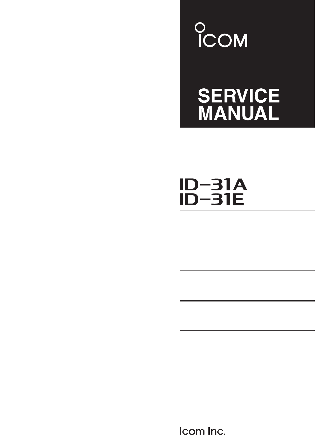
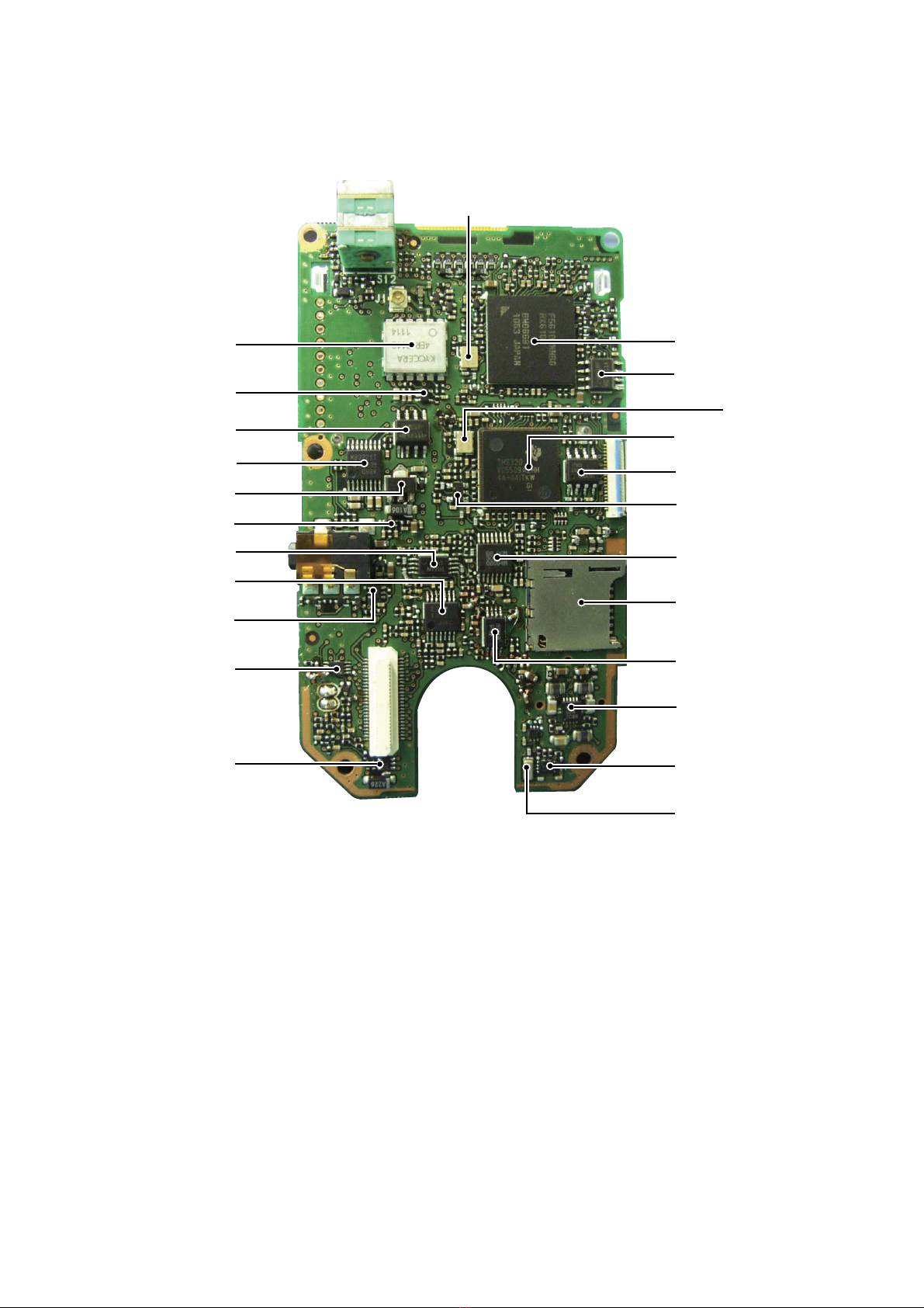
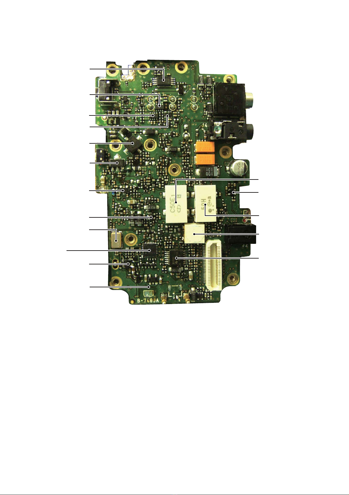
Icom D-STAR ID-31A; D-STAR ID-31E User manual

S-14813XZ-C1
Feb. 2012
UHF TRANSCEIVER

This service manual describes the latest technical
information for the ID-31A/ID-31E UHF TRANSCEIVER, at
the time of publication.
NEVER connect the transceiver to an AC outlet or to a DC
power supply that uses more than the specified voltage.
This will ruin the transceiver.
DO NOT expose the transceiver to rain, snow or any liquids.
DO NOT reverse the polarities of the power supply when
connecting the transceiver.
DO NOT apply an RF signal of more than 20 dBm (100 mW) to
the antenna connector. This could damage the transceiver’s
front-end.
To upgrade quality, any electrical or mechanical parts and
internal circuits are subject to change without notice or
obligation.
MODEL VERSION SUPPLIED
CHARGER
ID-31A
USA BC-167SA
KOR BC-167SD
EXP BC-167SA
EXP-01 BC-167SD
AUS BC-167SV
ID-31E
EUR BC-167SD
UK N/A
ITR BC-167SD
Be sure to include the following four points when ordering
replacement parts:
1. 10-digit Icom part number
2. Component name
3. Equipment model name and unit name
4. Quantity required
<ORDER EXAMPLE>
1110003491 S.IC TA31136FNG ID-31A MAIN UNIT 5 pieces
8820001210 Screw 2438 screw ID-31E Top cover 10 pieces
Addresses are provided on the inside back cover for your
convenience.
ORDERING PARTS
1. Make sure that the problem is internal before dis-
assembling the transceiver.
2. DO NOT open the transceiver until the transceiver is
disconnected from its power source.
3. DO NOT force any of the variable components. Turn them
slowly and smoothly.
4. DO NOT short any circuits or electronic parts. An
insulated tuning tool MUST be used for all adjustments.
5. DO NOT keep power ON for a long time when the
transceiver is defective.
6. DO NOT transmit power into a Standard Signal Generator
or a Sweep Generator.
7. ALWAYS connect a 30–40 dB attenuator between the
transceiver and a Deviation Meter or Spectrum Analyzer,
when using such test equipment.
8. READ the instructions of the test equipment throughly
before connecting it to the transceiver.
REPAIR NOTES
INTRODUCTION
CAUTION
(ID-31A)
Icom, Icom Inc. and the Icom logo are registered trademarks of Icom Incorporated (Japan) in Japan, the United States, the
United Kingdom, Germany, France, Spain, Russia and/or other countries.

TABLE OF CONTENTS
SECTION 1 SPECIFICATIONS
SECTION 2 INSIDE VIEWS
SECTION 3 DISASSEMBLY INSTRUCTION
SECTION 4 CIRCUIT DESCRIPITON
4-1 RECEIVER CIRCUITS. . . . . . . . . . . . . . . . . . . . . . . . . . . . . . . . . . . . . . . . . . . . . . . . . . . . . . . . 4-1
4-2 TRANSMITTER CIRCUITS . . . . . . . . . . . . . . . . . . . . . . . . . . . . . . . . . . . . . . . . . . . . . . . . . . . . 4-2
4-3 FREQUENCY SYNTHESIZER CIRCUITS . . . . . . . . . . . . . . . . . . . . . . . . . . . . . . . . . . . . . . . . 4-3
4-4 VOLTAGE DIAGRAM . . . . . . . . . . . . . . . . . . . . . . . . . . . . . . . . . . . . . . . . . . . . . . . . . . . . . . . . . 4-3
4-5 PORT ALLOCATIONS . . . . . . . . . . . . . . . . . . . . . . . . . . . . . . . . . . . . . . . . . . . . . . . . . . . . . . . . 4-4
SECTION 5 ADJUSTMENT PROCEDURES
5-1 PREPARATION . . . . . . . . . . . . . . . . . . . . . . . . . . . . . . . . . . . . . . . . . . . . . . . . . . . . . . . . . . . . . 5-1
5-2 FREQUENCY ADJUSTMENT . . . . . . . . . . . . . . . . . . . . . . . . . . . . . . . . . . . . . . . . . . . . . . . . . . 5-3
5-3 TRANSMIT ADJUSTMENT . . . . . . . . . . . . . . . . . . . . . . . . . . . . . . . . . . . . . . . . . . . . . . . . . . . . 5-3
5-4 RECEIVE ADJUSTMENT . . . . . . . . . . . . . . . . . . . . . . . . . . . . . . . . . . . . . . . . . . . . . . . . . . . . . 5-7
SECTION 6 PARTS LIST
SECTION 7 MECHANICAL PARTS
SECTION 8 BOARD LAYOUTS
SECTION 9 BLOCK DIAGRAM
SECTION 10 VOLTAGE DIAGRAM

1 - 1
SECTION 1
.
SPECIFICATIONS
DGeneral
• Frequency coverage : (unit: MHz)
Version TX RX
U.S.A. 420–450*1400–479*1
AUS 420–450*2400–479*2
EUR, KOR 430–440 430–440
UK 430–440 400–479*2
ITR 430–434, 435–438 430–434, 435–438
EXP 400–479*2400–479*2
EXP-1 430–440 400–479*2
*
1Guaranteed 440–450 MHz only, *2Guaranteed 430–440 MHz only
• Mode :
FM, FN-N, DV
• No. of memory channels :
552
(incl. 50 scan edges and 2 call channels)
• Usable temp. range : –20°C to +60°C; –4°F to +140°F
• Tuning steps : 5, 6.25, 10, 12.5, 15, 20, 25, 30, 50,
100, 125 and 200 kHz
• Frequency stability : ±2.5 ppm
(–20°C to +60°C; –4°F to +140°F)
• Power supply : 10.0–16.0 V DC for external DC power,
or specified Icom’s battery pack
• Digital transmission speed: 4.8 kbps
• Voice coding speed : 2.4 kbps
• Current drain (at 7.4 V DC) :
TX (at 5 W) Less than 2.5A
RX Max. output FM Less than 350 mA (Internal speaker)
Less than 200 mA (External speaker)
DV Less than 450 mA (Internal speaker)
Less than 300 mA (External speaker)
• Antenna connector : SMA (50 Ω)
• Dimensions : 58(W)×95(H)×25.4(D) mm;
(projections not included) 2.3(W)×3.7(H)×1(D) in
• Weight (approximately) : 140 g; 4.94 oz
(without battery pack/case and ant.)All stated specifications are subject to change without notice or obligation.
DTransmitter
• Modulation system :
FM Variable reactance freq. modulation
DV GMSK reactance freq. modulation
• Output power (at 7.4 V DC) : High 5.0 W, Mid. 2.5 W, Low 0.5 W,
(Typical) S-Low 0.1 W
• Max. frequency deviation : ±5.0 kHz (FM wide: approx.)
±2.5 kHz (FM narrow: approx.)
• Spurious emissions : Less than –60 dBc at High/Mid.
Less than –13 dBm at Low/S-Low
• Ext. mic. impedance : 2.2 kΩ
DReceiver
• Receive system : Double-conversion superheterodyne
• Intermediate frequencies : 46.35 MHz (1st IF)
450 kHz (2nd IF)
• Sensitivity (except spurious points):
FM
(1 kHz/3.5 kHz Dev.; 12 dB SINAD) Less than –15 dBµ
DV (PN9/GMSK 4.8 kbps; BER 1%) Less than –11 dBµ
• Audio output power (at 10% distortion)
Internal speaker : More than 0.4 W with a 16 Ωload
External speaker : More than 0.2 W with a 8 Ωload
• Selectivity :
FM
(Wide) More than 55 dB
FM (Narrow), DV More than 50 dB
• Ext. speaker connector : 3-conductor 3.5(d) mm; (1⁄8˝)/8 Ω
• Spurious and image rejection ratio :
More than 60 dB
• Squelch Sensitivity (threshold, 1 kHz/3.5 kHz Dev.):
Less than –15 dBµ

2 - 1
SECTION 2
.
INSIDE VIEWS
• LOGIC UNIT
(TOP VIEW)
MIC/VOX AMP
(IC19)
RX/TX LED DRIVER
(Q24)
+3.3 V REGULATOR
(IC11)
BACKUP BATTERY
(For the real time clock)
(BT1)

2 - 2
• LOGIC UNIT
(BOTTOM VIEW)
CODEC
(IC15)
SERIAL FLASH MEMORY
(IC20)
EEPROM (For the CPU)
(IC7)
CPU
(IC5)
REAL TIME CLOCK IC
(IC4)
DUAL STEP-DOWN COVERTER
(IC10)
MicroSD CARD SLOT
(J3)
GPS MODULE CONTROLLER
(IC1)
DATA LEVEL CONVERTER
(IC21)
EEPROM (For GPS data)
(IC3)
SERIAL DATA INTERFACE
(IC2)
CPU RESET IC
(IC22)
AF SW
(IC16)
MIC GAIN SW
(Q18)
DSP
(IC18)
CLOCK OSCILLATOR
(For the DSP)
(X3)
CLOCK BUFFER
(For the CODEC)
(IC17)
AF FILTER
(IC13)
CLOCK OSCILLATOR
(For the real time clock IC)
(X1)
AF FILTER
(IC12)
ALC IC
(IC14)
DUAL INVERTER GATE
(IC8)
+3.3 V REGULATOR
(IC9)
CLOCK OSCILLATOR (For the CPU)
(X2)

2 - 3
• MAIN UNIT
(TOP VIEW)
CHARGING LINE SW
(Q7)
DISCRIMINATOR
(X2)
AF FILTER
(IC9)
POWER AMP
(Q45)
VCC LINE SW
(Q8)
DRIVE AMP
(Q41)
YGR
(Q39)
LOCK VOLTAGE BUFFER
(Q26)
D/A CONVERTER
(IC11)
+5 V REGULATOR
(IC15)
+3 V REGULATOR
(IC10)
2ND IF FILTER (For FM mode)
(FI2)
2ND IF FILTER
(For DV/FM-N mode)
(FI1)
REFERENCE FREQUENCY
OSCILLATOR
(X1)
VCC LINE SW
(Q2)
CURRENT DETECTION IC
(IC5)
+5 V REGULATOR
(IC1)

2 - 4
• MAIN UNIT
(BOTTOM VIEW)
STEP-DOWN CONVERTER
(IC4)
+4 V REGULATOR
(IC3)
PLL
(IC6)
BPF TUNING VOLTAGE
BUFFER
(IC12)
RF AMP
(Q47)
1ST IF MIXER
(Q46)
AF POWER AMP
(IC2)
CHARGING LINE DRIVER
(Q6)
IF IC
(IC13)
AF LINE SW
(IC8)
TONE FILTER
(Q31)
AF POWER AMP
REGULATOR
(Q16)
TX POWER SETTING
VOLTAGE BUFFER
(IC14)
1ST IF FILTER
(FI3)

3 - 1
SECTION 3
.
DISASSEMBLY INSTRUCTION
BE CAREFUL about the coaxial cable and connector
when separating the LOGIC UNIT from the chassis.
1. REMOVING THE LOGIC UNIT
1) Remove 2 dials and antenna nut from the front panel.
2) Remove 2 screws from the bottom of chassis.
3) Take out the LOGIC UNIT with chassis from the
front panel.
4) Remove 5 screws from the LOGIC UNIT.
5) Unsolder 6 points at the rotary encoder.
6) Separate the LOGIC UNIT from the chassis, and
then disconnect the coaxial cable from the LOGIC
UNIT.
Inner dial
Outer dial
Antenna nut
Remove with;
“ICOM Driver (Q)”
(8960000370)
Screws
LOGIC UNIT
with chassis
Front panel
UNSOLDER
Solder
remover
Screws x5
LOGIC UNIT
Rotary encoder
J1
LOGIC UNIT
Chassis
Coaxial cable
Suction lifter
Suction lifter
• Part name : EA950R-2
• Manufacture : ESCO CO.LTD
For easy separation of the CHASSIS
Use a suction lifter to lift the bottom of the CHASSIS up.
(Continued on page 3-2)

3 - 2
2. REMOVING THE MAIN UNIT
1) Unsolder 3 points on the shield plate.
UNSOLDER
Solder
remover
Screws x5
MAIN UNIT
Shield plate
UNSOLDER
Solder
remover
Screws x6
Chassis
MAIN UNIT
2) Remove 5 screws from the shield plate, and then
remove it.
3) Unsolder a point at the antenna connector.
4) Remove 6 screws from the MAIN UNIT, and then
remove the MAIN UNIT from the chassis.

4 - 1
• RF CIRCUITS
• 1ST IF CIRCUITS
• 2ND IF CIRCUITS
• RX AF CIRCUITS
• DIGITAL DEMODULATION CIRCUITS
SECTION 4
.
CIRCUIT DESCRIPTION
4-1 RECEIVE CIRCUITS
RF CIRCUITS (MAIN UNIT)
The RX signal from the antenna is passed through two LPFs
(L32, L34, C302, C303, C306, C307, C312 and L29, C281,
C285), ANT SW (D24, D25, D31, D33, L36, C313, C315,
C319) and tuned BPF (D32, L43, C353), and then applied to
the RF AMP (Q47).
The amplified signal is passed through the tuned BPF (D27, D29,
D30, L28, L31, L33, C286, C290, C292, C293, C297, C299–
C301, C304, C305), and then applied to the 1st IF circuits.
1ST IF CIRCUITS (MAIN UNIT)
The RX signal from the RF circuits is applied to the 1st IF
mixer (Q46), and mixed with the 1st LO signal from the VCO
(Q27, D10–D12), resulting in the 46.35 MHz 1st IF signal.
The 1st IF signal is passed through the 1st IF filter (FI3) and
limiter (D23), and then applied to the 1st IF AMP (Q44). The
amplified signal is passed through another limiter (D22), and
then applied to the 2nd IF circuits.
2ND IF CIRCUITS (MAIN UNIT)
The 1st IF signal from the 1st IF circuits is applied to the IF IC
(IC13, pin 16). The IF IC contains the 2nd mixer, 2nd IF AMP,
detector, and so on, in its package.
The 1st IF signal is mixed with the 2nd LO signal from the
reference frequency oscillator (TCXO: X1), resulting in the
450 kHz 2nd IF signal. The 2nd IF signal is passed through
the 2nd IF filter (FI1: for DV/FM-N mode, FI2: for FM mode)
to remove sideband noise. The filtered signal is amplified by
the 2nd IF AMP, and demodulated by the quadrature detector
with discriminator (X2).
The demodulated AF signal is applied to the RX AF circuits.
RX AF CIRCUITS (MAIN AND LOGIC UNITS)
• While operating in the DV mode
The demodulated AF signal is passed through the LPF (MAIN
UNIT: R118, R121, C122, C130, C135), and then applied to
the digital demodulation circuits on the LOGIC UNIT.
The AF signal from the MAIN UNIT is amplified by the AF
AMP (LOGIC UNIT: IC13A, pins 1, 2) and passed through the
LPF (LOGIC UNIT: IC13B, pins 6, 7), and then applied to the
liner CODEC (LOGIC UNIT: IC15, pin 3) to be encoded in to
a digital audio signal.
The digital audio signal is demodulated by the DSP (LOGIC
UNIT: IC18), and then applied to the linear codec (LOGIC
UNIT: IC15) to be decoded into an analog audio signal.
The decoded AF signal is applied to the MAIN UNIT.
The AF signal is passed through the mode SW (MAIN UNIT:
IC8, pins 3, 4) and AF filters (MAIN UNIT: IC9B, pins 6, 7
and IC9C, pins 9, 10), and then applied to the D/A converter
(MAIN UNIT: IC11, pin 13) to be adjusted in level.
• While operating in the FM/FM-N mode
The demodulated AF signal is passed through the LPF (R272,
C355), mode SW (MAIN UNIT: IC8, pins 1, 2) and AF filters
(MAIN UNIT: IC9B, pins 6, 7 and IC9C, pins 9, 10), and then
applied to the D/A converter (MAIN UNIT: IC11, pin 13) to be
adjusted in level.
The level-adjusted AF signal is amplified by the AF power
AMP (MAIN UNIT: IC2, pin 1), and then output from the in-
ternal speaker (CHASSIS: SP1) or external speaker, through
the SP jack (MAIN UNIT: J4).
RF
LPF LPF
BPF BPF
ANT
SW
D27,D29,D30
To the 1st IF circuits
From the TX AMP circuits
D32
D24,D25
D31,D33
IF
AMP
LPF
BPF
XTAL
46.35MHz
FI3D23D22
To the 2nd IF circuits
To the RF circuits
From the VCO
LIMIT
Q46
Q44
1st LO
LIMIT
BPF
CERAMIC
BPF
CERAMIC
BPF
Q38
X1
X2
From the 1st IF circuits
To the RX AF circuits DISCRI
IC13
IF IC
FI2
15.3MHz
W/N
SW
FI1
Q36,D15
To the digital
demodulation circuits.
X3
REF
45.9MHz
FM
FM-N/DV
D16,D18,D19
LPF
LPF DAFO
DDET
To the RX AF circuits
Q31
CODEC
LINEAR
DSP
IC15
IC13B
IC18
IC13A
RTONE
AMP From the 2nd IF circuits
AF
AMP
J4
SP1
LPF
IC2
VO-
VO+
From the 2nd IF circuits
D/A
IC11
FILTER SW
MODE
AF
IC9B,C
Q23
IC8
From the digital
demodulation circuits.
IC16
AFON
CHASSIS UNIT
[SP]

4 - 2
4-2 TRANSMIT CIRCUITS
TX AF CIRCUITS (LOGIC AND MAIN UNITS)
The AF signal from the internal or external microphone (MIC
signal) is applied to the MIC AMP (LOGIC UNIT: IC19B, pin 5).
• When operating in the DV mode
The amplified signal is passed through the MIC mute SW
(LOGIC UNIT: IC16, pins 1, 7), and then further amplified by
the ALC AMP (LOGIC UNIT: IC14, pin 1). The amplified sig-
nal is applied to the liner CODEC (LOGIC UNIT: IC15, pin 2),
through the buffer (LOGIC UNIT: IC12B, pins 6, 7), to be en-
coded into a digital audio signal.
The digital audio signal is processed by the DSP (LOGIC
UNIT: IC18), and then applied to the linear codec (LOGIC
UNIT: IC15) to be converted into the digital baseband signal.
The digital baseband signal is passed through the LPF (LOGIC
UNIT: IC12A, pins1, 3), and then applied to the MAIN UNIT.
The digital baseband signal is passed through the mode SW
(MAIN UNIT: IC8, pins 10, 11), and then applied to the D/A
converter (MAIN UNIT: IC11, pin 18) to be adjusted in level.
TX AMP CIRCUITS (MAIN UNIT)
The TX signal is passed through the buffer (Q48) and
attenuator (D20, D21) which controls the TX output power by
the APC AMP (IC14). The TX signal is sequentially amplified
by the YGR (Q39) and drive AMP (Q41), and then passed
through the LPF (L42, C250, C351). The filtered TX signal is
applied to the power AMP (Q45).
The amplified TX signal is passed through the LPF (L22, L24,
C260, C265, C267, C270), ANT SW (D24, D25), TX output
power detector (D26, D28) and two LPFs (L29, C281, C285
and L32, L34, C302, C303, C306, C307, C312), before being
applied to the antenna.
APC CIRCUITS (MAIN UNIT)
The voltage produced at the LPFs (L29, C281, C285 and
L32, L34, C302, C303, C306, C307, C312) is rectified by D26
and D28, and it is used as the TX power sensing voltage.
The voltage is applied to the APC AMP (IC14, pin 7), and the
output voltage controls the bias voltages of attenuator (D20,
D21) to keep the TX output power constant.
MODULATION CIRCUITS (MAIN UNIT)
The MIC signal from the TX AF circuits is applied to the VCO
(Q27, D10–D12) as a modulation signal. The modulation sig-
nal is applied to D10 to obtain GMSK (For DV mode) or Fre-
quency Modulation (For FM mode).
The modulated VCO output signal is passed through the buf-
fer (Q30) and amplified by the LO AMP (Q32), and then ap-
plied to the TX AMP circuits as the TX signal, through the LO
SW (D14).
HPF
J5
MIC
AMP
MC1 BPF LPF
LPF
BUFF
ALC
AMP
VCOMOD
To the modulation circuits
IC9A
D/A
IC9D
MOD
SW
GAIN
Q18
CODEC
LINEAR
DSP
IC15
SW
MODE
IC19B
DMI DMO
MMUTE
SW
IC16
IC14 IC12B
IC18
IC11
MAIN UNIT
LOGIC UNIT
IC8,Q22
IC12A
DMOD
EXTMIC
MAIN UNIT
FM
FM mode DV
DV mode
VCO BUFF LO
AMP
To the TX AMP circuits
From the TX AF circuits
D13,D14
SW
Q27,
D10,D11,D12
LO
Q32
Q30
APC
CTRL
PWR
AMP LPF
PWR
DET
LPFATT YGR
AMP LPF
DRV.
AMP ANT
SW
BUFF
D20,D21
From
the VCO
Q39 Q41 Q45 D26,D28
RX circuits
IC14B
D24,D25
Q48
D31,D33
• When operating in the FM/FM-N mode
The amplified signal is passed through the MIC mute SW
(LOGIC UNIT: IC16, pins 1, 7), and then applied to the MAIN
UNIT.
The MIC signal is passed through the HPF (MAIN UNIT: R78,
C77, C80), BPF (MAIN UNIT: IC9A, pins 1, 3), LPF (MAIN
UNIT: IC9D, pins 13, 14) and mode SW (MAIN UNIT: IC8,
pins 8, 9), and then applied to the D/A converter (MAIN UNIT:
IC11, pin 18) to be adjusted in level.
The level-adjusted signal is applied to the modulation cir-
cuits.
• TX AF CIRCUITS
• MODULATION CIRCUITS
• TX AMP AND APC CIRCUITS

4 - 3
• FREQUENCY SYNTHESIZER CIRCUITS
4-4 VOLTAGE DIAGRAM
Voltage from the power supply is routed throughout the transceiver, through regulators and switches.
4-3 FREQUENCY SYNTHESIZER (MAIN UNIT)
• VCO
The ID-31A/E has a VCO (Q27, D10–D12) which generates
both the 1st LO signal and the TX signal. The output of buffer
(Q30) is amplified by the LO AMP (Q32), and then used as
the TX/RX LO signal.
While receiving, the LO signal is applied to the 1st IF mix-
er (Q46), through the LO SW (D13) and LPF (L30, C280,
C289).
While transmitting, the LO signal is applied to the TX AMP cir-
cuits, through the LO SW (D14), buffer (Q48) and attenuator
(D20, D21).
LPF
FILTER
LOOP VCO
LPF
BUFF
PLL
IC
BUFF
LO
AMP
BPF
Q38
FIN D13,D14
X1
Q29
IC13
DET
SW
FM
Q27,D10,D11,D12
LO
15.3MHz
Q46
IC6
Q32
Q30
1st LO
1st IF mixer
TX AMPs
X3
REF
45.9MHz
J2
CHG
IC4
IC5,D9
VCC
TXI-V
HV
CURRENT
S
-
SW
+
R3C
CTRL
T3C_INV
DC
CHGC
PCON
REG
Q15,Q16
VCC
Q24
RX circuits Common circuits Common circuits
TX circuits AF power AMP
VCO, reference
frequency oscillator,etc.
CHG
BTVIN
Q6,Q7,Q9,Q10
VCC-I
R3 DETECT
T3C
R3
SW
REG
REG
Q37,D17
T5
T3C_INV
YGR
REG
IC10
3VS
REG
SP
BTL5V
3VS
3VS
BTDET
IC1,
Q1,Q2,Q3,Q8,
D1,D3,D4
D2,D5,D6
CHGH
PS3
+5V
+5V
REG
5VS
IC15
Q17,Q19
• PLL
A portion of VCO output signal is passed through two buffers
(Q29 and Q30) and LPF (L7, C137–C139, C144), and then
fed back to the PLL IC (IC6, pin 8).
The PLL IC (IC6) phase-compares the output of reference
frequency oscillator (TCXO; X1) and VCO, and the phase-
difference is output as the charge pump current. The current
is passed though the loop filter (R67, R71, R90, R93, C74,
C91, C92, C96, C102) to be converted into the lock voltage,
which controls the oscillating frequency of VCO.
When the oscillation frequency drifts, its phase changes from
that of the reference frequency, causing a lock voltage change
to compensate for the drift in the VCO oscillating frequency.

4 - 4
BALL
No.
LINE
NAME DESCRIPTION I/O
A4 G_RES
GPS module (CHASSIS: EP1) controller
(IC1) reset.
L: Reset.
O
A5 REMOTE HM-75A key input detect. I
A6 VIN External power supply voltage. I
A7 RTONE DV signal/recorded audio. I
A8 TTEMP TX AMP (MAIN UNIT: Q45) temperature
sensing voltage. I
A10 DICK1 [DIAL] (outer dial) (S12) phase-A I
A11 UNLK PLL unlock detect.
L: Unlock is detected. I
A12 DALD D/A converter (MAIN UNIT: IC11) strobe.
(“H” and “L” are reversed.) O
A13,
A14
KS0,
KS2 Key matrix ports. O
B1 DTMF DTMF/European tone/Beep signal. O
B5 LV Lock voltage. I
B7 TXI-V TX current flow sensing voltage. I
B8 TEMP Temperature sensing voltage. I
B10 DIUD1 [DIAL] (outer dial) (S12) phase-B I
B11 CLSFT CPU clock frequency control.
H: The clock frequency is shifted. O
B13 KS1 Key matrix port. O
B15 KR0 Key input detect. I
C2 CTCSS CTCSS/DTCS tone signal. O
C5 VOX VOX sensing voltage. I
C7 CTCIN CTCSS tone signal input. I
C10 DIUD2 [DIAL] (inner dial) (S12) phase-B. I
C11 DTCS
CTCSS/DTCS filter (R65, R68, C78, C80)
switching.
H: DTCS is in use.
O
C13 KS3 Key matrix port. O
C14 KR1 Key input detect. I
C15 DCIN External power supply connection detect.
L: External DC input. I
D1 DADATA D/A converter serial data.
(“H” and “L” are reversed.) O
D2 G_RXD GPS data input. I
D4 DCSFT DSP clock frequency control.
L: Clock frequency is shifted. O
D5 BTSENC
Battery type detect.
(Detecting intermediate voltage of the bat-
tery pack.)
I
D6 BTVIN Battery pack voltage. I
D7 RSSI S-meter voltage. I
D10 DICK2 [DIAL] (inner dial) (S12) phase-A. I
D11 DACK D/A converter (MAIN UNIT: IC11) clock.
(“H” and “L” are reversed.) O
D12 KR2 Key input detect. I
D13 BTDET Battery attachment detect.
L: Battery attached. I
D14 PWRSW [POWER] key.
L: Pushed. I
E4 G_TXD GPS data output. O
F12 CHGC Charging ON/OFF control.
H: While charging. O
F13 TXLED TX LED (DS7) driver (Q9) control.
H: While transmitting. O
F15 BLED BUSY LED (DS7) driver (Q8) control.
H: While the squelch is open. O
G1 RESET CPU reset.
L: Reset. I
BALL
No.
LINE
NAME DESCRIPTION I/O
G3 LIGHT LCD and key backlight (DS1, DS3) driver
(Q23) control. O
G4 DIM LCD backlight (DS1, DS3) dimmer control.
H: Blight. O
G12 INTMIC Internal MIC (MAIN UNIT: MC1) control.
H: Internal microphone is in use. O
G14 CHGH Charging current control.
H: While charging. O
G15 PCON
Power lines “PS3” and “5VS” SW (MAIN
UNIT: IC4) control.
H: While the transceiver’s power is ON.
O
H12 VCO_
SEL
VCO power supply control.
L: While the transceiver's power is ON. O
J4 RTC_
IRQ Real time clock “IRQ” input. I
J12 MMUTE MIC mute SW (IC16) control.
L: Mute. O
J13 TXMUTE TX mute SW (MAIN UNIT: Q43) control.
H: mute. O
J15 PFMC GPS/DSP operating mode control. O
K1 NOIS Noise level sensing voltage. I
K4 DSP_
REQ DSP “REQ” input. I
K12 VCO_
MUTE
Modulation mute SW (MAIN UNIT: Q21)
control.
H: Mute.
O
K13 WN
2nd IF filter (MAIN UNIT: FI1 and FI2)
switching control.
L: FI1 is selected. (While in the FM-N or
DV mode.)
O
K14 MIC1
MIC gain control.
MIC1 MIC2 MIC gain
level
LL 4
HL 3
LH 2
HH 1
O
K15 MIC2
L12 SQL [SQL] (MAIN UNIT: S1) input.
L: Pushed. I
L14 PS3C Power line “PS3C” SW (Q13) control.
L: While in the power save mode. O
L15 R3C
Power line “R3C” SW (MAIN UNIT: Q24)
control.
L: While receiving.
O
M2 CLOUT Cloning data. O
M5 DSP_
STB DSP (IC18) strobe. O
M6 DSPC
Power line “CVDD_1.35V” SW (IC10) control.
H: While the DSP’s power is ON. O
M7 PPS PLL operating mode control.
H: While in the power save mode. O
M8 LCDRS LCD (DS10) reset. O
M9 LCDCS LCD (DS10) chip select. O
M10 DSP_
REMP DSP “REC EMP” input. I
M12 TX232 RS-232C serial data output. O
M14 ESIO EEPROM (IC7) serial data. I/O
M15 T3C
Power line “T3C” SW (MAIN UNIT: Q17,
Q19) control.
H: While transmitting.
O
N1 CLIN Cloning data. I
N2 SD_
SENC
SD Card insertion detect.
L: A microSD card is inserted. I
N3 SD_TXD MicroSD card data output. O
4-5 PORT ALLOCATIONS
• CPU (LOGIC UNIT: IC5)

4 - 5
• D/A CONVERTER (MAIN UNIT: IC11)
BALL
No.
LINE
NAME DESCRIPTION I/O
N4 DSP_SI DSP (IC10) serial data. I
N5 DSP_
AFC1 DSP (IC10) “AFC” input. I
N6 RTC_
SDA Serial data to the real time clock (IC4). I/O
N7 PLLSTB PLL IC (MAIN UNIT: IC6) strobe. O
N9 LCDDT LCD (DS10) serial data. O
N10 DSP_
DEMP DSP (IC18) “DATA EMP” input. I
N12 G_HIB
GPS module (CHASSIS: EP1) controller
(IC1) power control.
H: GPS module is ON.
O
N15 ECK EEPROM (IC7) clock. O
P1 SD_CS MicroSD card chip select. O
P2 SD_SCK MicroSD card clock output. O
P4 DSP_CK DSP (IC18) clock. O
P5 DSP_PD DSP (IC18) operating mode control.
H: While in the power save mode. O
P6 LCDRES LCD (DS10) reset. O
P7 PLLDATA PLL IC (MAIN UNIT: IC6) serial data. O
P9 PLL SW PLL lockup time control.
L: Fast lockup time. O
P12 GPSC
GPS module (CHASSIS: EP1) controller
(IC1) switching.
H: GPS module’s power is ON.
O
P13 RX232 RS-232C serial data input. I
P14 INTPTT Internal PTT (MAIN UNIT: S2) input.
L: Pushed. I
R1 SD_RXD MicroSD card card data input. I
R2 DSP_SO DSP (CI18) serial data. O
R4 DSP_
AFC2 DSP (IC18) “AFC” input. I
R5 DSP_
RESET
DSP (IC18) reset.
H: Reset. O
R6 RTC_
SCL
Clock signal to the real time clock IC
(IC4). O
R7 PLLCK PLL IC (MAIN UNIT: IC6) clock. O
R8 LCDCK LCD (DS10) clock. O
R13 AFON AF power AMP (MAIN UNIT: IC2) control.
L: AF power AMP activated. O
R14 EXTPTT External PTT input. I
• CPU (LOGIC UNIT: IC5) (Continued)
PIN
No.
LINE
NAME DESCRIPTION I/O
7 BPF1 Tuning voltage to the BPF (D32, L40,
C353). O
8 BPF3
Tuning voltage to the BPF (D27, D29, D30,
L28, L31, L33, C286, C290, C292, C293,
C297, C299–C301, C304, C305).
O
11 SQLOUT Noise squelch level adjustment. O
12 RXAFOUT RX AF output level adjustment. O
19 VCOMOD VCO (Q27, D10–D12) deviation adjust-
ment. O
20 REFMOD Reference oscillator (X1) deviation adjust-
ment. O
24 BPF2
Tuning voltage to the BPF (D27, D29, D30,
L28, L31, L33, C286, C290, C292, C293,
C297, C299–C301, C304, C305).
O

5 - 1
SECTION 5
.
ADJUSTMENT PROCEDURE
¤ CONNECTION
¤ JIG CABLES
EQUIPMENT GRADE AND RANGE EQUIPMENT GRADE AND RANGE
Power supply Voltage range : 1–15 V
Current capacity : More than 3 A JIG cable Modified 3-conductor plugs
(See the illustration below)
Audio generator
(AG)
Frequency range : 300–3000 Hz
Output level : 1–500 mV Attenuator Power attenuation : 40 dB
Capacity : More than 6 W
Modulation
Analyzer
Frequency range : 30–600 MHz
Measuring range : 0 to ±10 kHz
Standard signal
generator (SSG)
Frequency range : 0.1–600 MHz
Output level : –20 dBµ to 90 dBµ
(–127 to –17 dBm)
AC millivoltmeter Measuring range : 10 mV to 10 V
Frequency counter
Frequency range : 0.1–600 MHz
Frequency accuracy : ±1 ppm or better
Input level : Less than 1 mW
RF power meter
(50 Ω terminated)
Measuring range : 0.1–6 W
Frequency range : 100–600 MHz
SWR : Less than 1.2 : 1
¤ REQUIRED EQUIPMENTS
5-1 PREPARATION
To the [DC IN] jack
OPC-254L
:
e
t
i
h
W
:kc
a
lB
DC power supply
13.5 V/3 A
FM
deviation meter
to the antenna connector
Attenuator
40 dB
RF power meter
0.1–6 W/50 Ω
Frequency
counter
Standard signal generator
–20 to 90 dBµ
(–127 dBm to –17 dBm)
DO NOT transmit while
an SSG is connected to
the antenna connector.
• Adjustment at 5.5 V or 7.4 V
Be sure about the polarity
DC power supply
5.5 V or 7.4 V/3 A
• Adjustment at 13.5 V
POWER SUPPLY CONNECTION
To [SP]
[DC IN]
To [MIC]
JIG cables
SETTING;
Frequency : 1 kHz
Level : 90 mVrms
Waveform : Sine wave
3-conductor 2.5 (d) mm
• JIG cable #1
• JIG cable #2
plug
(EXTMIC)
(GND)
33 k
+−
AC
MILLIVOLTMETER
(10 mV to 10 V)
AUDIO GENERATOR
(300–3000 Hz/1–500 mV)
+−
PTT
+
4.7 µF
3-conductor 3.5 (d) mm plug
(CLONE)
(SP)
(GND)
82 kΩ
Less than 4.5 (d) mm

5 - 2
• ENTERING THE ADJUSTMENT MODE
1) Connect the JIG cable “#1” (See page 5-1) to [SP].
2) While holding down [SQL] and , turn ON the power.
• KEY ASSIGNMENTS FOR THE ADJUSTMENT MODE
• QUITING THE ADJUSTMENT MODE
1) Remove the JIG cable “#1” from [SP].
2) Turn OFF the power, and then turn ON the power.
Adjustment frequency
Adjustment item Adjustment value
Adjusts the value for the item
Selects the previous adjustment item
Selects the next adjustment item
(without storing value) Stores the value for the item
TX output power
Mode
Push to turn ON the power.
[SQL]
[QUICK/MENU]
Connect the JIG cable “#1” (See page 5-1) here.

5 - 3
5-2 FREQUENCY ADJUSTMENT
Select an adjustment item using /, and then set the adjustment value as specified using [DIAL].
ADJUSTMENT
ADJUSTMENT
ITEM
OPERATION VALUE
REFERENCE
FREQUENCY
[REF]
1 1) Set the power supply voltage to 7.4 V.
2) Connect a power meter or dummy load to the antenna connec-
tor.
3) Loosely couple a frequency counter to the antenna connector.
4) While transmitting, adjust the frequency using [DIAL], and then
push [ENT] to store the adjustment value.
Displayed
frequecny
(±200 Hz)
5-3 TRANSMIT ADJUSTMENT
• IDLING CURRENT ADJUSTMENT (at 5.5 V)
Select an adjustment item using /, and then set the adjustment value as specified using [DIAL].
ADJUSTMENT
ADJUSTMENT
ITEM OPERATION VALUE
DRIVE AMP
IDLING CURRENT
[ID5]
1 1) Set the power supply voltage to 5.5 V.
2) Connect an RF power meter to the antenna connector.
3) Connect a ammeter between the power supply and transceiver.
4) Set the item [IP5] to "00."
–
2•While transmitting, adjust the idling current using [DIAL], and then
push [ENT] to store the adjustment value. 120–140 mA
FINAL AMP
IDLING CURRENT
[IP5]
1 1) Set the power supply voltage to 5.5 V.
2) Connect an RF power meter to the antenna connector.
3) Connect a ammeter between the power supply and transceiver.
–
2•While transmitting, adjust the idling current using [DIAL], and then
push [ENT] to store the adjustment value. 180–280 mA
• IDLING CURRENT ADJUSTMENT (at 7.4 V)
Select an adjustment item using /, and then set the adjustment value as specified using [DIAL].
ADJUSTMENT
ADJUSTMENT
ITEM OPERATION VALUE
DRIVE AMP
IDLING CURRENT
[ID7]
1 1) Set the power supply voltage to 7.4 V.
2) Connect an RF power meter to the antenna connector.
3) Connect a ammeter between the power supply and transceiver.
4) Set the item [IP7] to "00."
–
(Hi power) 2•While transmitting, adjust the idling current using [DIAL], and then
push [ENT] to store the adjustment value.
170–190 mA
(Mid power) 3120–140 mA
(Low power) 4
100–120 mA
(S-Low power) 5
FINAL AMP
IDLING CURRENT
[IP7]
1 1) Set the power supply voltage to 7.4 V.
2) Connect an RF power meter to the antenna connector.
3) Connect a ammeter between the power supply and transceiver.
–
(Hi power) 2•While transmitting, adjust the idling current using [DIAL], and then
push [ENT] to store the adjustment value.
880–980 mA
(Mid power) 3 480–580 mA
(Low power) 4160–260 mA
(S-Low power) 5
NOTE: When "IDLING CURRENT" is adjusted, "TRANSMIT POWER" must be alos re-adjusted.

5 - 4
• IDLING CURRENT ADJUSTMENT (at 13.5 V)
Select an adjustment item using /, and then set the adjustment value as specified using [DIAL].
ADJUSTMENT
ADJUSTMENT
ITEM
OPERATION VALUE
DRIVE AMP
IDLING CURRENT
[ID1]
1 1) Set the power supply voltage to 13.5 V. (supplying from [DC IN])
2) Connect an RF power meter to the antenna connector.
3) Connect a ammeter between the power supply and transceiver.
4) Set the item [IP1] to "00."
–
(Hi power) 2•While transmitting, adjust the idling current using [DIAL], and then
push [ENT] to store the adjustment value.
100–120 mA
(Mid power) 3 90–110 mA
(Low power) 480–100 mA
(S-Low power) 5
FINAL AMP
IDLING CURRENT
[IP1]
1 1) Set the power supply voltage to 13.5 V. (supplying from [DC IN])
2) Connect an RF power meter to the antenna connector.
3) Connect a ammeter between the power supply and transceiver.
–
(Hi power) 2•While transmitting, adjust the idling current using [DIAL], and then
push [ENT] to store the adjustment value.
550–670 mA
(Mid power) 3 350–450 mA
(Low power) 4140–240 mA
(S-Low power) 5
NOTE: When "IDLING CURRENT" is adjusted, "TRANSMIT POWER" must be also re-adjusted.
• TRANSMIT POWER ADJUSTMENT (at 5.5 V)
Select an adjustment item using /, and then set the adjustment value as specified using [DIAL].
ADJUSTMENT
ADJUSTMENT
ITEM
OPERATION VALUE
TRANSMIT
POWER
[PO5]
1 1) Set the power supply voltage to 5.5 V.
2) Connect an RF power meter to the antenna connector.
3) While transmitting, adjust the TX power using [DIAL], and then
push [ENT] to store the adjustment value.
80–120 mW
(BAND LOW) 2
(BAND HIGH) 3
NOTE: When "IDLING CURRENT" is adjusted, "TRANSMIT POWER" must be also re-adjusted.
• TRANSMIT POWER ADJUSTMENT (at 7.4 V)
Select an adjustment item using /, and then set the adjustment value as specified using [DIAL].
ADJUSTMENT
ADJUSTMENT
ITEM
OPERATION VALUE
TRANSMIT POWER
[PO7]
1 1) Set the power supply voltage to 7.4 V.
2) Connect an RF power meter to the antenna connector. –
(Hi power)
[BAND LOW]
2•While transmitting, adjust the TX power using [DIAL], and then
push [ENT] to store the adjustment value. 4.8–5.2 W
[BAND HIGH]
(Mid power)
[BAND LOW]
3
2.3–2.7 W
[BAND HIGH]
(Low power)
[BAND LOW]
4
0.4–0.6 W
[BAND HIGH]
(S-Low power)
[BAND LOW]
5
80–120 mW
[BAND HIGH]
5-3 TRANSMIT ADJUSTMENT (Continued)

5 - 5
• TRANSMIT POWER ADJUSTMENT (at 13.5 V)
Select an adjustment item using /, and then set the adjustment value as specified using [DIAL].
ADJUSTMENT
ADJUSTMENT
ITEM
OPERATION VALUE
TRANSMIT POWER –1 1) Set the power supply voltage to 13.5 V. (supplying from [DC IN])
2) Connect an RF power meter to the antenna connector. –
(Hi power)
[BAND LOW]
[PO1]
2•While transmitting, adjust the TX power using [DIAL], and then
push [ENT] to store the adjustment value. 4.8–5.2 W
[BAND HIGH] 3
(Mid power)
[BAND LOW]
4
2.3–2.7 W
[BAND HIGH] 5
(Low power)
[BAND LOW]
6
0.4–0.6 W
[BAND HIGH] 7
(S-Low power)
[BAND LOW]
8
80–120 mW
[BAND HIGH] 9
• DEVIATION ADJUSTMENTS
Select an adjustment item using /, and then set the adjustment value as specified using [DIAL].
ADJUSTMENT
ADJUSTMENT
ITEM
OPERATION VALUE
FM DEVIATION
–
1 1) Set the power supply voltage to 7.4 V.
2) Connect a modulation analyzer to the antenna connector through
an attenuator, and set it as;
HPF : OFF
LPF : 20 kHz
De-emphasis : OFF
Detector : (P-P)/2
3) Connect an audio generator to the JIG cable (See page 5-1).
–
[FM (BAND LOW)] [MFL] 2 1) Set the audio generator as;
Frequency : 1 kHz
Level : 90 mVrms
2) While transmitting, adjust the deviation using [DIAL], and then
push [ENT] to store the adjustment value.
±4.1 to ±4.3 kHz
[FM-N (BAND HIGH)] [MNL] 3 ±2.0 to ±2.2 kHz
[FM (BAND LOW)] [MFH] 4 ±4.1 to ±4.3 kHz
[FM-N (BAND HIGH)] [MNH] 5 ±2.0 to ±2.2 kHz
REF DEVIATION
[FM (BAND LOW)] [BFL] 1 1) Set the audio generator as;
Level : 0 mVrms (OFF)
2) While transmitting, adjust the deviation using [DIAL], and then
push [ENT] to store the adjustment value.
Minimum
deviation
[FM-N (BAND HIGH)] [BNL] 2
[FM (BAND LOW)] [BFH] 3
[FM-N (BAND HIGH)] [BNH] 4
DV DEVIATION
–
1 1) Set the power supply voltage to 7.4 V.
2) Connect a modulation analyzer to the antenna connector through
an attenuator, and then set it as;
HPF : OFF
LPF : 20 kHz
De-emphasis : OFF
Detector : (P-P)/2
3) No audio signal is applied.
–
[BAND LOW]
[DVV]
2•While transmitting, adjust the deviation using [DIAL], and then
push [ENT] to store the adjustment value. ±0.95 to ±1.15
kHz
[BAND CENTER] 3
[BAND HIGH] 4
DV BALANCE
–
1 1) Set the power supply voltage to 7.4 V.
2) Connect a modulation analyzer to the antenna connector through
an attenuator, and then set it as;
HPF : OFF
LPF : 20 kHz
De-emphasis : OFF
Detector : (P-P)/2
3) No audio signal is applied.
–
[BAND LOW]
[DVR]
2•While transmitting, adjust the deviation using [DIAL], and then
push [ENT] to store the adjustment value. Minimum
deviation
[BAND CENTER] 3
[BAND HIGH] 4
5-3 TRANSMIT ADJUSTMENT (Continued)
Other manuals for D-STAR ID-31A; D-STAR ID-31E
3
This manual suits for next models
1
Table of contents
Other Icom Transceiver manuals