IDT 82V3911 User manual

EVALUATION BOARD USER’S GUIDE
WAN PLL 82V3911
82V3911 REVISION 1 1/30/15 1©2014 Integrated Device Technology, Inc.
INTRODUCTION
The 82V3911 evaluation board kit, including an evaluation board and
evaluation software, provides a platform to evaluate 82V3911.
The evaluation board kit contains the following components:
• 82V3911 evaluation board ver 1.00 with all necessary components
• 82V3911 evaluation GUI software ver 1.00
• 82V3911 evaluation board user’s guide ver 1.0
FEATURES
• Professional evaluation software to configure and monitor the device
• Current configuration data can be saved as a file for later use
PC REQUIREMENTS
The 82V3911 evaluation software runs on Microsoft Windows. The
system requirements are as follows:
• Pentium 166 MMX or higher (recommended)
• Minimum 500M bytes free hard disk space
• Minimum 64M bytes memory
• Display with the resolution of 1024x768, small font (recommended)
• Operating System: Microsoft Windows 2000/XP/NT (English version
recommended) or newer OS version
• Microsoft Windows compatible 2-button or 3-button mouse

82V3911 WAN PLL
EVALUATION BOARD USER’S GUIDE 2REVISION 1 1/30/15
INTRODUCTION...................................................................................................................................................................... 1
FEATURES.............................................................................................................................................................................. 1
PC REQUIREMENTS............................................................................................................................................................... 1
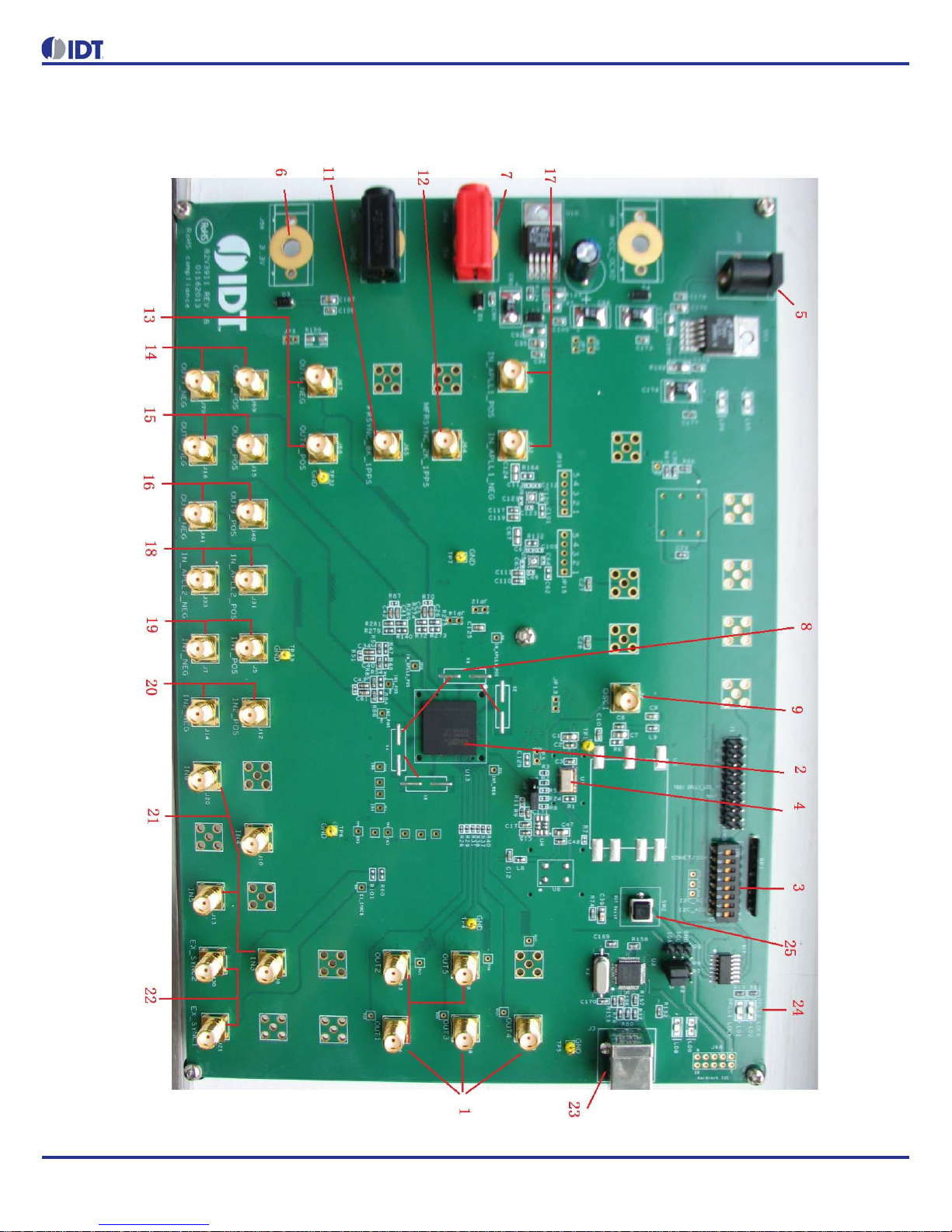
1 HARDWARE CONFIGURATION ....................................................................................................................................3
1.1 ANNOTATION FOR FIGURE-1 ..........................................................................................................................4
2 SOFTWARE CONFIGURATION .....................................................................................................................................5
2.1 INSTALLATION ..................................................................................................................................................5
2.2 GENERAL INTRODUCTION ..............................................................................................................................5
2.2.1 Overview.................................................................................................................................................5
2.2.2 Conventions used...................................................................................................................................5
2.2.3 DPLL1/ DPLL2 Path Selection...............................................................................................................6
2.2.4 Read/Write the Configuration Data.........................................................................................................6
2.2.5 Load/Save the Configuration Data.........................................................................................................6
2.2.6 Tips for the Parameters and Buttons......................................................................................................7
2.2.7 Menu Bar................................................................................................................................................7
2.2.8 Shortcut Icons.........................................................................................................................................8
2.2.9 Status Bar...............................................................................................................................................8
2.3 INITIALIZATION .................................................................................................................................................9
2.4 INPUT PORTS STATUS AND CONFIGURATION .............................................................................................9
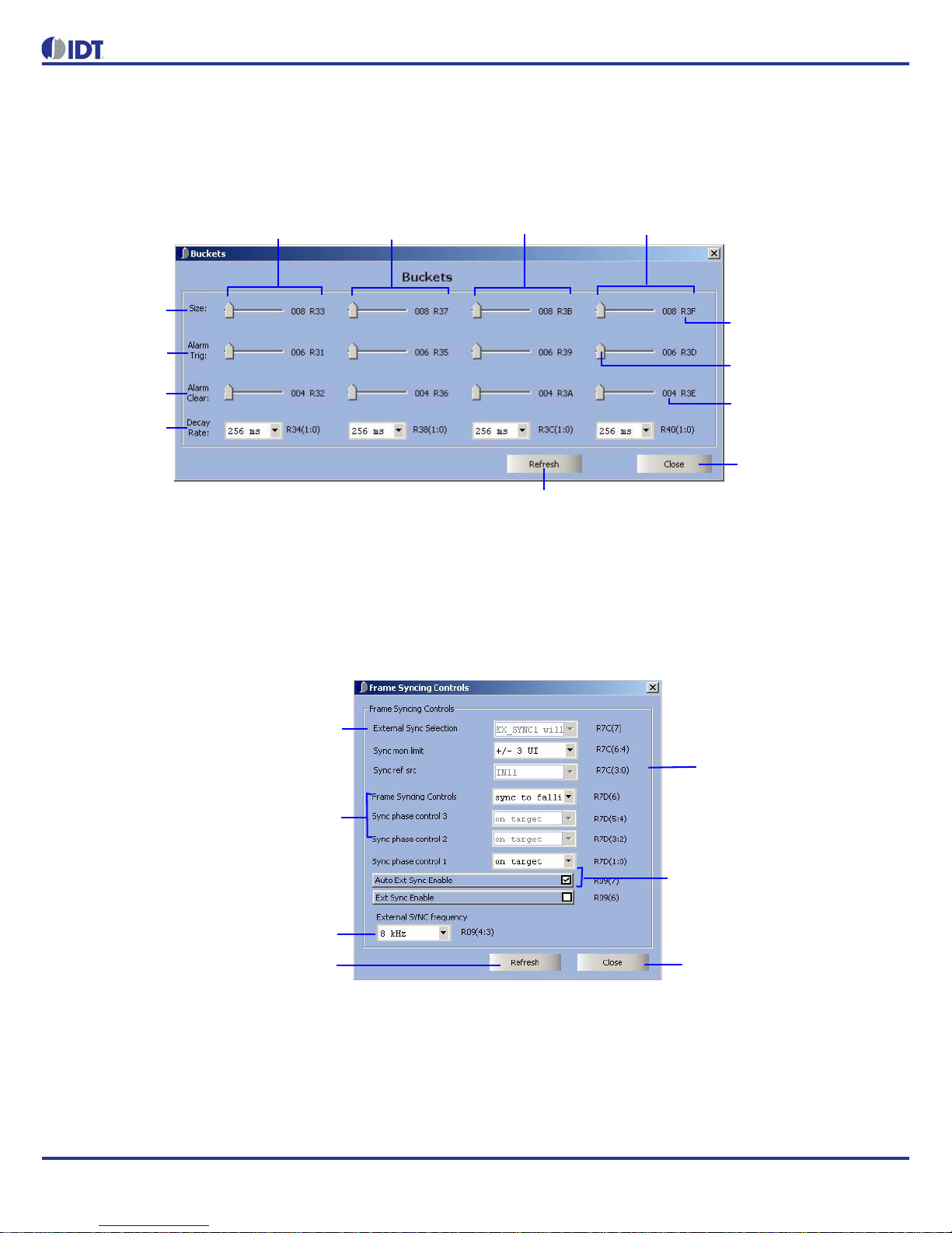
2.4.1 Leaky Bucket Configuration..................................................................................................................11
2.4.2 Frame Synchronization Control............................................................................................................11
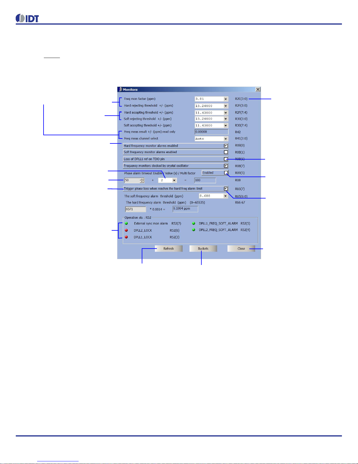
2.5 MONITOR CONFIGURATION ..........................................................................................................................12
2.6 DPLL2 PATH CONFIGURATION .....................................................................................................................13
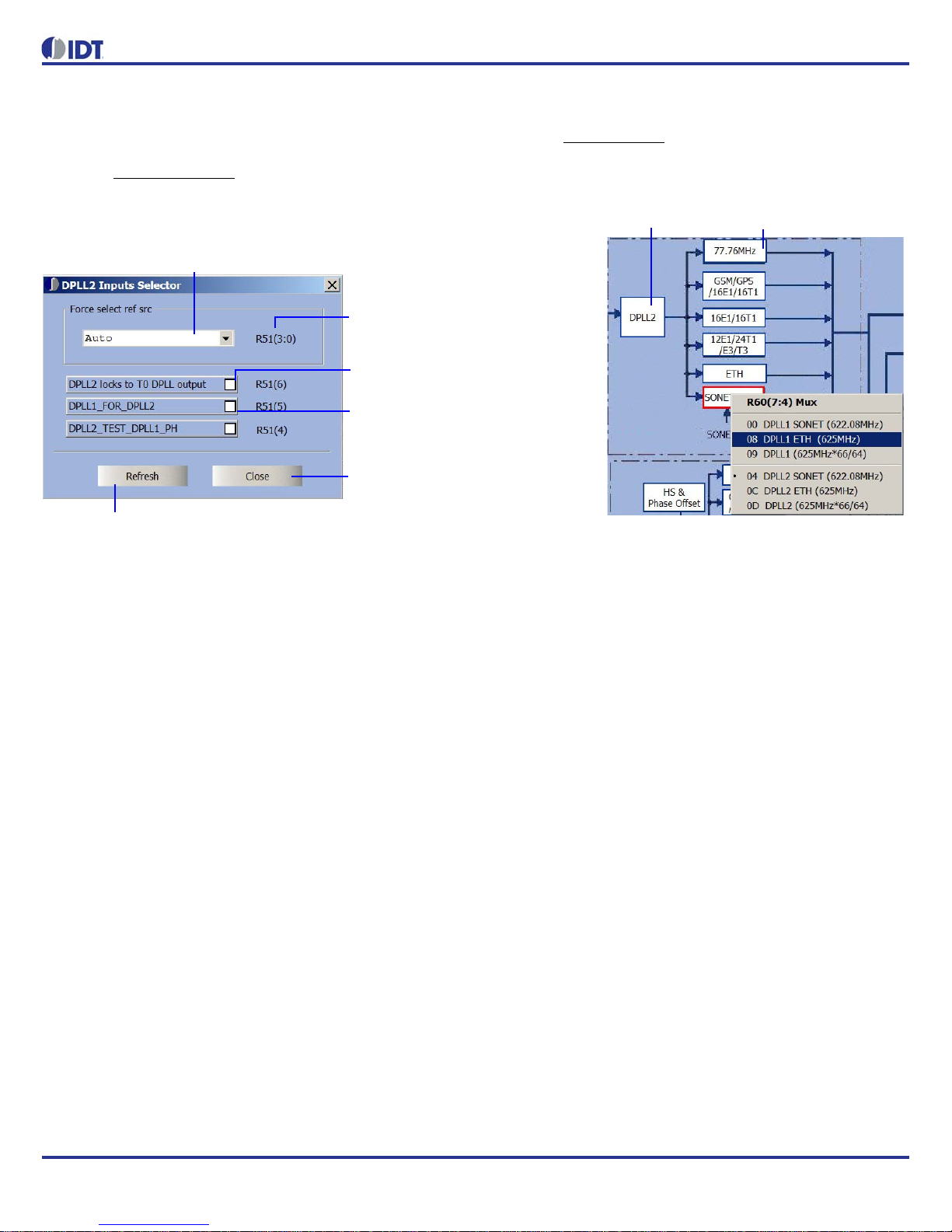
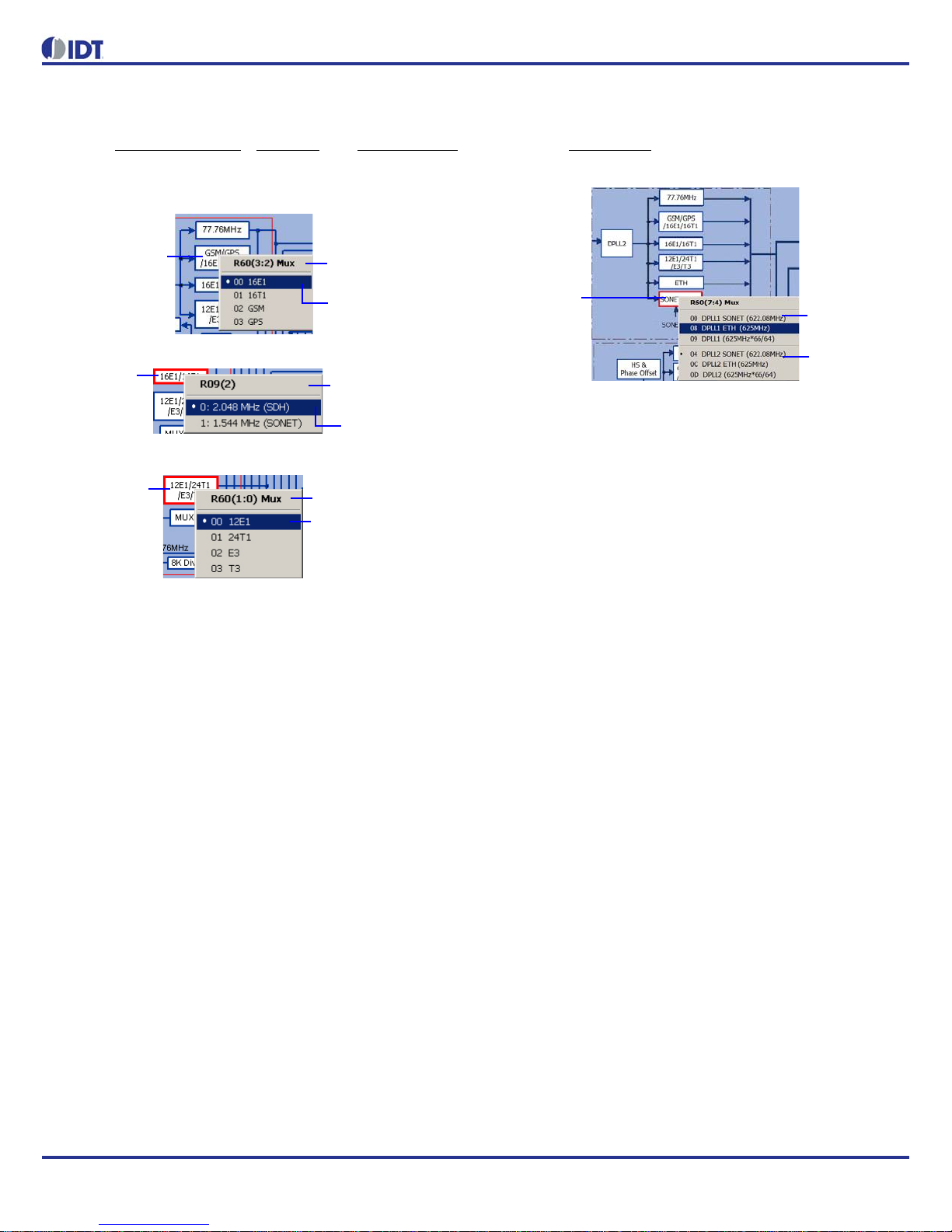
2.6.1 DPLL2 Input Selector...........................................................................................................................13
2.6.2 DPLL2 DPLL.........................................................................................................................................13
2.6.3 DPLL2 DCO Output Clock Frequency Selection..................................................................................14
2.6.4 DPLL2 SONET/GETH Configuration....................................................................................................14
2.7 DPLL1 PATH CONFIGURATION .....................................................................................................................15
2.7.1 DPLL1 Input Selector...........................................................................................................................15
2.7.2 DPLL1...................................................................................................................................................15
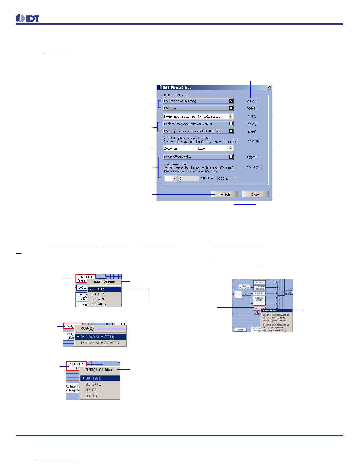
2.7.3 HS and Phase Offset Configuration.....................................................................................................16
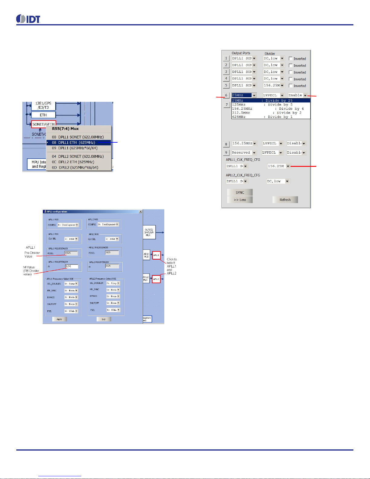
2.7.4 DPLL1 DCO Output Clock Frequency Selection..................................................................................16
2.7.5 DPLL1 SONET/GETH Configuration....................................................................................................16
2.8 OUTPUT PORTS CONFIGURATION ..............................................................................................................17
2.8.1 Ethernet Clock Configuration for Output Ports.....................................................................................18
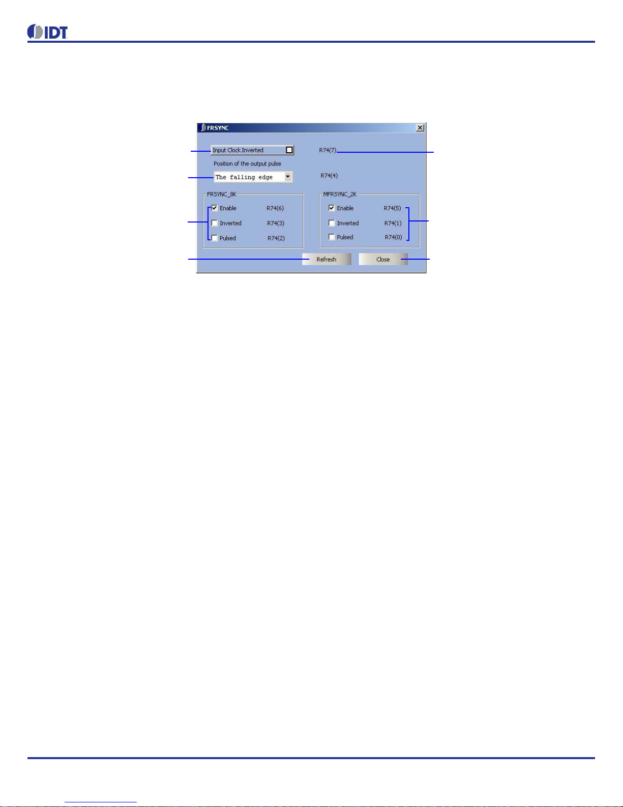
2.8.2 Frame and Multi-Frame Configuration..................................................................................................19
2.9 OTHER CONFIGURATION ..............................................................................................................................20
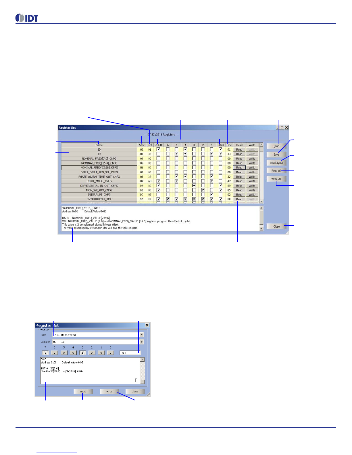
2.9.1 Registers Configuration........................................................................................................................20
2.9.2 Interrupts Configuration........................................................................................................................21
2.10 DPLL STATUS INDICATION ............................................................................................................................22
2.10.1 Current DPLL Status............................................................................................................................22
2.11 PAGE 1 REGISTERS CONFIGURATION ........................................................................................................24
3 APPENDIX: SCHEMATIC FILE ....................................................................................................................................25
TABLE OF CONTENTS

82V3911 WAN PLL
REVISION 1 1/30/15 3EVALUATION BOARD USER’S GUIDE
1 HARDWARE CONFIGURATION
Figure-1 82V3911 Evaluation Board Illustration

82V3911 WAN PLL
EVALUATION BOARD USER’S GUIDE 4REVISION 1 1/30/15
1.1 ANNOTATION FOR FIGURE-1
[1] Output clock 1 - 5
[2] 82V3911 chip
[3] Switch SW5: The function of this switch is described in
Table-1.
[4] Crystal oscillator Master Clock
[5] +5 V DC power supply
[6] +3.3 V power supply for test purpose
[7] +5 V power supply for test purpose
[8] Crystal oscillator for APLL1 and APLL2
[9] OSCI: master clock input
[11] 8 kHz or 1pps frame synchronization output
[12] 2 kHz multi-frame or 1pps frame synchronization output
[13] Output clock 6 (differential)
[14] Output clock 7 (differential)
[15] Output clock 8 (differential)
[16] Output clock 9 (differential)
[17] Input clock to APLL1 (differential)
[18] Input clock to APLL2 (differential)
[19] Input clock 1 (differential)
[20] Input clock 2 (differential)
[21] Input clock 3-6
[22] External frame sync 1 and 2 input
[23] USB communication port
[24] DPLL1 and DPLL2 DPLL lock indicator
[25] Reset button: Press to reset all devices on the board
Table-1 Switch SW5 Function Description
Switch Function Description
SW5-2 SDH/SONET selection Off: SDH
On: SONET
SW5-3 not used
SW5-4~6 not used
SW5-7 I2C_AD1 Off: "0"
On: "1"
SW5-8 I2C_AD2
I2C_AD1 and I2C_AD2 pins
are the address bus of the
microprocessor interface.
Off: "0"
On: "1"

82V3911 WAN PLL
REVISION 1 1/30/15 5EVALUATION BOARD USER’S GUIDE
2 SOFTWARE CONFIGURATION
2.1 INSTALLATION
Double click on the “82V3911 VER1.00_SETUP.exe” file and follow the
screen prompts, you will finish the evaluation software installation. After
the installation, the evaluation software can be launched by choosing
Start>Programs>IDT WAN PLL>IDT WAN PLL 82V3911.
2.2 GENERAL INTRODUCTION
2.2.1 OVERVIEW
The 82V3911 evaluation software provides a friendly interface for users
to configure and control the 82V3911. As shown in Figure-2, the main
window includes:
Menu bar
Shortcut icon
Main work area (the area with blue background)
– Input ports configuration area
– Monitor
– DPLL2 path configuration area
– DPLL1 path configuration area
– Output ports configuration area
– General configuration area
– DPLL1/ DPLL2 path selection and DPLL status indication area
– APLL1/2 configuration
Status bar
To operate this evaluation software, we assume that you have a basic
familiarity with the 82V3911. If you have difficulties in understanding this
users’ manual, please refer to the 82V3911 datasheet.
2.2.2 CONVENTIONS USED
Users can operate this evaluation software by clicking on the menu bar,
theshortcut icons, the functionblocks or the buttons. For easy explanation,
we have adopted a few simple conventions to describe these tools. See
the following table for details.
Name Image (Example) Convention Used
menu bar “Window > Monitor”
shortcut icon shortcut icon
function block “Monitor”
button “Ex Sync”

82V3911 WAN PLL
REVISION 1 1/30/15 6EVALUATION BOARD USER’S GUIDE
Figure-2 Graphic User Interface (GUI)
2.2.3 DPLL1/ DPLL2 PATH SELECTION
Since some registers are related to the input ports, the DPLL1 and the
DPLL2 are shared paths, and users must select a path (DPLL1 or DPLL2)
before configuring these registers. See Figure-3 for details.
Figure-3 DPLL1/ DPLL2 Path Selection
2.2.4 READ/WRITE THE CONFIGURATION DATA
Generally, once a configuration is made, the configuration data will be
directly written to device. But in the Register Set I dialog box, after config-
uring the registers, you need to click the “Write” or “Write All” button to
write the configuration data to device.
In the main work area or in the dialog boxes, you can click on the
“Refresh” button to read the register value from the device.
2.2.5 LOAD/SAVE THE CONFIGURATION DATA
To load or save the configuration data, please open the Register Set I
dialog box by selecting “Windows > Register Set I” or clicking on “MCU
Interface and Registers”. Or you can click on the Load or Save button in
the Main window. Refer to 2.9.1 Registers Configuration for details.
menu bar
shortcut icons
input ports configuration
status bar
DPLL1 & DPLL2 path configuration
DPLL1/ DPLL2 path selection DPLL status indication
output ports configuration
general
configuration
main
work area
click to select DPLL1 or DPLL2
(currently selected: DPLL1 path)

82V3911 WAN PLL
REVISION 1 1/30/15 7EVALUATION BOARD USER’S GUIDE
2.2.6 TIPS FOR THE PARAMETERS AND BUTTONS
The evaluation software provides tips forthe parameters, shortcut icons
and buttons to help users make configurations. For example, when the
mouse focus is on a parameter, a tip will appear displaying the related
register’s name, address and bits. See Figure-4.
Figure-4 Tips for Parameters and Buttons
2.2.7 MENU BAR
The menu bar contains five menus as shown in the following:
File Menu
Figure-5 File Menu
View Menu
Figure-6 View Menu
Tools Menu
Figure-7 Tools Menu
Figure-8 Auto Refresh Configuration
tip for the SYNC button
tip for the division factor
terminate the program
popuptheDeviceand
Mode dialog box close the graphic
user interface (GUI)
toggle the shortcut icons toggle the status bar
toggleautorefreshand
select refresh interval,
see Figure-8
refresh interval selection
toggle auto refresh
(On: the GUI is auto
refreshed in a selected
interval)

82V3911 WAN PLL
REVISION 1 1/30/15 8EVALUATION BOARD USER’S GUIDE
Window Menu
The Window menu contains 13 sub-menus as shown in Figure-9. All
these sub-menus except “Register Set II” and “Hide All Popup” have the
same functions as their respective buttons/function blocks in the main
window. Refer to the corresponding sections for details.
Figure-9 Window Menu
Help Menu
Figure-10 Help Menu
2.2.8 SHORTCUT ICONS
The functions of the shortcut icons are described in the following table:
2.2.9 STATUS BAR
The status bar shows the currently selected microprocessor interface
and communication port. See Figure-11 for details.
Figure-11 Status Bar
pop up the
Register Set II
dialog box, see
Figure-34 hide all pop-up
dialog boxes
provide evaluation
software version and
related information
Shortcut Icon Function
the same as menu “File > Open Device”
the same as menu “Help > About DPLL...”
the same as menu “File > Exit”
selected microprocessor
interface and COM port Indication of communication status
between PC and evaluation board

82V3911 WAN PLL
REVISION 1 1/30/15 9EVALUATION BOARD USER’S GUIDE
2.3 INITIALIZATION
After the program is launched, the Device Port Selection dialog box
pops out as shown in Figure-12. Users can select a COM port in this
dialog box.
Click on “Detect”, and the status of the COM ports will be detected
and displayed in the lower part of this dialog. The evaluation software
will automatically select the port which successfully communicates with
the 82V3911 evaluation board.
Click on “OK”, and the evaluation board will be initialized and the
main window will appear as shown in Figure-2.
Afterinitialization, users can re-open thisdialog box by selecting“File
> Open Device” or clicking on the shortcut icon .
Figure-12 Device Port Selection
2.4 INPUT PORTS STATUS AND CONFIGURATION
The input ports status and configuration interface is as shown in
Figure-13. Users can select frequency and priority for each of the 14
input ports in the corresponding pull-down list. The status of the input
ports are indicated by color LEDs.
Figure-13 Input Configuration (Shrinked)
Click on “More >>”, and the input configuration interface will be
extended to display all input-related status and configuration. See
Figure-14 for details.
click to confirm the configuration
COM ports status indication click to detect COM ports status
COM port selection
priority setting
frequency selection
input clock status
indication
clicktoextend
theinputports
configuration
interface
click to pop up
the Frame
Synchroniza-
tion Control
dialog box

82V3911 WAN PLL
REVISION 1 1/30/15 10 EVALUATION BOARD USER’S GUIDE
Figure-14 Input Configuration (Extended)
input clock status
indication
clock frequency
priority setting DivN divider (checked: used)
lock 8k divider (checked: used)
leaky bucket configuration selection allow/dis-allow lock to the input clock (checked: allow)
input clock quality indication (checked: valid)
register address
and bits
phase loss indication
no activity indication (checked: no activity)
hard frequency alarm indication (checked: has alarm)
click to pop up the
Frame Synchronizing
Control dialog box
revertive mode enable
IN1/IN2 electrical
level selection DivN divider selection
HF divider enable
division factor
click to pop up the
Bucket Configuration
dialog box
click to shrink this input
master clock active edge selection click to read all the
related registers and
refresh the display
configuration interface
(checked: phase loss)
selection

82V3911 WAN PLL
REVISION 1 1/30/15 11 EVALUATION BOARD USER’S GUIDE
2.4.1 LEAKY BUCKET CONFIGURATION
Click on “Buckets” or select “Window > Bucket Window”. The buckets
dialog box pops up as shown in Figure-15. Users can set the four leaky
bucket configurations in this dialog box.
Figure-15 Buckets Dialog Box
2.4.2 FRAME SYNCHRONIZATION CONTROL
Click on “Ex Sync”. The Frame synchronization Control dialog box
pops up as shown in Figure-16. In this dialog box, users can configure the
registers related to the external frame synchronization signal.
Figure-16 Frame Synchronization Control Dialog Box
configuration 0 configuration 1 configuration 2 configuration 3
leaky bucket size
upper threshold
lower threshold
decay rate
slide to change the value
indicate the selected value
register address
click to read the configuration data from the device
click to exit this dialog box
external frame sync. input signal
register address and bits
determine whether the external frame
sync. signal is used
click to read the registers listed in click to exit this dialog box
sampling margin control
external frame sync. signal frequency selection
this dialog box and refresh the display
external frame sync signal monitor range selection

82V3911 WAN PLL
REVISION 1 1/30/15 12 EVALUATION BOARD USER’S GUIDE
2.5 MONITOR CONFIGURATION
Click on “Monitor” or select “Window > Monitor”. The Monitors dialog
box pops up as shown in Figure-17. In this dialog box, users can configure
the input clock quality monitor.
Figure-17 Monitors Dialog Box
register address and bits
operation status indication
DPLL1/DPLL2 hard frequency alarm limit
click to read all registers
listed in this dialog box click to pop up the Buckets Configuration dialog box
click to exit this dialog box
frequency measurement of the
hard frequency alarm configuration
selected input clock
frequency monitors clocked by master
phase lock alarm is cleared by
software or timeout
clock / output clock from the DPLL1
(checked: master clock)
checked: phase loss alarm is
triggered when DPLL1/DPLL2
threshold
checked: DPLL1_MAIN_REF_FAILED
interrupt flagged on the TDO pin
(checked: time out)
timeout value
multi factor
reaches the hard frequency alarm

82V3911 WAN PLL
REVISION 1 1/30/15 13 EVALUATION BOARD USER’S GUIDE
2.6 DPLL2 PATH CONFIGURATION
2.6.1 DPLL2 INPUT SELECTOR
Click on “DPLL2 Input Selector” or select “Window > DPLL2 Input”. The
following dialog box pops out, allowing users to select an input to the
DPLL2.
Figure-18 DPLL2 Input Selector Dialog Box
2.6.2 DPLL2 DPLL
Click on “DPLL2 PFD & LP” or select “Window > DPLL2”. The DPLL2
dialog box pops out as shown in Figure-19. This dialog box allows users to
configure the DPLL2.
Figure-19 DPLL2 Dialog Box
Note: Before opening this dialog box, users must select the DPLL2
path (see 2.2.3 DPLL1/ DPLL2 Path Selection), otherwise the DPLL2
coarse/fine phase detector can not be configured.
click to read register R51 and refresh the display of this dialog
DPLL2 input clock selection when DPLL2 locks independently from DPLL1
DPLL2 lock/not lock to
(checked: lock to T0)
lock to 8k or 77.76M
(checked: 8k)
register address
and bits
click to exit this dialog
DPLL2 operating mode selection register address and bits

82V3911 WAN PLL
REVISION 1 1/30/15 14 EVALUATION BOARD USER’S GUIDE
2.6.3 DPLL2 DCO OUTPUT CLOCK FREQUENCY SELECTION
Click on “GSM/GPS/16E1/16T1”, “16E1/16T1” and “12E1/24T1/E3/T3”
in the DPLL2 path to select the DCO output clock frequency. See Figure-
20 for details.
Figure-20 DPLL2 DCO Output Frequency Selection
2.6.4 DPLL2 SONET/GETH CONFIGURATION
Click on “SONET/GETH” to select an input source for the DPLL2
SONET/GETH. See Figure-21.
Figure-21 DPLL2 SONET/GETH Input Source Selection
click to select
GSM/GPS/16E1/16T1 register address
and bits
16E1 selected
click to select
16E1/16T1 register address
and bit
2.048 MHz selected
click to select
12E1/24T1/E3/T3 register address and bits
12E1 selected
click to select
an input source
for DPLL2 APLL register address
and bits
DPLL2 77.76 MH
selected

82V3911 WAN PLL
REVISION 1 1/30/15 15 EVALUATION BOARD USER’S GUIDE
2.7 DPLL1 PATH CONFIGURATION
2.7.1 DPLL1 INPUT SELECTOR
Click on “DPLL1 Input Selector” or select “Window > DPLL1 Input”. The
following dialog box pops out, allowing users to select an input for the
DPLL1.
Figure-22 DPLL1 Input Selector Dialog Box
2.7.2 DPLL1
Click on “DPLL1 PFD & LP” or select “Window > DPLL1”. The DPLL1
dialog box pops out as shown in Figure-23. This dialog box allows users to
configure the DPLL1.
Note: Before opening this dialog box, users must select the DPLL1
path (see 2.2.3 DPLL1/ DPLL2 Path Selection), otherwise the DPLL1
coarse/fine phase detector can not be configured.
Figure-23 DPLL1 Dialog Box
register address and bits
DPLL1 Auto/Forced input clock selection
DPLL1 Internal Fast/Slow input clock selection
(checked:
Internal Fast Selection)
check to enable DPLL1 External Fast Switching
click to read the registers listed in this dialog box
click to exit this dialog box
DPLL1 operation
mode indication
DPLL1 bandwidth
and damping factor
configuration
DPLL1 holdover
mode configuration
DPLL1 coarse phase lock detector
configuration
DPLL1 fine phase lock detector
configuration
click to read the registers click to exit this dialog box
currently selected
path indication
DPLL1 operation
mode selection
DPLL1 Mini-Holdover
mode configuration
DPLL1 holdover frequency
configuration when in Manual
Holdover mode
listed in this dialog box

82V3911 WAN PLL
REVISION 1 1/30/15 16 EVALUATION BOARD USER’S GUIDE
2.7.3 HS AND PHASE OFFSET CONFIGURATION
Click on “HS & Offset” or select “Window > HS Phase Offset”. The HS
and Phase Offset dialog box pops out as shown in Figure-24. This dialog
box allows users to configure HS & phase offset.
Figure-24 HS and Phase Offset Dialog Box
2.7.4 DPLL1 DCO OUTPUT CLOCK FREQUENCY SELECTION
Click on “GSM/OBSAI/16E1/16T1”, “16E1/16T1” and “12E1/24T1/E3/
T3” in the DPLL1 path to select the DCO output clock frequency. See
Figure-25 for details.
Figure-25 DPLL1 DCO Output Frequency Selection
2.7.5 DPLL1 SONET/GETH CONFIGURATION
Click on “DPLL1 SONET/GETH” to select an input source for the
DPLL1 APLL. See Figure-26.
Click on “DPLL1 SONET/GETH” to select a bandwidth for the DPLL1
APLL. See Figure-27.
Figure-26 DPLL1 SONET/GETH Input Source Selection
register address and bits
phase transient limit configuration
click to read the registers
click to exit this dialog box
listed in this dialog box
input clock to output clock
phase offset configuration
HS configuration when
input clock switches
HS triggered when phase error
is outside the phase transient limit
register address
click to select
ETH/3G_BTS/16E1/16T1
16 E1 selected
and bits
register address
click to select
16E1/16T1 and bits
register address
click to select
12E1/24T1/E3/T3 and bits
register address
and bits
click to select
an input source
for DPLL1 SONET/
GETH

82V3911 WAN PLL
REVISION 1 1/30/15 17 EVALUATION BOARD USER’S GUIDE
2.8 OUTPUT PORTS CONFIGURATION
The default output ports configuration interface is as shown in Figure-
27. Click on “<< More”, and this interface extends to show all output-
related configuration information. See Figure-28 for details.
Figure-27 Output Ports Configuration (Shrinked) Figure-28 Output Ports Configuration (Extended)
output port number
frequency selection
Out6 LVDS/PECL
click to pop up the
Out7 LVDS/PECL
click to extend this output ports configuration interface
electrical level selection
FRSYNC dialog box
division factor selection of the output clock
checked: output inverted
click to shrink this output port
click to refresh the display
configuration interface
of this dialog box

82V3911 WAN PLL
REVISION 1 1/30/15 18 EVALUATION BOARD USER’S GUIDE
2.8.1 ETHERNET CLOCK CONFIGURATION FOR OUTPUT
PORTS
Following is an example using Ethernet clocks from the DPLL1
SONET/GETH (625 MHz) path to configure the output 6. The steps
below are performed from the main GUI (refer to Figure-2).
1. Click on "DPLL1 SONET/GEHT" to select "08 DPLL1 ETH (625
MHz)".
Figure-29 Selecting a DPLL1 Input Source
2.Clickon "APLL1" or "APLL2" to configuretheAPLL interface, and
setting "19525" to PDSEL and "3124" to M
Figure-30 APLL Configuration Interface
3. Click on "<< More" in the output ports configuration interface to
show all output-related configuration information. Click on output
6 in the output ports configuration interface to select "25MHz/
125MHz/ 156.25MHz/ 312.5MHz/ 625MHz". The "Enable Output"
and "156.25MHz" clock on DPLL1 SONET/GETH Path should be
selected.
Figure-31 DPLL1 APLL1 ETH Clock Selection for
Output 6
Select “08 DPLL1 ETH
(625 MHz)”
Enable Output
Select
156.25MHz
clock on
DPLL1
SONET/GETH
path
Select ETH
clock on OUT6

82V3911 WAN PLL
REVISION 1 1/30/15 19 EVALUATION BOARD USER’S GUIDE
2.8.2 FRAME AND MULTI-FRAME CONFIGURATION
Click on “SYNC” or select “Window > Output Frame Sync”. The Frame
and Multi-Frame configuration dialog box pops up as shown in Figure-32.
Figure-32 Frame/Multi-Frame Configuration Dialog Box
checked: 2 kHz/4 kHz/8 kHz register address and bits
input clock inverted
FRSYNC_8K output configuration MFRSYNC_2K output configuration
click to read the registers
listed in this dialog box click to exit this dialog box
FRSYNC_8K & MFRSYNC_2K
output pulse position configuration

82V3911 WAN PLL
REVISION 1 1/30/15 20 EVALUATION BOARD USER’S GUIDE
2.9 OTHER CONFIGURATION
2.9.1 REGISTERS CONFIGURATION
Register Set I Dialog Box
Click on “MPU Interface and Registers” or select “Window > Register
Set I”. The Register Set dialog box pops up as shown in Figure-33.
Users can configure all registers or check the status of all registers in
this dialog box. Users can save the register configuration data as a file
(*.rgf) for later use, or load the configuration data from a file.
Figure-33 Register Set I Dialog Box
Register Set II Dialog Box
Select “Window > Register Set II”. The Register Set II dialog pops up
as shown in Figure-34. This dialog box provides a convenient way to
access a group of registers that have related functions.
Figure-34 Register Set II Dialog Box
register name
register address
default value of the register register bits (b7-b0) register value display/input
read the value of the corresponding
(checked: the bit is set to “1”)
write configuration
load configuration data
save configuration
read register value
from the device
data to the device
adjust the layout
of this dialog box
description of the current-selected register
currently selected
register
exit this dialog box
data as a file
(double-click to input the register value) from a file
register from the device
select a group of select a register in
the selected group
registers to configure value of the
selected register
read the register value
selected register
description of the from the device write the configured
value to the register
Table of contents
Other IDT Motherboard manuals

IDT
IDT 82P33714 User manual

IDT
IDT 8A34 Series User manual

IDT
IDT EB8T5A Eval Board User manual

IDT
IDT Tsi340-RDK1 User manual

IDT
IDT Tsi84 User manual

IDT
IDT 89EBPES12N3 User manual

IDT
IDT P9221-R-EVK User manual

IDT
IDT P9242-G-EVK User manual

IDT
IDT 89EBPES16T4G2 User manual

IDT
IDT 9FGV1005 Operating instructions

IDT
IDT ZNRG2061 User manual

IDT
IDT EB-LOGAN-23 User manual

IDT
IDT 8T49N24 Series Installation and operating instructions

IDT
IDT P9241-G-EVK User manual

IDT
IDT ZMOD4410 User manual

IDT
IDT 5P49V5907 Manual

IDT
IDT VersaClock 6E 5P49V6965 User manual

IDT
IDT VersaClock 3S User manual

IDT
IDT Tsi382 LQFP User manual

IDT
IDT ADC1410S Series User manual