10 Datasheet
Introduction
1.1 Terminology
A ‘#’ symbol after a signal name refers to an active low signal, indicating a signal is in the active
state when driven to a low level. For example, when RESET# is low, a reset has been requested.
Conversely, when NMI is high, a nonmaskable interrupt has occurred. In the case of signals where
the name does not imply an active state but describes part of a binary sequence (such as address or
data), the ‘#’ symbol implies that the signal is inverted. For example, D[3:0] = ‘HLHL’ refers to a
hex ‘A’, and D[3:0]# = ‘LHLH’ also refers to a hex ‘A’ (H= High logic level, L= Low logic level).
“FSB” refers to the interface between the processor and system core logic (i.e., the chipset
components). The FSB is a multiprocessing interface to processors, memory, and I/O.
1.1.1 Processor Packaging Terminology
Commonly used terms are explained here for clarification:
•Intel®Pentium®4 processor on 90 nm process — Processor in the FC-mPGA4 package
with a 1-MB L2 cache.
•Processor — For this document, the term processor is the generic form of the Pentium 4
processor on 90 nm process.
•Keep-out zone — The area on or near the processor that system design cannot use.
•Intel® 865G/865GV/865PE/865P chipset — Chipset that supports DDR memory technology
for the Pentium 4 processor on 90 nm process.
•Intel® 875P chipset — Chipset that supports DDR memory technology for the Pentium 4
processor on 90 nm process
•Processor core — Processor core die with integrated L2 cache.
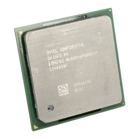
•FC-mPGA4 package — The Pentium 4 processor on 90 nm process is available in a Flip-
Chip Micro Pin Grid Array 4 package, consisting of a processor core mounted on a pinned
substrate with an integrated heat spreader (IHS). This packaging technology employs a
1.27 mm [0.05 in] pitch for the substrate pins.
•mPGA478B socket — The Pentium 4 processor on 90 nm process mates with the system
board through a surface mount, 478-pin, zero insertion force (ZIF) socket.
•Integrated heat spreader (IHS) —A component of the processor package used to enhance
the thermal performance of the package. Component thermal solutions interface with the
processor at the IHS surface.
•Retention mechanism (RM)—Since the mPGA478B socket does not include any mechanical
features for heatsink attach, a retention mechanism is required. Component thermal solutions
should attach to the processor via a retention mechanism that is independent of the socket.
•Storage conditions — Refers to a non-operational state. The processor may be installed in a
platform, in a tray, or loose. Processors may be sealed in packaging or exposed to free air.
Under these conditions, processor pins should not be connected to any supply voltages, have
any I/Os biased, or receive any clocks. Upon exposure to “free air”(i.e. unsealed packaging or
a device removed from packaging material) the processor must handled in accordance with
moisture sensitivity labeling (MSL) as indicated on the packaging material.
•Functional operation — Refers to normal operating conditions in which all processor
specifications, including DC, AC, FSB, signal quality, mechanical and thermal, are satisfied.

