JETWAY 613CN User manual

613CN/613CF/611CN/611CF
USER'S MANUAL
M/B For Socket 370 Pentium
IIIProce or
NO. G03-613CFR2A
Release date: April 2001
Trademark:
* Pentium is registered trademark and MMX is a trademark of Intel Corporation,
t e ot er names and brands are t e property of t eir respective owners
* Specifications and Information contained in t is documentation are furnis ed for information use only, and are
subject to c ange at any time wit out notice, and s ould not be construed as a commitment by manufacturer.

USER’S NOTICE.............................................................................ii
MANUAL REVISION INFORMATION............................................1
THERMAL SOLUTIONS.........................................................................................1
CHAPTER 1 INTRODUCTION OF 613CN/613CF/611CN/611CF
MOTHERBOARD
1-1 FEATURE OF MOTHERBOARD...............................................................2
1-2 SPECIFICATION...........................................................................................3
1-3 PERFORMANCE LIST.................................................................................4
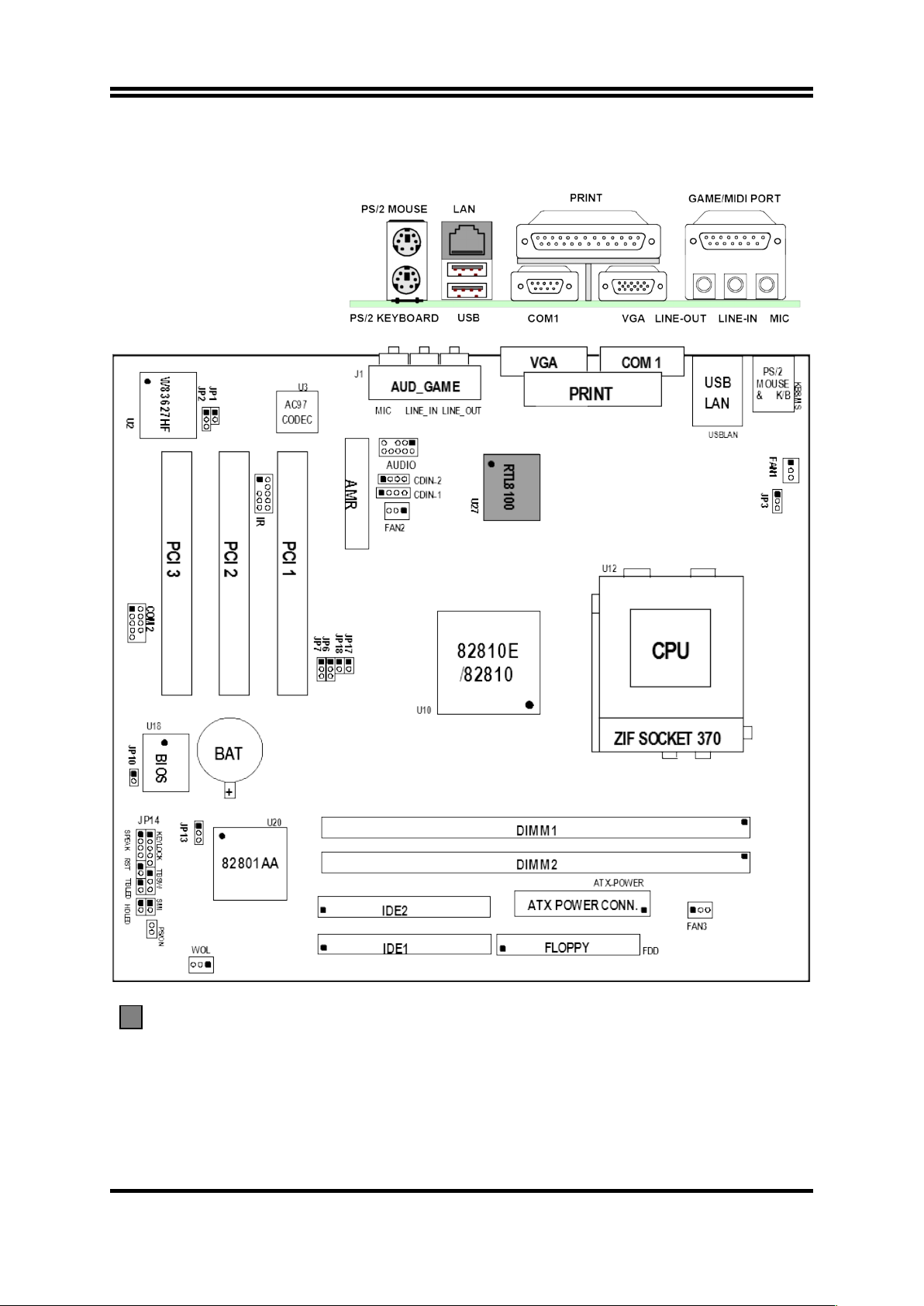
1-4 LAYOUT DIAGRAM & JUMPER SETTING............................................5
CHAPTER 2 HARDWARE INSTALLATION
2-1 HARDWARE INSTALLATION STEPS......................................................7
2-2 CHECKING MOTHERBAORD'S JUMPER SETTING...........................7
2-3 INSTALL CPU................................................................................................9
2-3-1 ABOUT PENTIUM & CELERON™ 370-PIN CPU...............................9
2-3-2 SETTING CPU BUS CLOCK & MEMORY CLOCK JUMPER.............9
2-3-3 INSTALL CPU..............................................................................................10
2-3-4 OVERCLOCK RUNNING..........................................................................11
2-4 INSTALL MEMORY.....................................................................................13
2-5 EXPANSION CARD.......................................................................................14
2-5-1 PROCEDURE FOR EXPANSION CARD INSTALLATION..................14
2-5-2 ASSIGNING IRQ FOR EXPANSION CARD............................................14
2-5-3 INTERRUPT REQUEST TABLE FOR THIS MOTHERBOARD..........15
2-6 CONNECTORS, HEADERS.........................................................................15
2-6-1 CONNECTORS............................................................................................15
2-6-2 HEADERS.....................................................................................................19
2-7 STARTING UP YOUR COMPUTER..........................................................22
CHAPTER 3 INTRODUCING BIOS
3-1 ENTERING SETUP.......................................................................................23
3-2 GETTING HELP............................................................................................24
3-3 THE MAIN MENU.........................................................................................24
3-4 STANDARD CMOS FEATURES.................................................................26
3-5 ADVANCED BIOS FEATURES...................................................................27
3-6 ADVANCED CHIPSET FEATURES...........................................................30
3-7 INTEGRATED PERIPHERALS..................................................................31
3-7-1 ONBOARD IDE FUNCTION......................................................................32
3-7-2 ONBOARD PCI DEVICE............................................................................33
3-7-3 WINBOND SUPERIO DEVICE..................................................................34
3-8 POWER MANAGEMENT SETUP..............................................................35
3-8-1 RELOAD TIMER EVENTS........................................................................37
3-9 PNP/PCI CONFIGURATION SETUP.........................................................38
i
TABLE OF CONTENT

3-10 PC HEALTH STATUS.................................................................................39
3-11 MISCELLANEOUS CONTROL.................................................................40
3-12 LOAD STANDARD/OPTIMIZED DEFAULTS........................................40
3-13 SET SUPERVISOR/USER PASSWORD....................................................41
CHAPTER 4 DRIVER & FREE PROGRAM INSTALLATION
MAGIC INSTALL SUPPORTS WINDOWS 95/98/98SE/NT4.0/2000..............42
4-1 INF INSTALL INTEL 10E/ 10 CHIPSET SYSTEM DRIVER......................43
4-2 IDE INSTALL ULTRA ATA33 OR ULTRA ATA 66 DRIVER.......................44
4-3 VGA INSTALL ON-BOARD VGA DRIVER....................................................45
A. For WINDOWS 95/9 /9 SE/NT4.0..................................................45
B. For WINDOWS 2000.......................................................................46
4-4 PC-HEALTH INSTALLS PC HEALTH MONITOR IIII SOFTWARE FOR
HARDWARE MONITORING DEVICE....................................47
4-5 AC97 SOUND DRIVER AND THE PROGRAM INSTALL FOR
EDITING/PLAYBACK..................................................................................48
4-6 LAN (ONLY FOR 613CF/611CF)
INSTALL 10/100M PCI FAST ETHERNET DRIVER..............49
4-7 PC-CILLIN INSTALL PC-CILLIN 2000 ANTI-VIRUS PROGRAM............50
4-8 HOW TO UTILIZE ALSRACK EDITING & PLAYBACK UTILITY. ..51
4-9 HOW TO UTILIZE PC-HEALTH...............................................................52
4-10 HOW TO DISABLE ON-BOARD SOUND.................................................53
4-11 HOW TO UPDATE BIOS..............................................................................53
USER’S NOTICE
COPYRIGHT OF THIS MANUAL BELONGS TO THE MANUFACTURER. NO PART OF
THIS MANUAL, INCLUDING THE PRODUCTS AND SOFTWARE DESCRIBED IN IT
MAY BE REPRODUCED, TRANSMITTED OR TRANSLATED INTO ANY LANGUAGE IN
ANY FORM OR BY ANY MEANS WITHOUT WRITTEN PERMISSION OF THE
MANUFACTURER.
THIS MANUAL CONTAINS ALL INFORMATION REQUIRED TO USE 613CN/613CF/
611CN/611CF MOTHER-BOARD AND WE DO ASSURE THIS MANUAL MEETS USER’S
REQUIREMENT BUT WILL CHANGE, CORRECT ANY TIME WITHOUT NOTICE.
MANUFACTURER PROVIDES THIS MANUAL “AS IS” WITHOUT WARRANTY OF ANY
KIND, AND WILL NOT BE LIABLE FOR ANY INDIRECT, SPECIAL, INCIDENTIAL OR
CONSEQUENTIAL DAMAGES (INCLUDING DAMANGES FOR LOSS OF PROFIT, LOSS OF
BUSINESS, LOSS OF USE OF DATA, INTERRUPTION OF BUSINESS AND THE LIKE).
PRODUCTS AND CORPORATE NAMES APPEARING IN THIS MANUAL MAY OR MAY
NOT BE REGISTERED TRADEMARKS OR COPYRIGHTS OF THEIR RESPECTIVE
COMPANIES, AND THEY ARE USED ONLY FOR IDENTIFICATION OR EXPLANATION
AND TO THE OWNER’S BENEFIT, WITHOUT INTENT TO INFRINGE.
ii

Manual Revision Information
Reversion Revision History Date
2.0 Second Edition April 2001
Item Checklist
613CN/613CF/611CN/611CF Motherboard
Cable for IDE/Flopp
CD for motherboard utilities
Cable for COM2
613CN/613CF/611CN/611CF User’s Manual
Intel Processor Family
Thermal Solutions
As processor technolog pushes to faster speeds and higher performance, thermal
management becomes increasingl crucial when building computer s stems.
Maintaining the proper thermal environment is ke to reliable, long-term s stem
operation. The overall goal in providing the proper thermal environment is keeping the
processor below its specified maximum case temperature. Heatsinks induce improved
processor heat dissipation through increased surface area and concentrated airflow
from attached fans. In addition, interface materials allow effective transfers of heat
from the processor to the heatsink. For optimum heat transfer, Intel recommends the
use of thermal grease and mounting clips to attach the heatsink to the processor.
When selecting a thermal solution for our s stem, please refer to the website below
for collection of heatsinks evaluated and recommended b Intel for use with Intel
processors.
Vendor list for heatsink and fan of Pentium® !!! processor, please visit:
http://developer.intel.com/design/Pentiumiii/components/index.htm
Vendor list for heatsink and fan of Intel®Celeron™ processor, please visit:
http://developer.intel.com/design/celeron/components/index.htm
1

Chapter 1
Introduction of 613CN/613CF/611CN/611CF
Motherboard
1-1 Feature of motherboard
The 613CN/613CF/611CN/611CF motherboard is design for use Intel’s new
generation Pentium processors, which utilize the Socket 370 design and the memor
size expandable to 512MB (using 128Mb technolog ). This motherboard integrated
VGA, Audio, PC Health, and LAN (onl for 613CF/611CF) Function with Micro ATX
form factor to support total solution for toda ’s computer market.
611CN/611CF using Intel 810 chipset, support 66/100MHz Front Side Bus
613CN/613CF using Intel 810E chipset, whose 133MHz front side bus delivers a clear
upgrade path to the future generation of 133MHz processors and PC-100/PC-133
SDRAM. The 613CN/613CF/611CN/611CF motherboard offers ULTRA DMA 66
(ATA 66) to provide speedier HDD throughout that boosts overall s stem
performance.
The 613CN/613CF/611CN/611CF also has an integrated AC’97 2.1 CODEC on board
which is full compatible with Sound Blaster Pro that gives ou the best sound
qualit and compatibilit . 810E chipset also includes integrated 3D Graphic
Acceleration to provide a lower cost video displa solution.
With USB control as well as capabilit of expanding to 2 USB connectors, the 613CN/
613CF/611CN/611CF meet future USB demand. Moreover, it has built-in hardware
monitor function to monitor and protect our computer.
This motherboard provides high performance & meets future specification demand. It
is reall wise choice for our computer.
2

1-2 Specification
Spec Description
Design Micro ATX form factor 4 la ers PCB size: 24.5 x 22.0 cm
C ipset INTEL 810E Chipset for 613CN/613CF to support up to
133MHz F.S.B.
INTEL 810 Chipset for 611CN/611CF to support up to
100MHz F.S.B.
Clock Generator Winbond W83194R-We
Support 66/100/133MHz s stem Bus Clock (CPU Bus Clock)
Support 100 MHz s stem memor clock
Support 33MHz PCI Bus clock
CPU Socket Support Pentium III 5001GHz processor
Support Celeron 300900MHz processor
Support 66, 100 and 133MHz CPU Bus clock
Reserves support for future Intel Pentium III processors
Support C rix III series processors
Memory Socket 168-pin DIMM socket x2
PC-100/PC-133 SDRAM
Expandable to 512MB
Support 3.3V SDRAM DIMM
Expansion Slot
& Headers
32-bit PCI slot x3
AMR slot x1
Integrate VGA 3D graphic acceleration
Integrate IDE 2 channel of Bus Master IDE port supporting ULTRA DMA
33/66 mode devices
Audio AC’97 Digital Audio controller integrated
AC’97 Audio CODEC on board
Audio driver and utilit included
LAN (Only for
613CF/611CF)
On Board RTL8100 PCI LAN controller
Support 10/100 Base T Transfer rate
BIOS Award 2Mb Flash ROM
Multi I/O PS/2 ke board and PS/2 mouse connectors
Flopp disk drive connector x1
Parallel port x1
Serial port x2
USB connector x2
Audio connector (Line-in, Line-out/MIC & Game Port)
3

1-3 Performance List
The following performance data list is the testing result of some popular benchmark
testing programs. These data are just referred b users, and there is no responsibilit
for different testing data values gotten b users (the different Hardware & Software
configuration will result in different benchmark testing results.)
CPU: Intel PIII 866MHz FC-PGA package
DRAM: 128M SDRAM x2 (H undai GM 72V66841ET75)
VGA Expansion Card: Geforce 256 (1024x768 Hi-color) Driver V3.68
Hard Disk Driver: Quantum Fireball KX20A11
BIOS: Award Optimal default
OS: Win 98SE
Performance Test Report
Coppermine 866MHz
3D Mark 99 1660
3D Winbenc 99 V1.2 301
3D Winbenc 2000 5.33
Final Reality 5.25
Winstone 99 V1.3 30.8
Winstone 2000 31.9
Winbenc 99 :
CPU Mark 99 69.7
FPU Winmark 99 4610
Business Disk Winmark99 4970
Hi-end Disk Winmark99 17000
Business Graphic Winmark 192
Hi-end Graphic Winmark 734
SYS Mark 2000 : SISMark 2000 Rating (Internet Content Creation / Office
Productivity)
Suites 158 (160/157)
Official 158 (159/157)
SISOFT Sandra 2000 :
CPU MIPS 2357
FPU MFLOPS 1167
CPU / Memor MB/S 202
FPU / Memor MB/S 209
4

1-4 Layout Diagram & Jumper Setting
Only for 613CF/611CF
Jumper
5

Jumper Name Description Page
JP6, JP7,
JP17, JP18
CPU & SDRAM Frequenc Setting 3-pin Block
2-pin Block
p.7
JP3 Ke board Power ON Function Setting 3-pin Block p.7
JP2 Clear Ke board Power On Password Setting 3-pin Block p.8
JP13 CMOS RAM Clear 3-pin Block p.8
JP10 BIOS boot block lock 2-pin Block p.8
Connectors
Connector Name Description Page
ATX-POWER ATX Power Connector 20-pin Block p.15
KB&MS PS/2 Mouse & PS/2 Ke board Connector 6-pin Female p.15
USBLAN USB Port Connector
LAN Connector (Onl for 613CF/611CF)
4-pin Connector
RJ45 Connector
p.16
PRINT Parallel Port Connector 25-pin Female p.16
VGA VGA Port Connector 15-pin Female p.17
AGC Audio/Game Connector 3 phone jack+15-pin
Connector
p.17
COM1 Serial Port COM1 Connector 9-pin Connector p.17
FDD Flopp Driver Connector 34-pin Block p.17
IDE1 Primar IDE Connector 40-pin Block p.18
IDE2 Secondar IDE Connector 40-pin Block p.18
Headers
Header Name Description Page
COM2 COM2 Headers 9-pin Block p.19
AUDIO External Line-In/Line-out/MIC header 9-pin Block
HDLED IDE activit LED 2-pin Block p.19
TBLED Turbo LED switch 2-pin Block p.19
RST Reset switch lead 2-pin Block p.19
KEYLOCK Ke board lock switch 2-pin Block p.19
SPEAK Speaker connector 4-pin Block p.19
PWR LED Power LED 2-pin Block p.20
PS/ON Power switch 2-pin Block p.20
FAN1, FAN2, FAN3 FAN Speed Headers 3-pin Block p.20
IR IR infrared module Headers 9-pin Block p.20
CDIN-1, CDIN-2 CD Audio-In Headers 4-pin Block p.21
WOL Wake On LAN Connector 3-pin Block p.21
Expan ion Socket
Socket/Slot Name Description Page
ZIF Socket 370 CPU Socket 370-pin FC-PGA/PPGA CPU Socket p.10
DIMM1, DIMM2 DIMM Module Socket 168-pin DIMM Module Socket p.13
PCI1, PCI2, PCI3 PCI Slot 32-bit PCI Local Bus Expansion slots p.14
AMR AMR Slot Support Audio Modem Riser Card
Chapter 2
Hardware installation
6

2-1 Hardware installation Steps
Before using our computer, ou had better complete the following steps:
1. Check motherboard setting
2. Install CPU
3. Install Memor
4. Install Expansion cards
5. Connect Ribbon cables, Panel wires, and power suppl
6. Setup BIOS
7. Install software driver & utilit
2-2 Checking Motherboard’s Jumper Setting
1. CPU & SDRAM Clock setting : JP6, JP7, JP17, JP18
The motherboard’s CPU & SDRAM memory clock adjusted throu h jumper JP6,
JP7, JP17, JP18 Table as below:
CPU/SDRAM (MHz) JP6 JP7 JP17 JP18
AUTO 1-2 1-2 ON ON * Default
66/100 2-3 2-3 OFF OFF
100/100 2-3 1-2 OFF OFF
133/100
Onl for 613CN/613CF
1-2 1-2 OFF OFF
2. Keyboard Power On Function setting (3-pin): JP3
This allows ou to disable the ke board power on function. Set the jumper to
enabled or disabled if ou wish to use our ke board (b pressing < >) to power on
our computer, this feature requires an ATX power suppl that can suppl at least
300mA on the +5VSB lead. The default is set on disable.
3. Clear Keyboard Power On password setting (3-pin): JP2
7

You can set ke board power on function password to assure computer securit to
setting password through BIOS SETUP, and ou can clear ke board power on
password b JP2.
4. CMOS RAM Clear (3-pin): JP13
A batter must be used to retain the motherboard configuration in CMOS RAM
short 1-2 pins of JP13 to store the CMOS data.
Note: You can clear CMOS by horting 2-3 pin, while the y tem i off. Then
return to 1-2 pin po ition. Avoid clearing the CMOS while the y tem i
on, it will damage the motherboard alway unplug the power cord from
the wall ocket.
5. BIOS Boot Block Lock (2-pin): JP10
This jumper let ou choose when upgrade BIOS can lock Boot Block, to protect
s stem can boot when upgrade BIOS fail.
2-3 Install CPU
8

2-3-1 About Pentium III & Celeron™ 370-pin CPU
This motherboard supports both Pentium III & Celeron 370 pins CPU.
T e way to recognize t e specification of CPU from t e packing Pentium III 370
pins FC-PGA
On the surface of the CPU as shown on the right picture, under the word of
“PENTIUM III” the code is:
RB 0526 P2 66 256
RB : FC–PGA packing
P2 : P2–133MHz front side bus frequenc
PY–100MHz front side bus frequenc
866 : CPU internal frequenc , where here is
866MHz
256 : the size of L2 cache, where here is 256K
Celeron FC–PGA
On the surface of the CPU as shown on the right picture, under the word of “Celeron”
the code is:
566/128/66/1.5V
566 : CPU internal frequenc , where here is 566MHz
128 : the size of L2 cache, where here is 128K
66 : front side bus frequenc , where here is 66MHz
1.5V : the voltage for the CPU
2-3-2 Setting CPU Bus Clock & Memory Clock Jumper
Setting t e front side bus frequency and SDRAM frequency
The motherboard uses jumper JP6, JP7, JP17 and JP18 for the front side bus
frequency and SDRAM frequency settin as shown from the table below:
CPU/SDRAM (MHz) JP6 JP7 JP17 JP18
AUTO 1-2 1-2 ON ON * Default
66/100 2-3 2-3 OFF OFF
100/100 2-3 1-2 OFF OFF
133/100 1-2 1-2 OFF OFF
Example: Using a Pentium III 866 CPU wit front side bus frequency of 133MHz
and PC-133 SDRAM module, t e setting of JP6, JP7 will be all 1-2, and
9

JP17, JP18 all off (open). Will form CPU BUS CLOCK be 133MHz and
SDRAM CLOCK be 100MHz.
For experience u er looking for over clocking, plea e refer to ec 2-3-4
2-3-3 Install CPU
This motherboard provides a ZIF socket 370. The CPU that comes with the
motherboard should have a cooling FAN attached to prevent overheating. If this is not the
case, then purchase a correct cooling FAN before ou turn on our s stem.
WARNING! Be sure that there is sufficient air circulation across the processor’s
heatsink and CPU cooling FAN is working correctl , otherwise it
ma cause the processor and motherboard overheat and damage, ou
ma install an auxiliar cooling FAN, if necessar .
To install a CPU, first turn off our s stem and remove its cover. Locate the ZIF
socket and open it b first pulling the level sidewa s awa from the socket then
upward to a 90-degree angle. Insert the CPU with the correct orientation as shown
below. The notched corner should point toward the end of the level. Because the CPU
has a corner pin for two of the four corners, the CPU will onl fit in the orientation as
shown.
When ou put the CPU into the ZIF socket. No forces require to insert of the CPU,
then press the level to locate position slightl without an extra force.
2-3-4 Over clock Running
10

WARNING! This section is for experienced motherboard installer onl . Over
clocking can result in s stem instabilit or even shortening life of the
processor.
After setting the Jumper JP17, JP18 and JP6, JP7 ou can choose over clock running
b BIOS CMOS SETUP UTILITY. When ou entered CMOS SETUP UTILITY,
choose “Miscellaneous Control” ou will see the screen as below then.
1. You can choose the situation ou want to tr .
JP6 JP7 JP17 JP18 CPU Bus Clock SDRAM Clock
2-3 2-3 OFF OFF 66 100
CMOS Setup Utility - Copyright (C) 1984-2000 Award Software
Mi cellaneou Control
Auto Detect DIMM/PCI Clk Enabled
Spread Spectrum Di abled
CPU/SDRAM Clock Default
CPU Clock Ratio X 3
Cyrix III Clock Ratio Default
Item Help
Menu Level >
:Move Enter:Select +/-/PU/PD:Value F10:Save ESC:Exit F1:General Help
F5:Previou Value F6:Optimized Default F7:Standard Default
2. JP6 JP7 JP17 JP18 CPU Bus Clock SDRAM Clock
2-3 1-2 OFF OFF 100 100
CMOS Setup Utility – Copyright (C) 1984-2000 Award Software
Mi cellaneou Control
Auto Detect DIMM/PCI Clk Enabled Item Help
11
CPU/SDRAM Clock
Default [ ]
66 /100 Mhz..... [ ]
75 /112 Mhz..... [ ]
83 /124 Mhz..... [ ]
:Move ENTER:Accept ESC:Abort
CPU/SDRAM Clock
Default [ ]
95 / 95 Mhz..... [ ]
100/100 Mhz..... [ ]
117/117 Mhz..... [ ]
124/124 Mhz..... [ ]
:Move ENTER:Accept ESC:Abort

Spread Spectrum Di abled
CPU/SDRAM Clock Default
CPU Clock Ratio X 3
Cyrix III Clock Ratio Default
Menu Level >
:Move Enter:Select +/-/PU/PD:Value F10:Save ESC:Exit F1:General Help
F5:Previou Value F6:Optimized Default F7:Standard Default
3. JP6 JP7 JP17 JP18 CPU Bus Clock SDRAM Clock
1-2 1-2 OFF OFF 133 100
CMOS Setup Utility - Copyright (C) 1984-2000 Award Software
Mi cellaneou Control
Auto Detect DIMM/PCI Clk Enabled
Spread Spectrum Di abled
CPU/SDRAM Clock Default
CPU Clock Ratio X 3
Cyrix III Clock Ratio Default
Item Help
Menu Level >
:Move Enter:Select +/-/PU/PD:Value F10:Save ESC:Exit F1:General Help
F5:Previou Value F6:Optimized Default F7:Standard Default
NOTE! Our engineer has over clock running and tested for a few hours. Again we
don’t suggest user running over clock.
2-4 Install Memory
12
CPU/SDRAM Clock
Default [ ]
133/100 Mhz..... [ ]
138/103 Mhz..... [ ]
140/105 Mhz..... [ ]
150/112 Mhz..... [ ]
:Move ENTER:Accept ESC:Abort

This motherboard provides two 168-pin DUAL INLINE MEMORY MODULES
(DIMM) sites for memor expansion available from minimum memor size over
32MB to maximum memor size of 512MB SDRAM.
Valid Memory Configurations
DIMM1 DIMM2 System Accept or Not Total Memory
Min. Max.
DS/SS Accept 32MB256MB
DS/SS DS/SS Accept 32MB512MB
DS : Double Sided DIMM SS : Single Sided DIMM
NOTE! Make sure the total installed memor does not exceeds 512MB, otherwise
the s stem ma hang during startup.
Generall , installing SDRAM modules to our motherboard is ver eas , ou can refer
to figure 2-4 to see what a 168-Pin PC100 & PC133 SDRAM module looks like.
NOTE! When ou install DIMM module full into the DIMM socket the eject tab should be
locked into the DIMM module ver firml and fit into its indention on both sides.
WARNING! For the SDRAM CLOCK is set at 133MHz, use onl PC133-compliant
DIMMs. When this motherboard operate at 133Mhz, most s stem will
not even boot if non-compliant modules are used because of the strict
timing issues, if our DIMM are not PC133-compliant, set the
SDRAM clock to 100MHz to ensure s stem stabilit .
2-5 Expansion Cards
13
Figure 2-4

WARNING! Turn off our power when adding or removing expansion cards or
other s stem components. Failure to do so ma cause severe damage
to both our motherboard and expansion cards.
2-5-1 Procedure For Expansion Card Installation
1. Read the documentation for our expansion card and make an necessar
hardware or software setting for our expansion card such as jumpers.
2. Remove our computer’s cover and the bracket plate on the slot ou intend to use.
3. Align the card’s connectors and press firml .
4. Secure the card on the slot with the screen ou remove above.
5. Replace the computer s stem’s cover.
6. Set up the BIOS if necessar .
7. Install the necessar software driver for our expansion card.
2-5-2 Assigning IRQs For Expansion Card
Some expansion cards need an IRQ to operate. Generall , an IRQ must exclusivel
assign to one use. In a standard design, there are 16 IRQs available but most of them
are alread in use.
Standard Interrupt Assi nments
IRQ Priority Standard function
0 1 S stem Timer
1 2 Ke board Controller
2 N/A Programmable Interrupt
3 * 11 Communications Port (COM2)
4 * 12 Communications Port (COM1)
5 * 13 Sound Card (sometimes LPT2)
6 14 Flopp Disk Controller
7 * 15 Printer Port (LPT1)
8 3 S stem CMOS/Real Time Clock
9 * 4 ACPI Mode when enabled
10 * 5 IRQ Holder for PCI Steering
11 * 6 IRQ Holder for PCI Steering
12 * 7 PS/2 Compatible Mouse Port
13 8 Numeric Data Processor
14 * 9 Primar IDE Channel
15 * 10 Secondar IDE Channel
* These IRQs are usuall available for ISA or PCI devices.
2-5-3 Interrupt Request Table For This Motherboard
Interrupt request are shared as shown the table below:
INT A INT B INT C INT D
PCI slot1 Not Shared
14

PCI slot2 Shared
PCI slot3 Not Shared
Onboard LAN Shared
Onboard VGA
AC97/MC97 Shared
Onboard USB Shared
IMPORTANT! If using PCI cards on shared slots, make sure that the drivers
support “Shared IRQ” or that the cards don’t need IRQ assignments.
Conflicts will arise between the two PCI groups that will make the
s stem unstable or cards inoperable.
2-6 Connectors, Headers
2-6-1 Connectors
(1) Power Connector (20-pin block) : ATX-POWER
ATX Power Suppl connector. This is a new defined 20-pins connector that
usuall comes with ATX case. The ATX Power Suppl allows to use soft power
on momentar switch that connect from the front panel switch to 2-pins Power
On jumper pole on the motherboard. When the power switch on the back of the
ATX power suppl turned on, the full power will not come into the s stem board
until the front panel switch is momentaril pressed. Press this switch again will
turn off the power to the s stem board.
(2) PS/2 Mouse & PS/2 Keyboard Connector: KB&MS
If ou are using a PS/2 mouse, ou must purchase an optional PS/2 mouse set
which connects to the 5-pins block and mounts to an open slot on our
computer’s case.
15

(3) USB Port connector: USB
The connectors are 4-pins connector that connect USB devices to the s stem
board.
(4) LAN Connector: LAN (Only for 613CF/611CF)
This connector is standard RJ45 connector for Network connector.
(5) Parallel Port Connector (25-pin female): PRINT
Parallel Port connector is a 25-pin D-Subminiature Receptacle connector. The
On-board Parallel Port can be disabled through the BIOS SETUP. Please refer to
16

Chapter 3 “INTEGRATED PERIPHERALS SETUP” section for more detail
information.
(6) VGA Connector (15-pin female): VGA
(7) Audio and Game Connector : AGC
This Connector are 3 phone Jack for LINE-OUT, LINE-IN, MIC and a 15-pin
D-Subminiature Receptacle Connector for jo stick/MIDI Device.
Line-out : Audio output to speaker
Line-in : Audio input to sound chip
MIC : Microphone Connector
Game/MIDI : For jo stick or MIDI Device
(8) Serial Port COM1: COM1
17
This manual suits for next models
4
Table of contents
Other JETWAY Motherboard manuals

JETWAY
JETWAY MI92 User manual

JETWAY
JETWAY 694TAS3A User manual

JETWAY
JETWAY NF9HB Series User manual

JETWAY
JETWAY 618AFR5A User manual

JETWAY
JETWAY P4MDFTR1A User manual

JETWAY
JETWAY G03-NC59-F User manual

JETWAY
JETWAY 875PMAXR2A User manual

JETWAY
JETWAY 627FWE User manual

JETWAY
JETWAY S446R2A User manual

JETWAY
JETWAY MI05 Series User manual

JETWAY
JETWAY NF9V User manual

JETWAY
JETWAY NU95 Series User manual

JETWAY
JETWAY NF591 User manual

JETWAY
JETWAY V266AR1A User manual

JETWAY
JETWAY 845GDMR1A User manual

JETWAY
JETWAY MBD-J-JNC9VL-H81 User manual

JETWAY
JETWAY A210GDAG User manual

JETWAY
JETWAY 845GPR2A User manual

JETWAY
JETWAY NC84 User manual

JETWAY
JETWAY 845GEFC User manual