JETWAY J-530BF User manual

J-530BF
USER'S MANUAL
3D-AGP VGA / 3D-Audio M/B
FOR Pentium
processor
The author assumes no responsibility for any errors or omissions which
may appear in this document nor does it make a commitment to update
the information contained herein.
NO. G03-530BFRAA
Release date: SEP 2000
** Year 2000 compliant **
Trademark:
* Pentium is registered trademark and MMX is a trademark of Intel corporation,
the other names and brands are the property of their respective owners.
* Specifications and Information contained in this documentation are furnished for information use only, and are
subject to change at any time without notice, and should not be construed as a commitment by manufacturer.

i
Chapter 1
1-1 Preface...................................................................................................1
1-2 Key Feature ...........................................................................................1
Chapter 2
Hardware Installation........................................................................................3
2-1 Unpacking..............................................................................................3
2-2 Mainboard Layout.................................................................................4
2-3 Quick Reference for Jumpers, Connectors & Expansion Socket.....5
2-4 Installation Steps ..................................................................................6
2-5 Jumper Settings....................................................................................6
2-6 System Memory (DRAM) ......................................................................8
2-7 Central Processing Unit (CPU) ............................................................9
2-8 Expansion Cards...................................................................................9
2-9 External Connectors.............................................................................9
Chapter 3
AWARD BIOS SETUP........................................................................................16
3-1 STANDARD CMOS SETUP ...................................................................17
3-2 BIOS FEATURES SETUP......................................................................18
3-3 CHIPSET FEATURES SETUP ...............................................................21
3-4 POWER MANAGEMENT SETUP ..........................................................24
3-4-1 The Description of the Power Management.............................26
3-4-2 Description of the Green Function ..........................................28
3-5 PNP/PCI CONFIGURATION SETUP ......................................................29
3-6 LOAD BIOS DEFAULTS.........................................................................30
3-7 LOAD SETUP DEFAULTS......................................................................31
3-8 INTEGRATED PERIPHERALS SETUP ..................................................31
3-9 SUPERVISOR/USER PASSWORD.........................................................33
3-10 IDE HDD AUTO DETECTION ...............................................................34
3-11 SAVE & EXIT SETUP............................................................................35
3-12 EXIT WITHOUT SAVING.......................................................................35
3-13 I/O & MEMORY MAP ............................................................................36
3-14 TIME & DMA CHANNELS MAP............................................................37
3-15 INTERRUPT MAP..................................................................................37
3-16 RTC & COMOS RAM MAP ...................................................................37
3-17 BIOS REFERENCE-POST CODES.......................................................38
Chapter 4
4-1 Sound Card Driver Quick Installation.....................................................42
4-2 Display Card Driver Quick Installation ...................................................43
4-3 PC HEALTH MONITOR-II SOFTWARE.....................................................43
APPENDIX-A Magic Install
TABLE OF CONTENT

1
Chapter 1
1-1 Preface
Welcome to use the J-530BF mainboard. This mainboard is based on Pentium
processor PC/AT compatible system with ISA bus and PCI local bus. Also for this board
including some special designs like, support 100MHz frequency, 3D AGP VGA chip, 3D
PCI Audio chip, ACPI/AMP power management & powerful performance and so on. We
think you will enjoying your personal computer because of your right choice.
1-2 Key Feature
The J-530BF is design for the PC user who wants a great many features in a small
package . This motherboard :
Support 100MHz Bus Frequency for AMD-K6-2/300/350/400, AMD-K6-3/400/450 .
Support SDRAM clock selectabled in 100MHz by jumper setting let user more
choice when use SDRAM.
Built-In High performance 3D AGP VGA:
Support share memory 2MB to 8MB selectable in BIOS SETUP.
64 bits memory data interface.
Integrated programmable 24-bit true-color RAMDAC up to 230MHz pixel clock.
Integrated two 96x64 video line buffers for MPEG video playback.
Support 64 bit memory data bus interface.
Integrated a high performance and high quality 3D engine.
Support DIC, Direct Draw Driver.
Support AGP Spec.1.0 compliant, 1xmode(66MHz), 2xmode(133MHz)
Built-In High performance 3D PCI Audio:
Support PCI Bus Spec 2.1 compliant.
Full native DOS games compatibility via three technologies:
TDMA(Transparent DMA), DDMA(Distributed DMA), PC/PCI.
High-Quality ESFM music synthesizer.
Integrated 3D audio effect processor.
Full-duplex operation for simultaneous record and playback.
Meets PC 97/98 and WHQL Specifications.
Multi-Speed Support : support 66/75/83/95/100MHz Host Bus Frequency for Intel
Pentiumprocessor with MMXtechnology ,AMD K5/K6/K6-2/K6-3,Cyrix 6x86
M1/M2,IDT WinchipCPU on a ZIF Socket7.
Chipset: SiS 530/5595 AGPset chip with I/O subsystems, and ESS 1938S 3D PCI
Audio chip.
L2 Cache : Provide on board 512K Pipelined Burst SRAM to increase system
performance.
DRAM Memory Support: support 3 168-pin DIMMS(3.3V)from a memory size befween
8MB to 768MB.

2
ISA and PCI ecpansion Slots: Privodes two 16-bit ISA slots, three PCI slots.
Super Multi-I/O: Provides two high-Speed UART compatible serial ports and one
parallel port with EPP and ECP capabilities. UART2 can also be directed to the
Infrared Module for wireless connections. Two floppy drives of either 5.25” or 3.5”
(1.44MB or 2.88MB) are also supported without an external card.
PCI Bus Master IDE Controller and ULTRA DMA 33: On-board PCI Bus Master IDE
controller with two connectors that supports four IDE devices in two channels, provides
faster data transfer rates, and supports Enhanced IDE devices such as Tape Backup,
CD-ROM drives and LS-120. This controller also supports PIO Modes 3 and 4 and Bus
Master IDE DMA 33Mbyte/Sec.
ACPI supporting for OS Directed Power Management
Ring-in Wake up: When Ring-In the system can wake up from SMI Mode.
Ring-in Power On: When Ring-In the system can power on automatic by this function
by use of ATX power supply.
RTC Power On: When use of ATX power supply and Enabled RTC Power On function,
you can setting RTC alarm to power on the system at the time length you setting .
Power Button: Press the button will place the system power on/off when use ATX
power supply .
Software off when use ATX power supply.
Power Support: Efficient PWM switching power instead of traditional Linear Voltage
Regulator to prevent power component from being burned-out.
Meets PC99 Requirements.
Optional IRDA and PS/2: This motherboard supports an optional infrared port module
for wireless interface and PS/2 mouse cable set.
Optional USB Port Connector: This motherboard supports two USB port connectors for
USB devices.
Bundle with “Xstore Pro” High Performance ULTRA DMA 33 Driver to improve
IDE transfer rate up to 33Mbyte/sec. Increase System Performance 10% more,
Hard Drive performance 60% more.
Baby AT Form Factor: Dimensions 22cm x 22cm.

3
Chapter 2
Hardware Installation
2-1 Unpacking
This mainboard package should contain the following:
The J-530BF mainboard
USER’S MANUAL for mainboard
Cable set for IDE x1, Floppy x1, COM1 & COM2 x1, LPT & PS/2 Mouse x1, VGA
x1,Audiox1
CD for Drivers PACK
The mainboard contains sensitive electronic components which can be easily damaged by
electron-static, so the mainboard should be left in its original packing until it is installed.
Unpacking and installation should be done on a grounded anti-static mat.
The operator should be wearing an anti static wristband, grounded at the same point as
the anti-static mat.
Inspect the mainboard carton for obvious damage. Shipping and handling may cause
damage to your board. Be sure there are no shipping and handling damages on the board
before proceeding.
After opening the mainboard carton, extract the system board and place it only on a
grounded anti-static surface component side up. Again inspect the board for damage.
Press down on all of the socket IC’s to make sure that they are properly inserted. Do this
only on with the board placed on a firm flat surface.
Warning: Do not apply power to the board if it has been damaged.
You are now ready to install your mainboard. The mounting hole pattern on the
mainboard matches the IBM-AT system board.
It is assumed that the chassis is designed for a standard IBMXT/ATmain board
mounting. Place the chassis on the anti-static mat and remove the cover.
Take the plastic clips, Nylon stand-off and screws for mounting the system board, and
keep them separate.
4
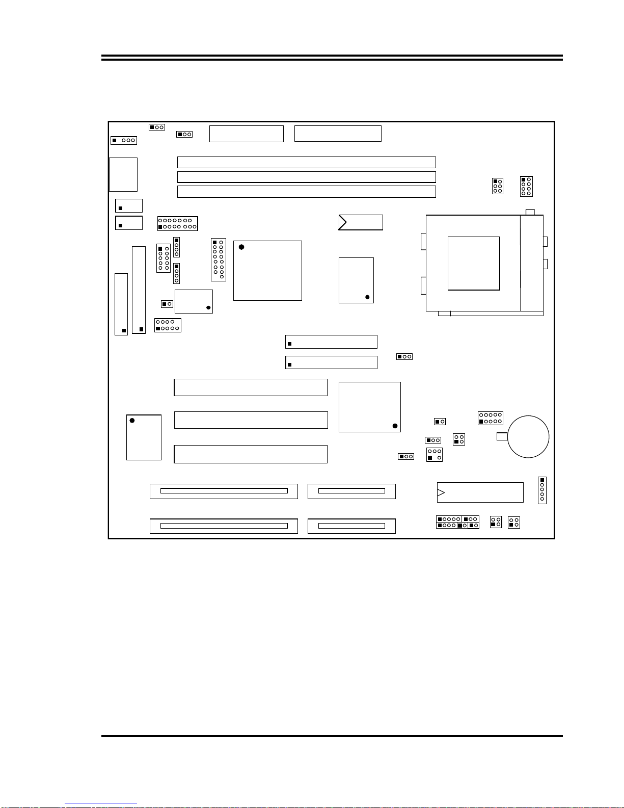
2-2 Mainboard Layout
J
2
K/B
CONN.
ZIF SOCKET 7
CPU
A
T POWER CONN.
PW2
FDD1
2
1
IDE1
2
1
IDE2
2
1
39
40
39
40
LPT1
U4
530
PW1
ATX POWER CONN.
COM
2
COM1
64KX64
SL
2
SL1
USB1
2
110
9
BATT.
+
J1
1
PCI 2
PCI
3
PCI 1
WOL
13
BIO
S
JP6
S
Y
S
FAN1
13
ITE8661
F
U18
J5
2
1
2 4
JP9
1 3
KEYLOCK TBS
W
SPEAKER RST TBLED
PS-ON
JP13
JP4
CPUFAN1
JP8
1
2
HDLED
SMI
ES1938S
JP1
13
AUDI
O
U24
DIMM2
DIMM1
DIMM3
GAM
E
VGA1
IR1
1
U16
5595
32K
X
8
1
JP3 JP2
1
JP11
1
JP1
2
1
Figure 2-1
2-3 Quick Reference for Jumpers, Connectors &
5
Expansion Socket
Jumpers
Jumper Name Description Page
JP6 CMOS RAM Clear 2-3 Normal ,1-2 Clear CMOS p. 8
JP8 CPU Voltage selector for detail page 7 p. 6
JP2,JP3 Jumpers for CPU type selection for detail page 7 p. 6
Connectors
Connector Name Description Page
J2 Keyboard Connector 5-Pin Female p.10
USB1 USB Port Connector 10-Pin Block p.13
J1 PS/2 Mouse Connector 6-Pin Block p.10
COM1,COM2 Serial Port COMA & COMB 10-Pin Block p.11
LPT1 Parallel Port Connector 26-Pin Block p.11
FDD1 Floppy Driver Connector 34-Pin Block p.11
IDE1 Primary IDE Connector 40-Pin Block p.11
IDE2 Secondary IDE Connector 40-Pin Block p.12
VGA1 VGA Connector 16-Pin Block p.14
CPUFAN1
SYSFAN1 FAN Connector 1-2 12V Power Connector
2-3 ACPI FAN power control
Connector
p.13
IR1 Infrared Module Connector 5-Pin Block p.13
PW2 AT Power Connector 12-Pin Block p. 9
PW1 ATX Power Connector 20-Pin Block p.410
HDLED IDE activity LED 2-Pin Connector p.12
FPC Front Panel Connector 16-Pin Block p.12
PS-ON ATX power button/soft power button 2-Pin connector p.13
Audio Audio connector 10-pin connector p.14
Game Game port connector 16-pin connector p.14
JP12 CD-Audio/Panasonic 4-pin Block p.14
JP11 CD-Audio/Sony/IDE 4-pin Block p.14
WOL Wake On Lan 3-pin Block p.15
JP13 Audio chip Enabled/Disabled On-Enabled , Off-Disabled p.15
J5 SB_Link connector 6-pin connector p.15
JP1 Keyboard Voltage selector 1-2 : 5VSB , 2-3 : Vcc p.15
Expansion Sockets
Socket/Slot Name Description Page
SL1, SL2 ISA Slot 16-bits ISA Bus Expansion slots p.9
PCI1, PCI2, PCI3 PCI Slot 32-bits PCI Local Bus Expansion slots p.9
DIMM1,DIMM2,
DIMM3 DIMM Module Socket 168-Pins DIMM SDRAM Module
Expansion Socket p.8
ZIF SOCKET 7 CPU Socket Pentium CPU Socket p.9
2-4 Installation Steps

6
Before using your computer, you must follow the steps as follows:
1. Set Jumpers on the Motherboard
2. Install the CPU
3. Install DRAM Modules
4. Install Expansion card
5. Connect Cables, Wires, and Power Supply
2-5 Jumper Settings
1. CPU Voltage Selection: JP8 (2x5pin Block)
This jumper is used for adjusting CPU working voltage, for this main board design it
can auto detect the single voltage CPU or dual voltage CPU.
The table of JP8 CPU voltage selection {S : short (ON) , O : open (OFF)}
JP8 1-2 3-4 5-6 7-8 9-10
1.8V O S O S S
2.0V O S S S S
2.1V S O O O O
2.2V O S O O O
2.3V S S O O O
2.4V O O S O O
2.5V S O S O O
2.8V O O O S O
2.9V S O O S O
3.1V S S O S O
3.2V O O S S O
3.3V S O S S O
3.5V S S S S O
If your CPU Type is not including in above table, please refer to the CPU voltage selection
on below to choose the correct working voltage for your CPU.
CPU Volta
g
e Selection
1.8V
JP8
1
2
9
10
2.0V
JP8
1
2
9
10
2.8V
JP8
1
2
9
10
2.9V
JP8
1
2
9
10
3.1V
JP8
1
2
9
10
3.2V
JP8
1
2
9
10
3.3V
JP8
1
2
9
10
3.5V
JP8
1
2
9
10
2.2V
JP8
1
2
9
10
2.5V
JP8
1
2
9
10
2.4V
JP8
1
2
9
10
2.3V
JP8
1
2
9
10
2.1V
JP8
1
2
9
10
2. CPU Type selection: JP2 &JP3
This mainboard designs JP2 to select the CPU, external clock (Host Bus Frequency)
and JP3 to select the CPU Bus Frequency ratio, the external clock frequency
multiplied by Bus frequency ratio is the CPU frequency as the tables below:
Table for CPU external frequency / SDRAM Clock setting : JP2
SD FS2 FS1 FS0 CPU Bus Clock SDRAM Clock
7
O S S S 66.8 MHz 66.8 MHz
O S S O 75 MHz 75 MHz
O S O S 83.3 MHz 83 MHz
O S O O 95 MHz 95 MHz
O O S S 100 MHz 100 MHz
O O S O 112 MHz 112 MHz
S S S S 90/66.8 MHz 90/89 MHz *
S S S O 83.3 MHz 66.8 MHz *
S S O S 95 MHz 63.3 MHz *
S S O O 100 MHz 66.6 MHz *
S O S S 100/105 MHz 75 MHz *
S O S O 112 MHz 74.4 MHz *
※ SDRAM Clock Asynchronous as CPU Bus frequency let user can use slow
speed SDRAM when CPU clock over 83MHz.{ S : short (ON) O : open (OFF) }
For ICS9248-81 clock Generator
Table for CPU ratio selector : JP3
CPU ratio BF0 BF1 BF2
1.5 X / 3.5 X OFF OFF OFF
2.0 X ON OFF OFF
2.5 X ON ON OFF
3.0 X OFF ON OFF
4.0 X ON OFF ON
4.5 X ON ON ON
5.0 X OFF ON ON
5.5 x OFF OFF ON
Table for CPU Type selection :
JP2 (Bus clock) JP3 (clock ratio)
CPU Type SD FS2 FS1 FS0 BF0 BF1 BF2
Bus clock Clock ratio
233MHz Pentium processor
with MMX technology
AMD K6-233
Cyrix 6X86 MII 300
O S S S O O O 66MHz 3.5X
200MHz Pentium processor
with MMX technology
AMD K6-200
Cyrix/IBM 6X86 MII 233
O S S S O S O 66MHz 3.0X
AMD K6/266, K6-2/266 O S S S S O S 66MHz 4.0X
AMD K6/300 O S S S S S S 66MHz 4.5X
AMD K6-2/300 O O S S O S O 100MHz 3.0X
AMD K6-2/333 O S O O O O O 95MHz 3.5X
AMD K6-2/350 O O S S O O O 100MHz 3.5X
AMD K6-2/400, K6-3/400 O O S S S O S 100MHz 4.0X
AMD K6-2/450, K6-3/450 O O S S S S S 100MHz 4.5X
AMD K6-2/500, K6-3/500 O O S S O S S 100MHz 5.0X
AMD K6-2/550, K6-3/550 O O S S O O S 100MHz 5.5X
Cyrix MII-266 O S O S S S O 83MHz 2.5X
Cyrix MII-333 O S O S O S O 83MHz 3.0X
Cyrix MII-333 O S S O O O O 75MHz 3.5X
Cyrix MII-366 O O S S S S O 100MHz 2.5X
Cyrix MII-400 O S O O O S O 95MHz 3.0X
Cyrix MII-433 O O S S O S O 100MHz 3.0X
IDT Winchip-225 O S S O O S O 75MHz 3.0X

8
NOTE:
c
Before installing the CPU, Please check the CPU Frequency and Clock Ratio from
your supplier.
d
For Cyrix/IBM 6X86MX series, please double check the CPU’s Frequency and
Clock Ratio.
JP3
1
JP2
1
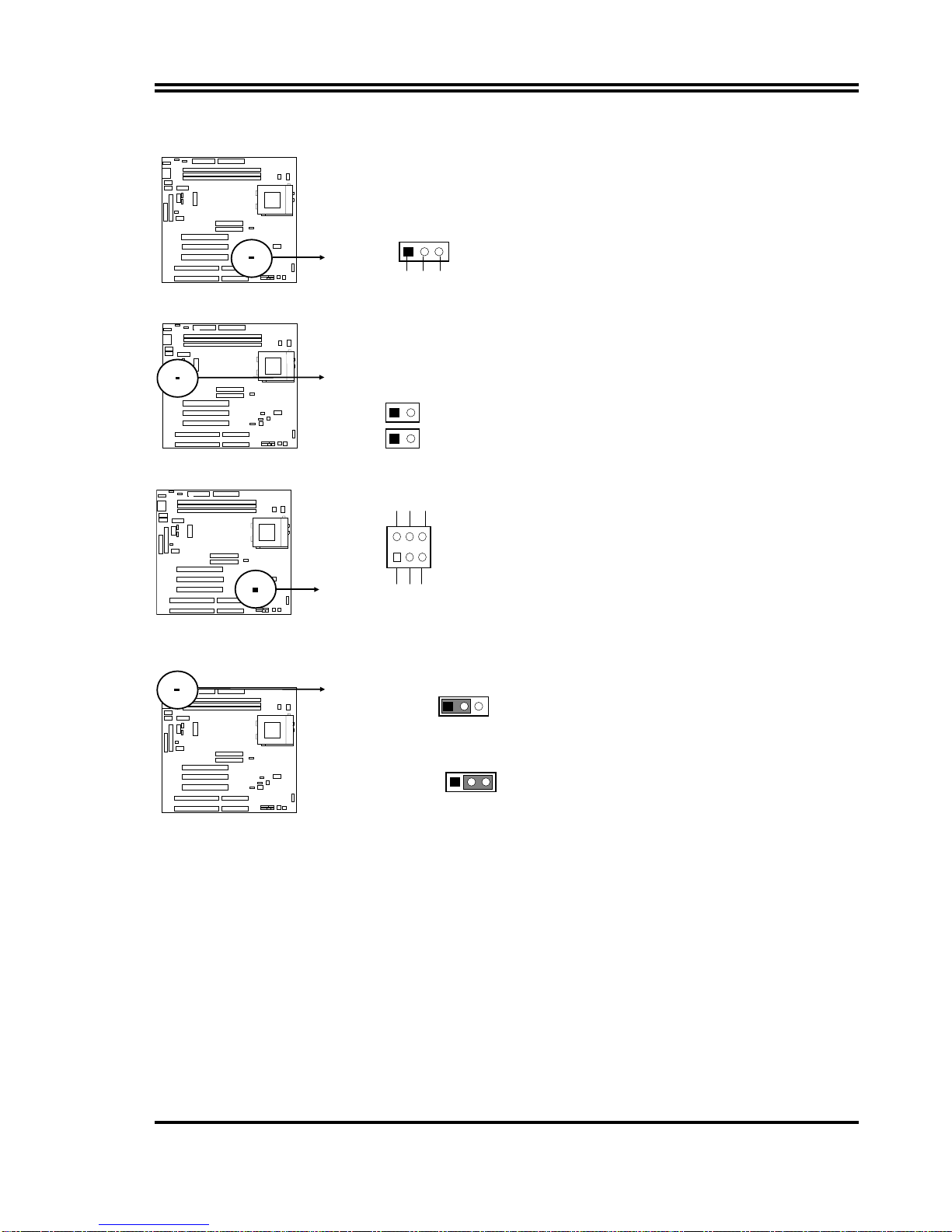
3. CMOS RAM Clear: JP6 (Yellow color selector)
WARNING: Make sure your computer is POWER OFF when you CLEAR CMOS.
Connect a jumper Cap over this jumper for a few seconds, will clears information
stored in the CMOS RAM Chip that input by user, such as hard disk information and
passwords. After CLEAR CMOS, you must enter the BIOS setup (by holding down
<DEL> during power-up) to re-enter BIOS information (see BIOS SETUP).
Selections JP6
Normal 2-3 (Default)
Clear CMOS 1-2 (momentarily)
Normal
CMOS RAM (Normal / Clear CMOS Data)
JP6
123
Clear CMOS
JP6
123
2-6 System Memory (DRAM)
This main board supports three 168-pins DIMM modules, the Max Memory Size is 768MB
Because of the VGA share memory function, the system must always occupy BANK0
(DIMM1)to booting.
DIMM 1 DIMM 2 DIMM 3 System can be
Accept or Not
168-pin DIMM Accept
168-pin DIMM 168-pin DIMM Accept
168-pin DIMM 168-Pin DIMM Accept
168-pin DIMM 168-pin DIMM 168-pin DIMM Accept
168-pin DIMM Not Accept
168-pin DIMM Not Accept
168-pin DIMM 168-pin DIMM Not Accept
The SDRAM clock can choice Synchronous(# SD open) or Asynchronous(# SD
closed) by the jumper setting of JP2, let user more choice of SDRAM .
9
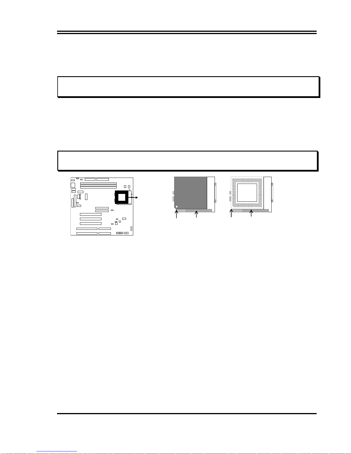
2-7 Central Processing Unit (CPU)
The main board provides a 321-pins ZIF Socket 7. The CPU on mother board must have
a fan attached to prevent overheating.
WARNING: Without a fan, the CPU will be overheated and cause damage to both the CPU
and the motherboard.
To install a CPU, first turn off your system and remove its cover. Locate the ZIF socket
and open it by first pulling the lever sideways away from the socket then upwards to a 90-
degree right angle. Insert the CPU with the white dot as your guide. The white dot should
point towards the end of the level. The CPU has a corner pin for three of the four corners,
the CPU will only fit in the one orientation as shown as follow. With the added weight of
the CPU fan, no force is required to insert the CPU. Once completely inserted, hold down
on the fan and close the socket’s lever.
IMPORTANT: You must set jumpers JP2,JP3 “CPU Type selector” on page 5 and jumper JP8 “CPU
Voltage Selection” on page 5 depending on the CPU that you install.
CPU ZIF Socket 7
Lock
Socket 7
Blank
Socket 7
Lever
White Dot
CPU
2-8 Expansion Cards
First read your expansion card documentation on any hardware and software settings that
may be required to setup your specific card.
Installation Procedure:
1. Read the documentation for your expansion card.
2. Set any necessary jumpers on your expansion card.
3. Remove your computer’s cover.
4. Remove the bracket on the slot you intend to use.
5. Carefully align the card’s connectors and press firmly.
6. Secure the card on the slot with the screw you remove in step 4.
7. Replace the computer’s cover.
8. Setup the BIOS if necessary.
9. Install the necessary software drivers for your expansion card.
2-9 External Connectors
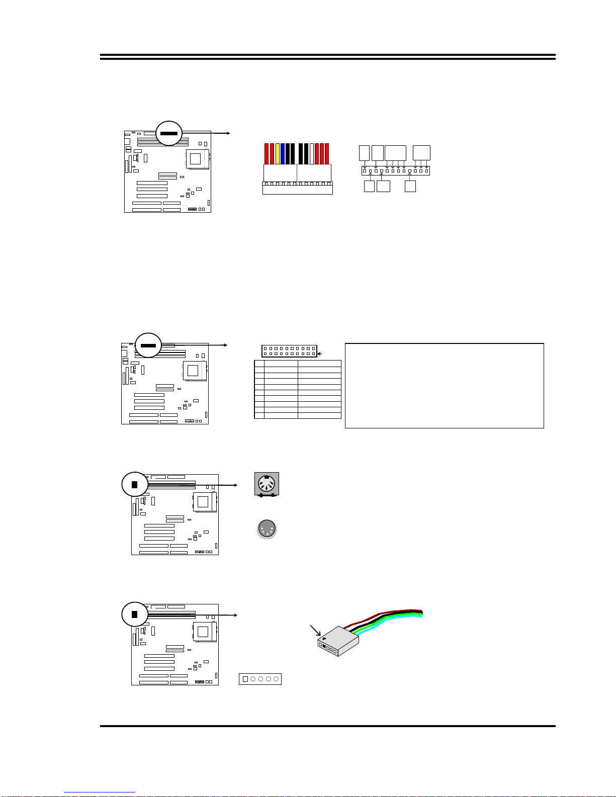
1. Power connector: AT Power Connector (12-pin block): PW2
This connector connects to a standard AT power supply. To connect the leads from
the power supply, ensure first that the power supply is not plugged. Most power
supplies provide two plugs (P8 and P9), each containing six wires, two of which are
black. Orient the connectors so that the black wires are located in the middle.
10
Using a slight angle, align the plastic guide pins on the lead to their receptacles on the
connector. Once aligned, press the lead onto the connector until the lead locks into
place.
Power Plugs from Power Supply
Power Connector on Motherboard
PG +12V GND
+5V -12V -5V
+5V
P8 P9
O
R
R
E
Y
L
B
L
B
L
B
L
B
L
B
L
W
H
R
E
R
E
R
E
2. Power Connector: ATX Power Connector (20-pin block): PW1
ATX Power Supply connector. This is a new defined 20-pins connector that usually
comes with ATX case. The ATX Power Supply allows to use soft power on
momentary switch that connect from the front panel switch to 2-pins Power On jumper
pole on the motherboard. When the power switch on the back of the ATX power
supply turned on, the full power will not come into the system board until the front
panel switch is momentarily pressed. Press this switch again will turn off the power to
the system board.
PIN ROW2 ROW1
1 3.3V 3.3V
2 -12V 3.3V
3 GND GND
4 Soft Power On 5V
5 GND GND
6 GND 5V
7 GND GND
8 -5V Power OK
9 +5V +5V
(
for Soft Lo
g
ic
)
Pin 1
3. Keyboard Connector (5-pin female): J2
This connection is for a standard IBM-compatible keyboard. May also be known as a
101 enhanced keyboard.
Keyboard Connector (5-pins female)
Connector Plug from Keyboard
4. PS/2 Mouse Connector (6-pin block): J1
If you are using a PS/2 mouse, you must purchase an optional PS/2 mouse set which
connects to the 6-pins block and mounts to an open slot on your computer‘s case.
1: DATA
2: NC
3: GND
4: VCC
5: CLK
PIN 1
PS/2 Mouse Module Connector
* Please don’t turn off / on power
supply two quickly ,we recommend
aleast wait 4sec before turn on the
power , to protect the system

11
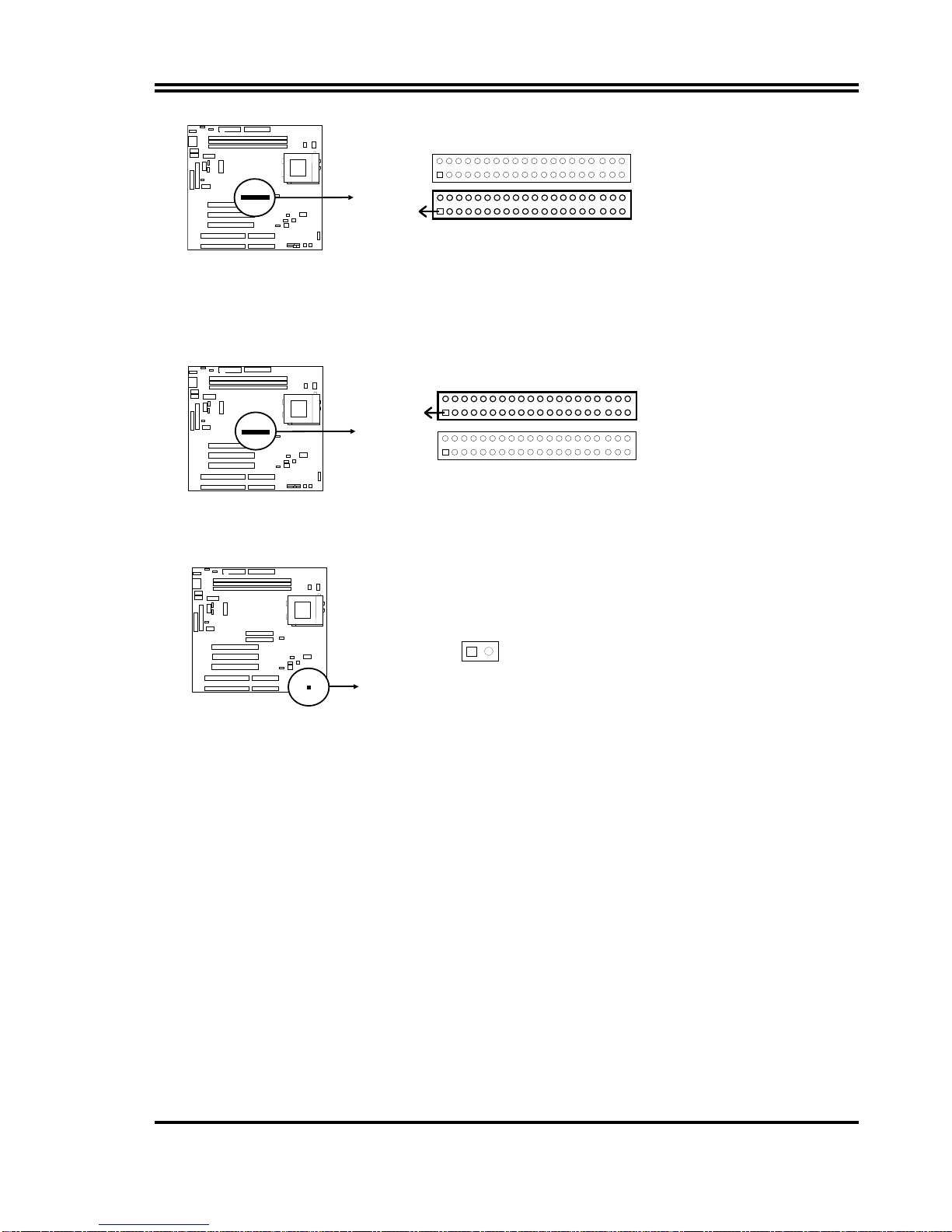
5. Parallel Printer Connector (26-pin Block): LPT1
Connection for the enclosed parallel port ribbon cable with mounting bracket. Connect
the ribbon cable to this connection and mount the bracket to the case on an open slot.
It will then be available for a parallel printer cable.
NOTE: Serial printers must be connected to the serial port. You can enable the parallel port and choose
the IRQ through BIOS Setup.
Pin 1
Parallel Printer Connector
LPT1
6. Serial port COMA and COMB Connector (Two 10-pin blocks): COM1, COM2
These connectors support the provided serial port ribbon cables with mounting bracket.
Connect the ribbon cables to these connectors and mount the bracket to the case on
an open slot. The two serial ports on the mounting bracket will then be used for
pointing devices or other serial devices. See BIOS configuration of “Onboard Serial
Port”
COM 1
Pin 1
Pin 1
COM 2
Serial port COMA and COMB Connector
7. Floppy drive Connector (34-pin block): FDD1
This connector supports the provided floppy drive ribbon cable. After connecting the
single plug end to motherboard, connect the two plugs at other end to the floppy
drives.
Pin 1
Flo
ppy
Drive Connector
FDD1
8. Primary IDE Connector (40-pin block): IDE1
This connector supports the provided IDE hard disk ribbon cable. After connecting the
single plug end to motherboard, connect the two plugs at other end to your hard
disk(s). If you install two hard disks, you must configure the second drive to Slave
mode by setting its jumpers accordingly. Please refer to the documentation of your
hard disk for the jumper settings.
12
Primary IDE Connector
Pin 1
9. Secondary IDE Connector (40-pin block): IDE2
This connector connects to the next set of Master and Slave hard disks. Follow the
same procedure described for the primary IDE connector. You may also configure
two hard disks to be both Masters using one ribbon cable on the primary IDE
connector and another ribbon cable on the secondary IDE connector.
Secondary IDE Connector
Pin 1
10. IDE activity LED: HDLED
This connector connects to the hard disk activity indicator light on the case.
HDLED
IDE (Hard Drive) LED
-+
31
11. Front Panel connector: This 16-pin connector to connect to case front panel switch.
A. Turbo LED switch: TBLED
The motherboard‘s turbo function is always on. The turbo LED will remain
constantly lit while the system power is on. You may also to connect the Power
LED from the system case to this lead. See the figure below.
B. Reset switch lead: RST
This 2-pin connector connects to the case-mounted reset switch for rebooting your
computer without having to turn off your power switch. This is a preferred method
of rebooting in order to prolong the life of the system‘s power supply. See the
figure below.
C. Keyboard lock switch lead & Power LED: KEYLOCK & PW
This 5-pin connector connects to the case-mounted key switch for locking the
keyboard for security purposes and Power LED together.
D. Speaker connector: SPEAKER
This 4-pin connector connects to the case-mounted speaker. See the figure below.
13
System Case Connections
GND
Turbo
LED
Reset
SW
V
CC
GND
Speaker
VCC GND
NC
GND NC
GND
VCC
GND
Power LED/
ACPI LED
Turbo SW/
SMI
Keyboard
Lock
12. IR infrared module connector: IR1
This connector supports the optional wireless transmitting and receiving infrared
module. This module mounts to small opening on system cases that support this
feature you must also configure the setting through BIOS setup. Use the five pins as
shown on the Back View and connect a ribbon cable from the module to the
motherboard according to the pin definitions.
Infrared Module Connector
IR1
N.C
IRRX
GND
IRTX
V
CC 1
2
3
4
5
13. USB Port connector: USB1
Pin 1
USB1
USB Port Connector
Vcc
V
c
c
+DAT
A
NC
-DATA
GND
-DATA
NC
GND
+ DATA
14. FAN connector: CPUFAN1 , SYSFAN1
SYSFAN1
1
CPU Fan Connector
1CPUFAN1
15. ATX Power button/ Soft Power button: PS-ON
When using ATX power, the system power can be controlled by a momentary switch
connected to PS-ON Pushing the button once will switch the system between ON and
SLEEP. Pushing the switch while in the ON mode more than 4 seconds will turn the
system off. The system Power LED shows the status of the system’s power.
Selections PS-ON
One touch Power ON/OFF 2-4
14
ATX Power button/Soft Power button
PS-ON
1
3
24
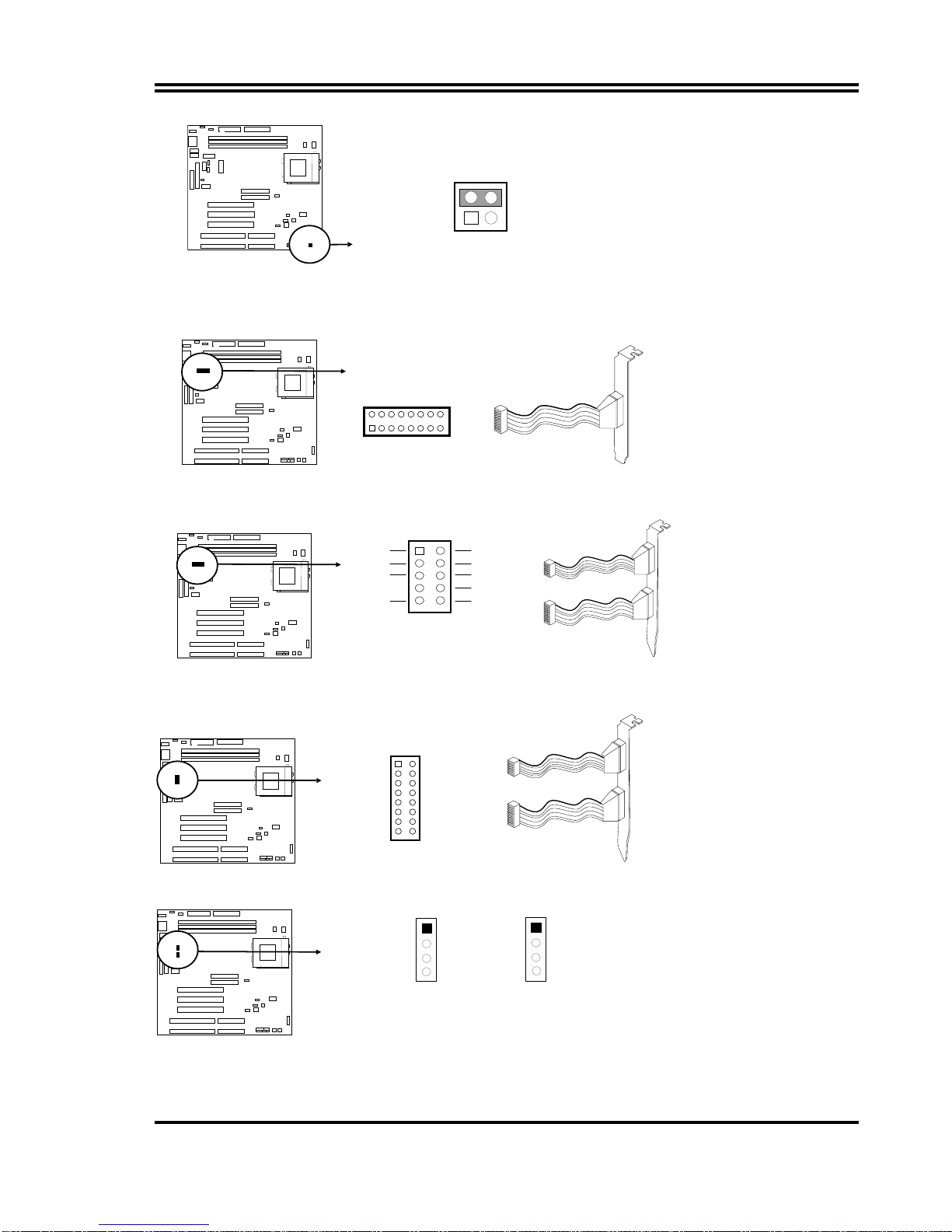
16. VGA connector: VGA1
This connector supports the provided VGA cable with mounting bracket. Connect the
ribbon cable to connector and mount the bracket to the case on an open slot .
VGA Connector
1
V
GA1
215
16
Orient the red stripe on the
monitor cable with Pin 1
17. Audio connector: Audio
Audio Connector
JP21 12
910
GN
D
MICP
L – I N - R
GN
D
L – OUT - R
GND
MIC
L – OUT -
L
L – I N - L
Orient the red stripe on the
monitor cable with Pin 1
Audio
Game
18. Game Port connector: GAME
GAME PORT Connector
GAM
E
12
15 16
Orient the red stripe on the
monitor cable with Pin 1
Audio
Game
19. CD-ROM Audio connector: JP11,JP12
Panasonic
CD-ROM Audio connector
JP11
Sony
JP121
2
3
4
1
2
3
4
15
20. Wake On Lan connector: WOL
WON
1
+5VSB GND WON
21. On Board Audio chip Enbled / Disabled connector: JP13
JP1
3
1Closed (Default) : Enabled
Open (Default) : Disabled
22. SB_Link connector: J5
Audio Connector
J5
1
2
PCREQ* SI RQGND
NC GNDPCGNT*
23.Keyboard Voltage: JP1
JP1
1
1-2 closed for 5VSB in Keyboard power
ON Function when use ATX power
JP1
1
2-3 closed for Vcc

16
Chapter 3
AWARD BIOS SETUP
Award's ROM BIOS provides a built-in Setup program which allows user modify the basic
system configuration and hardware parameters. The modified data will be stored in a
battery-backed CMOS RAM so data will be retained even when the power is turned off. In
general, the information saved in the CMOS RAM stay unchanged unless here is
configuration change in the system, such as hard drive replacement or new equipment is
installed.
It is possible that CMOS had a battery failure which cause data lose in CMOS_RAM. If so,
re_enter system configuration parameters become necessary.
To enter Setup Program
Power on the computer and press <Del> key immediately will bring you into BIOS CMOS
SETUP UTILITY.
ROM PCI/ISA BIOS (2A5IMJ1B)
CMOS SETUP UTILITY
AWARD SOFTWARE, INC.
STANDARD CMOS SETUP
BIOS FEATURES SETUP
CHIPSET FEATURES SETUP
POWER MANAGEMENT SETUP
PNP/PCI CONFIGURATION
LOAD BIOS DEFAULTS
LOAD SETUP DEFAULTS
INTEGRATED PERIPHERALS
SUPERVISOR PASSWORD
USER PASSWORD
IDE HDD AUTO DETECTION
SAVE & EXIT SETUP
EXIT WITHOUT SAVING
Esc : QUIT ↑↓→← : Select Item
F10 : Save & Exit Setup (Shift) F2 : Change Color
Figure 3-1
The menu displays all the major selection items and allow user to select any one of shown
item. The selection is made by moving cursor (press any direction key) to the item and
press <Enter> key. An on_line help message is displayed at the bottom of the screen as
cursor is moving to various items which provides user better understanding of each
function. When a selection is made, the menu of selected item will appear so the user
can modify associated configuration parameters.

17
3-1 STANDARD CMOS SETUP
Choose "STANDARD CMOS SETUP" in the CMOS SETUP UTILITY Menu (Figure 3-1).
The STANDARD CMOS SETUP allows user to configure system setting such as current
date and time, type of hard disk drive installed in the system, floppy drive type, and the
type of display monitor. Memory size is auto-detected by the BIOS and displayed for your
reference. When a field is highlighted (direction keys to move cursor and <Enter> key to
select), the entries in the field will be changed by pressing <PgDn> or <PgUp> keys or
user can enter new data directly from the keyboard.
ROM PCI/ISA BIOS (2A5IMJ1B)
STANDARD CMOS SETUP
AWARD SOFTWARE, INC.
Date (mm:dd:yy) : Thu, Mar, 12 1998
Time (hh:mm:ss) : 13 : 43 : 56
HARD DISKS TYPE SIZE CYLS HEAD PRECOMP LANDZ SECTOR MODE
Primary Master : Auto 0 0 0 0 0 0 Auto
Primary Slave : Auto 0 0 0 0 0 0 Auto
Secondary Master : Auto 0 0 0 0 0 0 Auto
Secondary Slave : Auto 0 0 0 0 0 0 Auto
Drive A : 1.44M , 3.5 in.
Drive B : None
Video : EGA/VGA
Halt On : All Errors
Base Memory : 640K
Extended Memory : 7168K
Other Memory : 384K
Total Memory : 8192K
Esc : Quit ↑↓→← : Select Item Pu/Pd/+/- : Modify
F1 : Help (Shift)F2: Change Color
Figure 3-2
NOTE: If hard disk Primary Master/Slave and Secondary Master/Slave were used Auto, than
the hard disk size and model will be auto-detect on display during POST.
NOTE: The "Halt On:" field is to determine when to halt the system by the BIOS is error
occurred during POST.

18
3-2 BIOS FEATURES SETUP
Select the "BIOS FEATURES SETUP" option in the CMOS SETUP UTILITY menu allows
user to change system related parameters in the displayed menu. This menu shows all of
the manufacturer's default values of this motherboard. Again, user can move the cursor by
pressing direction keys and <PgDn> of <PgUp> keys to modify the parameters. Pressing
[F1] key to display help message of the selected item.
This setup program also provide 2 convinent ways to load the default parameter data from
BIOS [F6] or CMOS [F7] area if shown data is corrupted. This provides the system a
capability to recover from any possible error.
ROM PCI/ISA BIOS (2A5IMJ1B)
BIOS FEATURES SETUP
AWARD SOFTWARE, INC.
Virus Warning : Disabled
CPU Internal Cache : Enabled
External Cache : Enabled
Quick Power On Self Test : Enabled
Boot Sequence : A,C,SCSI
Swap Floppy Drive : Disabled
Boot Up Floppy Seek : Enabled
Boot Up NumLock Status : On
Memory Pariy Check : Enabled
Typematic Rate Setting : Disabled
Typematic Rate (Chars/Sec) : 6
Typematic Delay (Msec) : 250
Security Option : Setup
Video BIOS Shadow : Enabled
C8000-CBFFF Shadow : Disabled
CC000-CFFFF Shadow : Disabled
D0000-D3FFF Shadow : Disabled
D4000-D7FFF Shadow : Disabled
D8000-DBFFF Shadow : Disabled
DC000-DFFFF Shadow : Disabled
PCI/VGA Palette Snoop : Disabled
OS Select For DRAM > 64MB : Non-OS2
Report No FDD For WIN 95 : No
Esc: Quit ↑↓→← : Select Item
F1 : Help Pu/Pd/+/-:Modify
F5 : Old Values (Shift)F2 : Color
F6 : Load BIOS Defaults
F7 : Load Setup Defaults
Figure 3-3
Note: The Security Option contains "setup" and "system". The "setup" indicates that the
password setting is for CMOS only while the "system" indicates the password setting is
for both CMOS and system boot up procedure.
Virus Warning: This category flashes on the screen. During and after the system
boots up, any attempt to write to the boot sector or partition table of the hard disk
drive will halt the system and the following error message will appear, in the mean
time, you can run an anti-virus program to locate the problem. Default value is
Disabled
Enabled:Activates automatically when the system boots up causing a warning
message to appear when anything attempts to access the boot sector or
hard disk partition table.
Table of contents
Other JETWAY Motherboard manuals

JETWAY
JETWAY 845GEFC User manual

JETWAY
JETWAY 866ASR2C Manual

JETWAY
JETWAY I407R1A User manual

JETWAY
JETWAY 939AGPECR110 User manual

JETWAY
JETWAY 694TCS User manual

JETWAY
JETWAY V4MDFTR1A User manual

JETWAY
JETWAY V500DAR1A User manual

JETWAY
JETWAY MI215 Series User manual

JETWAY
JETWAY J-630AF User manual

JETWAY
JETWAY JNF711-2807 User manual

JETWAY
JETWAY P4MVM User manual

JETWAY
JETWAY 915GCPR2A User manual

JETWAY
JETWAY BA-500PRO User manual

JETWAY
JETWAY 693AS User manual

JETWAY
JETWAY NC84 User manual

JETWAY
JETWAY 845GEA1A User manual

JETWAY
JETWAY 865PBAR1A User manual

JETWAY
JETWAY S445R1C User manual

JETWAY
JETWAY I402R2A User manual

JETWAY
JETWAY 618TAS3A User manual


