6
iCE40 Ultra Mobile Development Platform User Guide
Features
• Supports BLE (Bluetooth Low Energy) module
• Supports OTA (Over-The-Air) configuration of FPGA
• Form factor similar to mobile phone
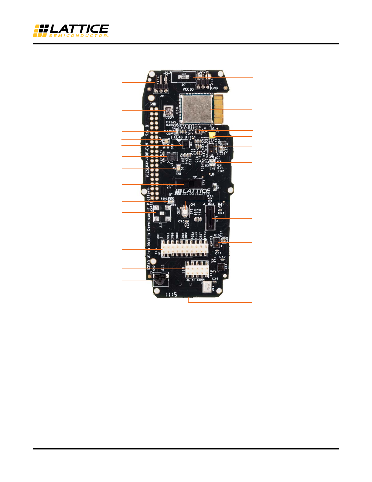
Sensor list
The following table lists the different sensors used on the board.
Table 1. Sensor List
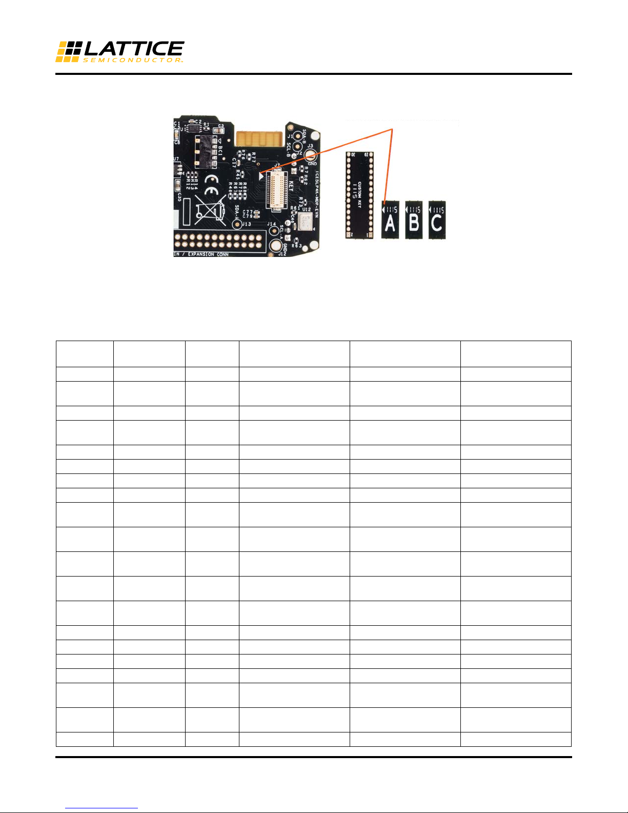
Key-socket Arrangement
Three predefined keys and one user defined key is provided to allow the user to change the wiring of the board
between different sensor sets as described in Table 2. The table also denotes pin assignments to the iCE40 Ultra
FPGA on the board. While selecting and inserting a particular key of choice, ensure that you align the aligning
arrow on the key and on the main PCB. The keys are mechanically delicate, and hence, you must be careful while
inserting and removing the keys. Figure 4 shows the four keys and socket on the main board.
Number Sensor Function Interface Sensor Part Number Manufacturer
1 RGB LED (Variant 1) Direct AEBMT-RGBZ AOT
2 RGB LED (Variant 2) Direct APTF1616SEEZGQBDC Kingbright
3 High Current IR Tx LED
(Variant A)
Direct SFH4645 Osram Opto
4 High Current IR Tx LED
(Variant B)
Direct VSMB2948SL Vishay Semiconductor
5 High Current Visible LED Direct XBDA WT-00-0000-
00000LCE3
Cree Inc.
6 IR Rx Direct TSMP58000 Vishay Semiconductor
7 Proximity Sensor
(Two numbers)
I2C TMD27711 A MS-TA OS USA Inc
8 RGB Light Sensor I2C MAX44008 Maxim-IC
9 Temperature Sensor I2C BMP180 (integrated) Bosch
10 Barometric Pressure I2C BMP180 Bosch
11 Accelerometer I2C LSM330DLC ST Micro
12 Gyroscope I2C
13 Magnetometer I2C LSM303DLHC ST Micro
14 Humidity I2C SHT20 Sensirion
15 Hall Direct BU52051NV X-TR Rohm Semiconductor
16 Fingerprint SPI FPC1080A Fingerprints
17 MEMS Mic (Two numbers) I2S ADMP441 Invensense